Suppressed conductance in a metallic graphene nano-junction
Abstract
The linear conductance spectrum of a metallic graphene junction formed by interconnecting two gapless graphene nanoribbons is calculated. A strong conductance suppression appears in the vicinity of the Dirac point. We found that such a conductance suppression arises from the antiresonance effect associated with the edge state localized at the zigzag-edged shoulder of the junction. The conductance valley due to the antiresonance is rather robust in the presence of the impurity and vacancy scattering. And the center of the conductance valley can be readily tuned by an electric field exerted on the wider nanoribbon.
pacs:
81.05.Uw, 73.40.Jn, 73.23.-b, 72.10.-dGraphene, an atomically thin layer of graphite, is regarded as a perspective base for the post-silicon electronics since its first experimental realization.refNovoselov1 Motivated by possible device applications, the electronic and transport properties of various graphene nano-structures have been studied both experimentally and theoretically, refD.A.Areshkin ; refB.Obradovic ; refM.Y.Han ; refY.Ouyang ; refA.Rycerz ; refT.B.Martins ; refhod ; refL.Brey ; refZ.p.Xu ; refS.Hong ; refT.C.Li Among these structures, graphene nanoribbon(GNR) is the basic element to carry the current. Band structure calculations indicate that the zigzag-edged graphene nanoribbons are always metallic while the armchair-edged ones are either metallic or semiconducting, depending on the width of the armchair GNR.refL.Brey A graphene junction can be formed by interconnecting two semi-infinite GNRs with different widths. In such a graphene nanostructure, a traveling carrier is scattered by the junction interface, which causes a finite junction conductance. Recently, the conductance spectrum of a graphene metal-semiconductor junctions has been studied in details.refT.C.Li ; refZ.p.Xu ; refS.Hong It has been found that the presence of the lattice vacancy can efficiently enhance the junction conductance, because that a vacancy makes the coupling between the electron states of the two GNRs at the junction interface stronger.
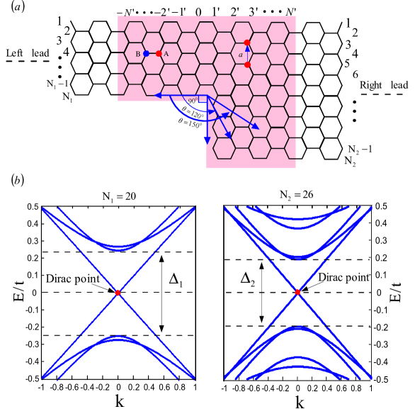
Apart from the metal-semiconductor junction, a metallic graphene junction can be constructed by interconnecting two metallic armchair GNRs with different widths. In this letter, we investigate the conductance spectrum of such a metallic graphene junction, the lattice structure of which is depicted in Fig.1(a). Unlike a metal-semiconductor junction,refZ.p.Xu ; refS.Hong the gapless subband structures of the two metallic armchair nanoribbons shown in Fig.1(b) indicates that electronic transmission through the metallic junction with an arbitrary energy is formally allowed. In particular, the electronic transmission via the linear subbands is reflectionless even in the presence of a long-range scattering potential, due to pseudospin conservation.refM.I.Katsnelson Therefore, a plausible anticipation is that the electronic transmission probability near the Dirac point should be close to unity. However, our calculation gives the opposite result: the junction conductance at the Dirac point is equal to zero, and a conductance valley appears around this point. This means a strong conductance suppression in the vicinity of the Dirac point. Further analysis demonstrates that the conductance suppression arises from the antiresonance due to the existence of an edge state localized in the shoulder region of the junction.
To calculate the linear conductance of the metallic graphene junction as a function of the incident electron energy , we adopt the Landauer-Bütikker formula in the discrete lattice representation.refF.M ; Datta It gives , where is a retarded Green function, and is the tight-binding Hamiltonian of the device region in the nearest-neighbor approximation. The contributions of the two semi-infinite leads are incorporated by the two self-energy terms which are associated with the coupling functions by . The two self-energy terms are obviously the key quantities for calculating the conductance, which can be evaluated by the recursive method.refF.M In what follows we use the lattice constant and the hopping energy between the nearest neighbor atoms as the units of the length and energy.
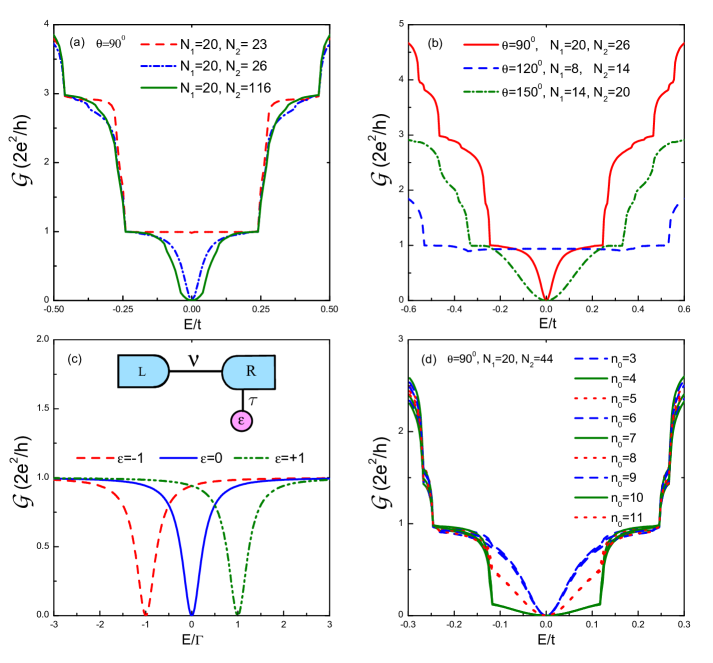
The calculated conductance spectra( vs ) for some typical square junctions() are shown in Fig.2(a). All these conductance spectra exhibit the staircase-like structures, which can be readily explained by matching of the subband structures of the two component ribbons as shown in Fig.1(b). Another point to note in Fig.2(a) is that the conductance spectrum shows a notable suppression in the vicinity of the Dirac point when the difference of the widths of the two GNRs is larger than 3. In particular, a zero conductance occurs at the Dirac point. However, from Fig.1(b) we can readily find that the linear subbands of the two ribbons always match each other to provide an electron transmission mode, and hence a nonzero conductance at the Dirac point, in contradiction with the calculated zero conductance. As shown in Fig.2(b), we find that the conductance suppression near the Dirac point is tightly associated with the zigzag edge of the shoulder of the junction. On the contrary, when the edge of shoulder is of an armchair type(), the conductance spectrum no longer shows any suppression. From such a result we infer that the nature of the conductance suppression is the antiresonance effect, the detail of which is as follows. In the vicinity of the Dirac point, only the linear subbands are relevant to the electron transmission. Hence the two metallic GNRs can be viewed as single mode quantum wires coupling to each other directly. However, the zigzag-edged shoulder induces a localized edge state with the eigen-energy equal to the Dirac energy. Such a localized state couples to the linear subband of the wider GNR. Consequently, when the electronic transport is limited to the vicinity of the Dirac point, the graphene junction is equivalent to the T-shaped quantum dot structure as shown in Fig.2(c). The linear conductance of such a model has been extensively studiedrefA. Ueda ; refY.Liu ; refW.J.Gong and can be expressed in terms of the model parameters
| (1) |
where and with being the electron density of the states in two leads. This expression presents a zero conductance at the quantum dot level , which is called the antiresonance effect. The antiresonance is in fact a result of quantum interference. The lateral quantum dot introduces new Feynman paths with a phase shift . As a result, the destructive quantum interference occurs among electron Feynman paths.refY.Liu ; refW.J.Gong In the metallic graphene junction, the edge state attached to the zigzag-edged shoulder of the junction plays a role of laterally coupled quantum dot, which results in the antiresonance at the Dirac point.
When the widths of the two GNRs are fixed, the geometry of the junction can be changed by shifting downwards the narrower ribbon. In Fig.2(d) the conductance spectra are compared for differently shaped junctions. We can see that the width of conductance valley depends on the junction shape sensitively. To be more specific, in terms of the valley width the spectra are classified into three groups, each of which appears periodically whenever the narrower ribbon shifts downwards by three multiples of the lattice constant. This phenomenon can be explained with the help of the above quantum dot model. The parameter in the quantum dot model is a relevant quantity to the width of the antiresonance valley. From Fig.1(a) we can see that is proportional to the product of the electron probability amplitudes of the A and B atoms interconnecting directly at the junction interface. And the probability amplitudes can be obtained by solving the Dirac equation refL.Brey . In such a way we work out the following relation , where is any odd number within the range from 1 to , and denotes the displacement of the narrower ribbon with respect to the upper edge of the wider ribbon. From this relation we can readily understand the periodic feature of the valley width of the conductance spectra shown in Fig.2(d).
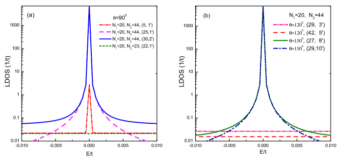
The antiresonance picture of the conductance suppression in the metallic graphene junction is further demonstrated by the calculated spectra of the local density of states (LDOS) at some lattice points near the junction interface. From Fig.3 we can see that only for the lattice points at the zigzag edge of the shoulder of junction( and ), the LDOS spectrum exhibits a very sharp peak at the Dirac point. This indicates the existence of a localized state in the shoulder region of the junction. An exception occurs for the junction with a very short shoulder( and in Fig.3(a)). The LDOS spectrum of the lattice point at the zigzag-edged shoulder does not show a notable peak. This result is consistent with the previous workrefhod , which argued that a zigzag edge of the width smaller than three lattice constant can not induce any localized edged state.
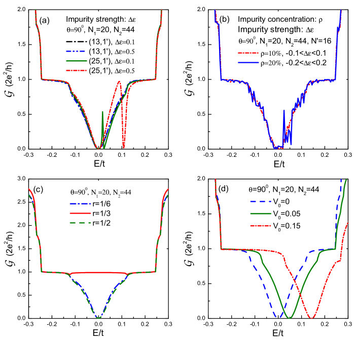
We now proceed on to discuss the influence of the possible scatterers in an actual graphene junction on the antiresonance valley. At first, we consider the individual effect of an impurity appearing at distinct positions. In the numerical calculation, an impurity is simulated by the deviation of the on-site energy of an specific lattice point where the impurity appears. The calculated conductance spectra with an individual impurity positioned at different lattice points are compared in Fig.4(a). We can see that only when the impurity appears in the shoulder region, the variation of the conductance spectrum is notable. But the effect of such an impurity is not to destroy the antiresonance at the Dirac point. Instead it causes another conductance zero near the Dirac point. This result implies that the edge state is intricately affected by an impurity in the shoulder region. On the contrary, the impurity at other lattice points can not modify the antiresonance valley notably since it is irrelevant to the edge state. Fig.4(b) shows the conductance spectrum in the presence of many impurities distributed randomly in the device region with fluctuating strengths. We can see that the antiresonance is rather robust even if the impurity concentration and strength are nontrivially large. Fig.4(c) shows the effect of vacancies positioned uniformly at the zigzag edge of the shoulder of a square junction. A vacancy is simulated in the numerical calculation by simply cutting off a carbon atom of type A at the edge of the shoulder. If we use the notations and to denote the atom number of type A belonging to the edge of the shoulder and the number of the vacancy in this edge respectively, the ratio can be viewed as the concentration of vacancy. From Fig.4(c) we can see only when the concentration of the vacancies is about , the zero conductance at the Dirac point can be completely eliminated. Higher or lower concentrations of vacancies can not destroy the conductance valley around the Dirac point. Our calculation also indicates that such a conclusion is independent of the size of the shoulder. This result implies the complicated effect of the edge defect on the edge state. Such an interesting topic is left for our study in the future. Finally, we can apply a step-like potential in the right hand side of the junction to tune the position of antiresonance, which can be simulated by shifting the on-site energy of all the lattice points of the wider GNR. The result is shown in Fig.4(d). We can see that the step-like potential simply shifts the antiresonance point, without drastically altering the lineshape of the conductance spectrum. What is noteworthy is that the conductance at the Dirac point can be easily tuned from zero to unity by a step-like potential. This suggests a possible device application of a nanoswitch based on such a metallic graphene junction.
This work was financially supported by the National Nature Science Foundation of China under Grant NNSFC10774055.
References
- (1) K. S. Novoselov, A. K. Geim, S. V. Morozov, D. Jiang, Y. Zhang, S. V. Dubonos, I. V. Grigorieva, and A. A. Firsov, Science 306, 666 (2004).
- (2) D. A. Areshkin and C. T. White, Nano Lett. 7, 3253 (2007).
- (3) B. Obradovic, R. Kotlyar, F. Heinz, P. Matagne, T. Rakshit, M. D. Giles, M. A. Stettler, and D. E. Nikonov, Appl. Phys. Lett. 88, 142102 (2006).
- (4) M. Y. Han, B. Özyilmaz, Y. Zhang, and P. Kim, Rev. Lett. 98, 206805 (2007).
- (5) Y. Ouyang, Y. Yoon, J. K. Fodor, and J. Guo, Appl. Phys. Lett. 89, 203107 (2006).
- (6) A. Rycerz, J. Tworzdlo, and C. W. J. Beenakker, Nat. Phys. 3, 172 (2007).
- (7) T. B. Martins, R. H. Miwa, A. J. R. da Silva, and A. Fazzio, Phys. Rev. Lett. 98, 196803 (2007).
- (8) L. Brey and H. A. Fertig, Phys. Rev. B 73, 235411 (2006).
- (9) O. Hod, V. Barone, and G. E. Scuseria, Phys. Rev. B 77, 035411 (2008).
- (10) T. C. Li and S. P. Lu, Phys. Rev. B 77, 085408 (2008).
- (11) Z. P. Xu and Q. S. Zheng, Appl. Phys. Lett. 90, 223115 (2007).
- (12) S. Hong, Y. Yoon, and J. Guo, Appl. Phys. Lett. 92, 083107 (2008).
- (13) M. I. Katsnelson, K. S. Novoselov, and A. K. Geim, Nat. Phys. 2, 620 (2006).
- (14) S. Datta, Electronic Transport in Mesoscopic Systems (Cambridge University Press, Cambridge, England, 1995).
- (15) F. Muñoz-Rojas, D. Jacob, J. Fernndez-Rossier, and J. J. Palacios, Phys. Rev. B 74, 195417 (2006).
- (16) A. Ueda and M. Eto, Phys. Rev. B 73, 235353 (2006).
- (17) Y. Liu, Y. Zheng, W. J. Gong, and T. Lü, Phys. Rev. B 75, 195316 (2007).
- (18) W. J. Gong, Y. Zheng, Y. Liu, and T. Lü, Physica E 40, 618 (2008).


