Resonant electronic states and - curves of Fe/MgO/Fe(100) tunnel junctions
Abstract
The bias dependence of the tunnel magnetoresistance (TMR) of Fe/MgO/Fe tunnel junctions is investigated theoretically with a fully self-consistent scheme that combines the non-equilibrium Green’s functions method with density functional theory. At voltages smaller than 20 mVolt the - characteristics and the TMR are dominated by resonant transport through narrow interface states in the minority spin-band. In the parallel configuration this contribution is quenched by a voltage comparable to the energy width of the interface state, whereas it persists at all voltages in the anti-parallel configuration. At higher bias the transport is mainly determined by the relative positions of the band-edges in the two Fe electrodes, which causes a decrease of the TMR.
pacs:
75.47.Jn,73.40.Gk,73.20.-rModern magnetic sensors, such as read heads for hard disk drives, are based on the tunnel magnetoresistance (TMR) effect. This is the drop in resistance of a magnetic tunnel junction (MTJ) formed by two magnetic layers when the mutual alignment of their magnetization vectors changes from antiparallel (AP) to parallel (P). The TMR magnitude is given by , with being the current at the voltage for the configuration (P or AP). Huge TMR ratios have been recently achieved in epitaxial, all crystalline Fe/MgO Yua2 and CoFeB/MgO Park1 MTJs, reaching up to 500% at room temperature and 1010% at 5 K Ohno1 . These large values of TMR are broadly attributed to the phase coherent and transverse momentum conserving transport. The TMR thus is governed not only by the spin-polarization of the electrode density of states (DOS), but also by the details of the wave-functions matching across the barrier. Magnetic transition metals with bcc crystal structure (Fe) possess a high transmission band, which decays slowly across the MgO barrier But1 . This is fractionally filled for majority spins (), and empty for minority spins (). Since these bands dominate the tunneling current, bcc transition metals with MgO barrier effectively behave as half-metals, and the TMR is expected to be very large But1 ; Math .
Another important, but much less investigated aspect, is the relation between electronic states and the - characteristics in these highly crystalline MTJs. Interfacial states and details of the Fe band-structure, otherwise washed out by disorder, play an important role in the transport and indeed can be identified through the - curves and its derivatives ( and ). For instance, high-quality conventional MTJs (2-3 nm MgO thickness) show a pronounced broad peak on the curve at about 1 Volt for the AP, and a number of small peaks at lower voltages in the P configuration Yua3 ; Tiusan:PRB08 . Combined with a quantitative theory these measurements can provide a wealth of information, and help on the level of device design. We note that very thin MTJs, with a MgO thickness of about 1 nm, have to be used for ultra high recording density (500 Gbit/inch2) HDD readers Yua1 . Remarkably, at these small MgO thicknesses, the growth mode of the Fe/MgO/Fe stack changes Tiusan:PRB08 .
In this letter we investigate theoretically the - characteristics of perfectly crystalline Fe/MgO MTJs, and demonstrate that its features originate from the sweeping of the band-edges and of interface states across the bias window. These generic features are emphasized here, as they resemble closely those studied in molecular devices NatMat and magnetic point contacts MPC . We investigate the ultra-thin MTJ regime, with the goal to provide a solid basis for decoding future - measurements of nm thick MgO barriers, in term of their relation to the underlying electronic structure and possibly growth defects. Calculations are performed using SMEAGOL Smeagol , which combines the non-equilibrium Green’s function method with density functional theory (DFT) Siesta . The total transmission coefficient is self-consistently evaluated at finite bias and integrated to give the spin-current.
| (1) |
Here is the spin index (, ) and is the Fermi function calculated at , with the Fe Fermi energy, the Boltzmann constant and the electronic temperature. Translational invariance allows to write where the integral runs over the 2D Brillouin zone perpendicular to the transport direction with area . Large -point samplings are necessary to converge , so that an extremely stable numerical algorithm is needed ivanselfenergy .
We consider a MTJ oriented along the Fe(100) direction and formed by 4 MgO monolayers (1.1 nm long). The atomic coordinates are those from reference bluegel1 , which have been optimized by high-accuracy plane-wave calculations. The unit cell used for the transport contains also 8 Fe atomic layers on each side of the MgO barrier, which are enough to screen the charge density from the interface. A 7x7 -points mesh converges the charge density, but a 100x100 mesh is used for evaluating . The basis set employed is single- for the Fe and orbitals, while double- is used for all other orbitals Siesta . The local density approximation (LDA) is adopted throughout, and we use a real space mesh cutoff of 600 Ry and K.
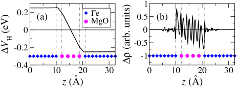
First, we look at the electrostatic Hartree potential drop across the junction. In Fig. 1(a) we show the difference between the planar average of the self-consistent Hartree potential at a finite bias and that at 0-bias along the junction stack (-axis). is flat in the electrodes and decays linearly in the MgO, demonstrating that the usual approximation of shifting rigidly the electronic structure of the electrodes and then applying a linear potential drop across the barrier Mertig is well justified. In Fig. 1(b) we also show the difference between the planar average of the self-consistent charge density at a finite bias and at 0-bias, so that . At all voltages we find increasing linearly with , and charge accumulating at the extremal layers of the electrodes just before MgO. Inside the MgO oscillates due to the electric field induced polarization. This is confirmed by a DFT calculation for an isolated MgO slab of the same thickness in an equivalent electric field, which shows analogous oscillations.
We start our analysis of the transport properties by presenting (Fig. 2).
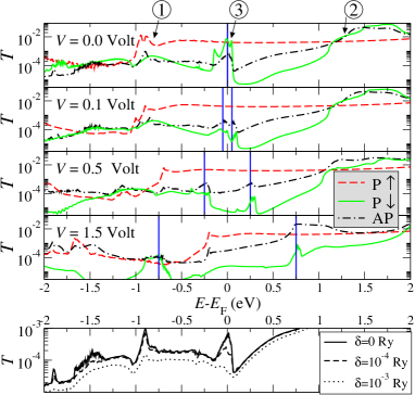
Three main features appear in the transmission coefficient: ➀ a sharp increase (note the logarithmic scale) in transmission at around -1 eV for the spins in the P configuration, ➁ a similar, although smoother increase above +1 eV for the spin in the P configuration and for the AP configuration, and ➂ a sharp resonance at for the spins in the P configuration, which is still visible in the AP configuration.
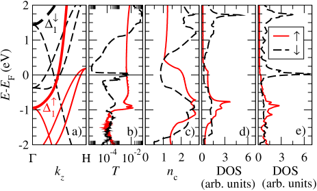
The first two features are associated with the band-edges, respectively for the and spins, as it can be clearly seen in Fig. 3. Note also that these band-edges coincide with energy regions where the average number of Fe-channels per -point is maximized [Fig. 3(c)]. Since these
are a feature of the electronic structure of Fe alone, their position as a function of bias is set by the quasi Fermi energies, , of the two electrodes. For instance the sharp increase of in the P configuration (➀) moves to -0.75 eV and -0.25 eV respectively for voltages of 0.5 Volt and 1.5 Volt, following the band-edge of the left lead. In the same way the broad peak in both P and AP at about 1.5 eV above (➁) splits into two broad sub-peaks, separated by . Note however that whereas the height of the peak is roughly constant for the AP configuration, in the P configuration the sub-peak entering the bias window shrinks drastically.
In contrast the peak in transmission at for the spins in the P configuration and in the AP configuration cannot be associated with leads band-edges but instead originates from a narrow interface state in the minority band IvanJEMS ; But1 ; Tsym1 . This is spatially localized at the interface between Fe and MgO and it is resonating at . A comparison between the bulk Fe DOS and the DOS for the interface Fe layer [Figs. 3(d) and (e)] indicates the surface state for spins at But1 . The dynamics of such a interface state under bias can be understood from the cartoon of figure 4.
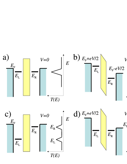
Consider the panels (a) and (b) where two identical interface states are localized on either sides of the tunnel barrier. This is the situation encountered here for the spins. The transport is then resonating across the barrier at the interface state energy . In the case considered here the resonance energy is close to .
Since, in general the state is coupled more strongly to one of the electrodes, it will trace closely its quasi Fermi energy. For instance for positive bias and a interface state localized on the left-hand (right-hand) side of the junction [Fig. 4(b)] we obtain (). This brings the states on either side of the junction out of resonance and generally suppresses the transmission. Thus the peak in , originating from a resonating interface state across the barrier, will evolve into two smaller peaks separated by an energy . Indeed this is the behavior observed in Fig. 2. For instance the two peaks centered at are separated by 0.5 eV and 1.5 eV respectively for voltages of 0.5 Volt and 1.5 Volt. In the AP configuration this situation is found at any bias, since the spin interface state is always present on one side of the junction only.
A second possible situation is when the interface states on the left-hand and right-hand side of the tunnel junction have a different origin and are placed at different energy. In this case we do not expect zero-bias resonance, however there will be a critical voltage at which the resonant condition is met. In this case we expect the rise of a large peak in the transmission coefficient at a bias . This situation has never been encountered for the symmetric MTJ investigated here, but it is likely to be the most typical case in real junctions.
We now move to analyzing the - characteristic and the TMR (Fig. 5), starting from the
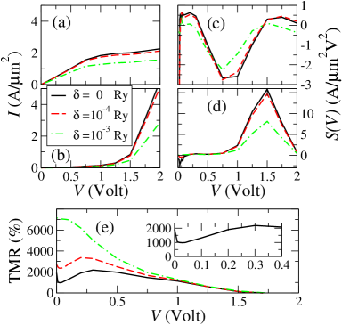
low bias region ( 0.4 Volt). The most apparent feature in this bias range is a sharp reduction of the TMR from its zero-bias value followed by a rapid increase which peaks at Volt. The sharp reduction can be associated with a decrease in the P current originating from the loss of the interface state resonant condition at mVolt, a bias which roughly corresponds to the line-width of the interface state. For 20 mVolt the P current is shared by the two spin-species, while for 20 mVolt the component dominates. Such a reduction in the P component at the bias corresponding to the resonant condition loss can be clearly observed in the plot of Fig. 5(c). As the bias further increases the conductance in the P configuration is approximately constant. In contrast the conductance of the AP configuration is reduced for between 0.1 and 0.3 Volt, and this behavior results in an increase of the TMR with the broad peak at 0.3 Volt.
The high bias region is characterized by a decrease of the conductance in the P configuration at around 1 Volt and a dramatic increase of the AP current for Volt. This produces a strong reduction of the TMR with bias and an almost complete suppression for Volt. In fact at about 1.75 Volt the TMR becomes negative. Such a voltage range should be put in comparison with the band offset. In our LDA calculations for Fe is positioned 1.8 eV below the MgO conduction band minimum and 3.0 eV above the valence band maximum. This means that voltages of the order of 1.5 Volt are still rather far from those needed for tunneling across a reduced barrier.
The high-bias behavior is dominated by the relative energy shift with bias of the Fe states. The origin of the reduction of the conductance in the P configuration for 1 Volt is that once the band-edge of the left lead enters the bias window, the high transmission region only extends over part of such window (Fig. 2), so that the increase of the current with bias is reduced by a factor of about 2. Note that the current in the is negligible. The broad peak of the transmission at about 1.5 eV above the Fermi energy, related to the band-edge, never contributes significantly to the current in the P configuration. The reason is that whereas for positive bias the band-edge of the right lead enters the bias window, the one on the left lead moves away from the bias window, so that the peak shrinks as bias is applied. The general evolution with bias of this transmission peak resembles the one of the surface states schematically shown in Figs. 4(a) and (b). In the AP configuration however this peak does contribute to the current, since electrons belonging to the band in the right lead that are inside the bias window can tunnel into the bands of the left lead. This leads to an increase of the conductance once the band-edge moves into the bias window, resulting in a drastic increase of the AP current at Volt. We note that our results in the high bias region are in contrast with those in reference guo2 , in which a rapid increase of the conductance is found also for the P configuration.
It is also interesting to comment on the plots [Fig.5(c) and (d)]. For both the magnetic configurations one can observe a peaked structure. This is observed also experimentally Yua3 and attributed to resonances in the transmission. At the qualitative level this interpretation is confirmed by our results in the low bias region, where the interface states determine the behavior of the -. The actual position of the peaks however depends on the atomic details of the two interfaces and we do not expect agreement. The high-bias region however is more problematic. In particular we note that our - for the P configuration does not increase as rapidly as that found in typical experiments. One possible explanation for such difference is that the MgO barrier calculated here is very thin and the current consequently already large at small bias, another reason could be presence of defects at the interface and in the MgO in experiments.
Finally we investigate the effect of generic disorder, motivated by observations Tiusan:PRB08 . This is modeled at a simple level by adding a small imaginary part to the energy when calculating , i.e. it corresponds to a uniform level broadening Tsym1 . The effects of such addition on the -, and TMR are shown in Fig. 5, while those on for the AP configuration are shown in Fig. 2. Fig. 2 clearly shows that increasing results in a gradual suppression of the resonance at . For Ry the peak is still clearly visible, and only for Ry it completely disappears. As a result the TMR at low bias largely increases and the non-monotonic behavior for Volt is suppressed. In contrast the high bias region is barely affected by . These results, although indicative of the effects of disorder on the TMR, should be taken with caution. The broadening introduces unstructured disorder, and the transmission of all the spin-channels is equally reduced. In reality one may expect the transmission to either increase or decrease depending on the type of scattering center, which in general will act differently on the different spin-channels. This will in general result in an enhancement of the current in the AP alignment, causing a reduction of the TMR.
In conclusion, we investigated the bias dependence of the TMR of an epitaxial Fe/MgO/Fe tunnel junction. We identify two different bias regions, which are affected by two types of electronic resonances: (i) interface resonance states and (ii) band edges. The low bias region is characterized by a non-monotonic behavior of the TMR caused by resonant scattering across the barrier due to the highly localized interface states. In the high bias region ( Volt) the TMR decreases monotonically, mainly due to band edge states. We have also shown how disorder can suppress the transport through interface states and smoothens the TMR.
This work is sponsored by Science Foundation of Ireland ( 07/IN.1/I945 and 07/RFP/PHYF235) and by Seagate. Computational resources have been provided by TCHPC and ICHEC. O.M. acknowledges the SFI C.T.Walton fellowship support during his stay at Trinity College.
References
- (1) S. Yuasa, T. Nagahama, A. Fukushima, Y. Suzuki and K. Ando, Nature Mater. 3, 868 (2004).
- (2) S.S.P. Parkin et al., Nature Mater. 3, 862 (2004).
- (3) Y.M. Lee, J. Hayakawa, S. Ikeda, F. Matsukura and H. Ohno, Appl. Phys. Lett. 90, 212507 (2007).
- (4) W.H. Butler, X.-G. Zhang, T.C. Schulthess and J.M. MacLaren, Phys. Rev. B 63, 054416 (2001).
- (5) J. Mathon and A. Umerski, Phys. Rev. B 63, 220403(R) (2001).
- (6) Y. Ando et al., Appl. Phys. Lett. 87, 142502 (2005).
- (7) P. J. Zermatten et al., Phys. Rev. B 78, 033301 (2008) and references therein.
- (8) S. Yuasa and D.D. Djayaprawira, J. Phys. D: Appl. Phys. 40, R337 (2007).
- (9) A.R. Rocha et al., Nature Materials 4, 335 (2005).
- (10) A.R. Rocha and S. Sanvito, Phys. Rev. B 70 094406 (2004).
- (11) A.R. Rocha et al., Phys. Rev. B 73, 085414 (2006).
- (12) J.M. Soler et al., J. Phys.: Condens. Matter 14, 2745 (2002).
- (13) I. Rungger and S. Sanvito, Phys. Rev. B, 78, 035407 (2008).
- (14) D. Wortmann, G. Bihlmayer and S. Blügel, J. Phys.: Condens. Matter 16, S5819 (2004).
- (15) C. Heiliger, P. Zahn, B. Yu. Yavorsky and I. Mertig, Phys. Rev. B bf 73, 214441 (2006).
- (16) I. Rungger, A.R. Rocha, O. Mryasov, O. Heinonen and S. Sanvito, J. Magn. Magn. Mater. 316, 481 (2007).
- (17) K. D. Belashchenko, J. Velev and E. Y. Tsymbal, Phys. Rev. B 72, 140404(R) (2005).
- (18) D. Waldron, L. Liu and H. Guo, Nanotechnology 18, 424026 (2007).