Atomic Hole Doping of Graphene
Graphene is an excellent candidate for the next generation of electronic materials due to the strict two-dimensionality of its electronic structure as well as the extremely high carrier mobility Novoselov ; de Heer ; Geim . A prerequisite for the development of graphene based electronics is the reliable control of the type and density of the charge carriers by external (gate) and internal (doping) means. While gating has been successfully demonstrated for graphene flakes Novoselov ; Oostinga ; Zhang and epitaxial graphene on silicon carbide Kedzierski ; Gu , the development of reliable chemical doping methods turns out to be a real challenge. In particular hole doping is an unsolved issue. So far it has only been achieved with reactive molecular adsorbates, which are largely incompatible with any device technology. Here we show by angle-resolved photoemission spectroscopy that atomic doping of an epitaxial graphene layer on a silicon carbide substrate with bismuth, antimony or gold presents effective means of p-type doping. Not only is the atomic doping the method of choice for the internal control of the carrier density. In combination with the intrinsic n-type character of epitaxial graphene on SiC, the charge carriers can be tuned from electrons to holes, without affecting the conical band structure.
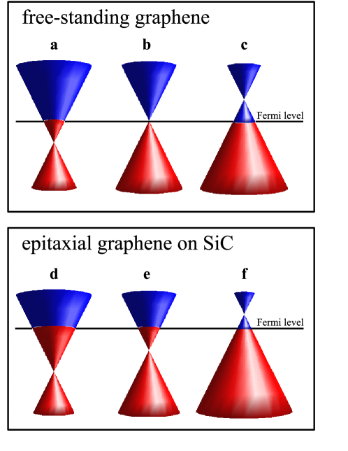
The recent interest in graphene — single layers of graphite — is based on its peculiar electronic structure. Two-dimensional by nature, it is a zero-gap semiconductor, i. e. a semimetal, with a conically shaped valence and conduction band reminiscent of relativistic Dirac cones for massless particles Wallace ; Slonczewski . As this kind of band structure provides great potential for electronic devices, one of the key questions is how to dope the electronic structure with electrons or holes appropriately for the different devices (see Fig. 1). The semimetallic character induced by the close proximity of valence and conduction band as well as the conical shape of the bands result from a delicate balance between the electrons and the lattice. The challenge here is to interact with the system just enough to add or remove electrons but not too much so as to modify or even collapse the electronic structure. Therefore, it is not an option to replace atoms within the graphene layer, as is common practice when doping silicon.

For graphene the doping is usually realized by adsorbing atoms and/or molecules on its surface, i. e. surface transfer doping Maier ; Chakrapani ; Ristein ; Sque . For n-type (p-type) doping the electrons have to be easily released into (extracted out of) the graphene layer. As alkali atoms easily release their valence electron, they very effectively induce n-type doping Bostwick ; Ohta (see Fig. 1(d)). The Dirac point, where the apices of the two conically shaped bands meet, is shifted further into the occupied states away from the Fermi level. However, aside from the fact that epitaxial graphene on silicon carbide is naturally n-doped, alkali atoms are very reactive and their suitability in electronic devices is more than questionable.
P-type doping for graphene is quite a bit more challenging. Many of the elements with a high electronegativity — e. g. nitrogen, oxygen, or fluorine — form strong dimer bonds. They would not likely form a stable adlayer on the graphene surface. Therefore, different molecules such as NO2, H2O, NH3, or the charge transfer complex tetrafluoro-tetracyanoquinodimethane (F4-TCNQ) have been used to induce p-type doping in graphene (see Fig. 1(f)) Chen ; Hwang ; Wehling ; Zhou3 . However, NO2, H2O and NH3 are very reactive chemicals and therefore not suitable for use in an electronic material. F4-TCNQ on the other hand plays an important role in optimizing the performance in organic light emitting diodes Blochwitz ; Zhou2 , but would also be difficult to implement in large scale fabrication. A viable alternative is presented by the heavier elements, which are not as reactive as, e. g. oxygen or fluorine. Although not obvious, because their electron affinity is somewhat lower than that of atomic carbon, bismuth as well as antimony turn out to be able to extract electrons out of the graphene sheet.

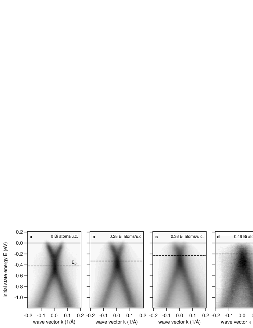
We have studied the valence band structure of a single graphene layer on 4H-SiC(0001) using angle-resolved photoemission spectroscopy. Fig. 2 shows the experimental band structure of epitaxial graphene doped with successively higher amounts of Bi atoms. The initial state energy of the bands is plotted as a function of the electron wave vector GK . The intensity scale is linear with light and dark areas corresponding to low and high photoelectron current, respectively. The Dirac point is located at the -point, which lies in the corner of the hexagonal Brillouin zone. Fig. 2(a) shows the pristine graphene layer. The linear dispersion of the valence and conduction bands is clearly visible. Due to the charge transfer with the SiC-substrate, the Dirac cone of the conduction band is partially filled shifting the Dirac point into the occupied states by about 420 meV Bostwick ; Zhou ; Riedl . In Figs. 2 (b)–(d) successively higher amounts of bismuth atoms per graphene unit cell (u.c.) as indicated in each panel are deposited on the graphene layer graphene . As the bismuth coverage increases the Dirac point clearly shifts towards the Fermi level. Otherwise, the band structure remains unaltered by the bismuth adatoms, i. e. the linear dispersion is preserved. Only at high bismuth coverage the line width of the bands increases noticeably. This is probably related to the Bi atoms not forming an ordered structure on the surface, which leads to broadening of the photoemission features. Furthermore, the number of free charge carriers decreases as a successively smaller cross section of the conduction band intersects the Fermi level.
Very similar results have been obtained for antimony atoms deposited on the graphene layer. Antimony is also located in group V of the periodic table just above bismuth, so that a very similar doping behavior is expected. The experimental band structure is not shown here, but looks very much like the data obtained for bismuth on graphene except that it takes a higher antimony coverage to reach the same doping level.

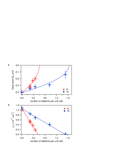
A more quantitative analysis of the bismuth and antimony doping is displayed in Fig. 3. Panel (a) shows the evolution of the Dirac point as a function of the coverage, which is given in number of atoms per graphene unit cell. The Dirac point clearly approaches the Fermi level with increasing doping indicating that there is charge transfer from the graphene layer to the adatoms. A simple theoretical model based on the linear density of states for the graphene layer has been used to estimate the doping effect of the bismuth atoms assuming that the charge transfer is proportional to the amount of dopant atoms:
| (1) |
Here is the Dirac point, with the zero of the energy scale referenced to the Fermi level. The Fermi velocity is eVÅ Geim ; Bostwick , is the number of electrons in the conduction band for zero doping, and is the number of holes doped into the graphene layer. If we assume that about 0.01 electrons per bismuth atom and 0.0036 electrons per antimony atom are extracted from the graphene layer, the Dirac point should follow the respective solid lines plotted in Fig. 3(a). It would reach the Fermi level for a coverage of 0.61 bismuth atoms and 1.65 antimony atoms per unit cell. The experiment shows, however, that for higher coverages the bands become broader and less well-defined. At these points the average distance between adatoms approaches the one of monolayer coverage, so that the photoelectrons will interact and scatter in the adlayer.

In Fig. 3(b), the free charge carrier density of the graphene layer is plotted as a function of adatoms per unit cell. It has been extracted from the experimental data through the Fermi wave vector via , a formula which relates Fermi wave vector and free charge carrier density for two-dimensional electron gases. The charge carrier density is clearly reduced as the number of adatoms increases indicating hole doping. The solid line shows a linear dependence of the charge carrier density as a function of bismuth coverage with a very good correspondence to the experimental data assuming the same values for the electron transfer per adatom as above.
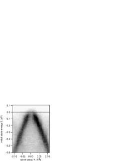
For actual p-type doping with holes as charge carriers, the Dirac point has to shift into the unoccupied states. A further increase of the electron transfer from the graphene layer to the adatoms is desirable. The natural starting point would be an element with a higher electron affinity than bismuth or antimony. Motivated by this, we have deposited gold atoms on epitaxial graphene, as its electron affinity is about twice as high as for bismuth and as recent phototransport experiments indicated that gold contacts induce p-doping in graphene Lee . The experimental band structure for about two gold atoms per graphene unit cell shown in (Fig. 4) clearly displays p-type doping. Both branches of the valence band cone clearly cross the Fermi level close to the -point leaving the valence band partially unoccupied. We estimate the Dirac point to be about 100 meV above the Fermi level and a free charge carrier density of the holes of about cm-2.
The bands in Fig. 4 are much narrower than for the bismuth adatoms in Fig. 2(d) even though the gold coverage is much higher than the bismuth coverage. The sharp bandstructure suggests that gold forms an ordered structure on the graphene layer. Furthermore, the p-type doping in Fig. 4 is only induced after a post-annealing of the sample to at least 700∘C. Similar to what has been observed for gold atoms binding to pentacene Repp , an actual bond between the gold atom and the graphene is formed after a certain activation barrier is overcome. The chemical bond formation is confirmed by x-ray photoelectron spectroscopy results, showing a clear splitting of the carbon 1s core level after annealing the sample at 700∘C, which is not present for the clean graphene layer. Interestingly, while this goes beyond the idea of surface transfer doping, where a covalent bond between adatom and graphene layer is not present, the peculiar band structure of graphene with its linear dispersion remains intact. This clearly demonstrates that for a coverage of about two gold atoms per graphene unit cell the Dirac point can be shifted above the Fermi level leaving the valence band partially unoccupied. Surprisingly, the estimated electron transfer is only 0.0024 electrons per gold atom, which is only a quarter of the value found for bismuth, where, however, no chemical bond to the graphene layer is formed.
Our results demonstrate that p-type doping of an epitaxial graphene layer is possible by means of simple atoms. While bismuth and antimony were only able to shift the Dirac point in the direction of the Fermi level, i. e. reduce the natural n-type doping of the substrate, gold actually shifted the Dirac point into the unoccupied states thereby inducing p-type doping. Epitaxial graphene on silicon carbide becomes a feasible alternative to conventional electronic materials as n-type doping is naturally induced and p-type doping can be achieved by doping with gold atoms, which are easily processed. With its potential for large scale production Kedzierski all the advantages of epitaxial graphene, e. g. the strict two-dimensionality, high carrier mobility, high current densities and ballistic transport at room temperature Geim , are available for device application.
Methods
Photoemission experiments have been done in ultra-high-vacuum (UHV). The UHV system is equipped with a hemispherical SPECS HSA3500 electron analyser with an energy resolution of 10meV. We used HeII radiation with an energy of 40.8eV for the ARUPS measurements. Our n-doped 4H-SiC(0001) substrate was prepared by hydrogen-etching and subsequent Si deposition at 800∘C until a homogeneous and sharp () LEED pattern appeared. A monolayer graphene was obtained after annealing for 5min at 1150∘C. Bi and Sb were deposited on a room temperature sample using a commercial electron beam evaporator which was calibrated with the help of the () reconstruction that is formed for 1/3 monolayer coverage of both Bi and Sb on Ag(111). Au was deposited at room temperature with a commercial Knudsen cell which was calibrated using a quartz crystal microbalance. After Au deposition the sample was annealed at 700∘C for 5min. All measurements were conducted at room temperature.
References
- (1) Novoselov, K. S., Geim, A. K., Morozov, S. V., Jiang, D., Zhang, Y. et al. Electric Field Effect in Atomically Thin Carbon Films. Science 306, 666 (2004)
- (2) de Heer, W.A., Berger, C., Wu, X., First, P. N., Conrad, E. H. et al. Epitaxial graphene. Solid State Commun. 143, 92 (2007)
- (3) Geim, A. K. & Novoselov, K. S. The rise of graphene. Nature Mater. 6, 183 (2007)
- (4) Oostinga, J. B., Heersche, H. B., Liu, X., Morpurgo, A. F. & Vandersypen, L. M. K. Gate-induced insulating state in bilayer graphene devices. Nature Mater. 7, 151 (2008)
- (5) Zhang, Y., Tan, Y.-W., Stormer, H. L. & Kim, P. Experimental observation of the quantum Hall effect and Berry’s phase in graphene. Nature 438, 201 (2005)
- (6) Kedzierski, J., Hsu, P.-L., Healey, P., Wyatt, P. W., Keast, C. L. et al. Epitaxial Graphene Transistors on SiC Substrates. IEEE Trans. Electron Devices 55, 2078 (2008)
- (7) Gu, G., Nie, S., Feenstra, W. J., Devaty, R. P., Choyke, W. J. et al. Field effect in epitaxial graphene on a silicon carbide substrate. Appl. Phys. Lett. 90, 253507 (2007)
- (8) Wallace, P. R. The Band Theory of Graphite. Phys. Rev. 71, 622 (1947)
- (9) Slonczewski, J. C. & Weiss, P. R. Band Structure of Graphite. Phys. Rev. 109, 272 (1958)
- (10) Maier, F., Riedel, B., Mantel, J. & Ristein, J. Origin of Surface Conductivity in Diamond. Phys. Rev. Lett. 85, 3472 (2000)
- (11) Chakrapani, V., Angus, J. C., Anderson, A. B., Wolter, S. D., Stoner, B. R. et al. Charge Transfer Equilibria Between Diamond and an Aqueous Oxygen Electrochemical Redox Couple. Science 318, 1424 (2007)
- (12) Ristein, J. Surface Transfer Doping of Semiconductors. Science 313, 1057 (2006)
- (13) Sque, S. J., Jones, R. & Briddon, P. R. The transfer doping of graphite and graphene. Phys. Stat. Sol. (a) 204, 3078 (2007)
- (14) Bostwick, A., Ohta, T., Seyller, T., Horn, K. & Rotenberg, E. Quasiparticle dynamics in graphene. Nature Phys 3, 36 (2007)
- (15) Ohta, T., Bostwick, A., Seyller, T., Horn, K. & Rotenberg, E. Controlling the Electronic Structure of Bilayer Graphene. Science 313, 951 (2006)
- (16) Chen, W., Chen, S., Qui, D. C., Gao, X. Y. & Wee, A. T. S. Surface Transfer p-Type Doping of Epitaxial Graphene. J. Am. Chem. Soc. 129, 10419 (2007)
- (17) Hwang, E. H., Adam, S. & Das Sarma, S. Transport in chemically doped graphene in the presence of adsorbed molecules. Phys. Rev. B 76, 195421 (2007)
- (18) Wehling, T. O., Novoselov, K. S., Morozov, S. V., Vdovin, E. E., Katsnelson, M. I. et al. Molecular Doping of Graphene. Nano Lett. 8, 173 (2008)
- (19) Zhou, S. Y., Siegel, D. A., Fedorov, A. V. & Lanzara, A. Metal to insulator transition in epitaxial graphene induced by molecular doping. arXiv:cond-mat:0807.4791 (2008)
- (20) Blochwitz, J., Pfeiffer, M., Fritz, T. & Leo, K. Low voltage organic light emitting diodes featuring doped phthalocyanine as hole transport material. Appl. Phys. Lett. 73, 729 (1998)
- (21) Zhou, X., Pfeiffer, M., Blochwitz, J., Werner, A., Nollau, A. et al. Very-low-operating-voltage organic light-emitting diodes using a p-doped amorphous hole injection layer. Appl. Phys. Lett. 78, 410 (2001)
- (22) The measurements were taken at the -point with the wave vector axis perpendicular to the -high symmetry line.
- (23) Zhou, S. Y., Gweon, G.-H., Fedorov, A. V., First, P. N., de Heer, W. A. et al. Substrate-induced bandgap opening in epitaxial graphene. Nature Mater. 6, 770 (2007)
- (24) Riedl, C., Zakharov, A. A. & Starke, U. Precise in situ thickness analysis of epitaxial graphene layers on SiC(0001) using low-energy electron diffraction and angle resolved ultraviolet photoelectron spectroscopy. Appl. Phys. Lett. 93, 033106 (2008)
- (25) The graphene unit cell used here has a lattice constant of 2.46 Å (hexagonal lattice) and contains two graphene atoms.
- (26) Lee, E. J. H., Balasubramanian, K., Weitz, R. T., Burghard, M. & Kern, K. Contact and edge effects in graphene devices. doi:10.1038/nnano.2008.172 (2008)
- (27) Repp, J., Meyer, G., Paavilainen, S., Olsson, F. E. & Persson, M. Imaging Bond Formation Between a Gold Atom and Pentacene on an Insulating Surface. Science 312, 1196 (2006)