Kondo effect in single atom contacts: the importance of the atomic geometry
Abstract
Co single atom junctions on copper surfaces are studied by scanning tunneling microscopy and ab-initio calculations. The Kondo temperature of single cobalt atoms on the Cu(111) surface has been measured at various tip-sample distances ranging from tunneling to the point contact regime. The experiments show a constant Kondo temperature for a whole range of tip-substrate distances consistently with the predicted energy position of the spin-polarized d-levels of Co. This is in striking difference to experiments on Co/Cu(100) junctions, where a substantial increase of the Kondo temperature has been found. Our calculations reveal that the different behavior of the Co adatoms on the two Cu surfaces originates from the interplay between the structural relaxations and the electronic properties in the near-contact regime.
pacs:
68.37.Ef, 73.20.Hb, 73.63.Rt,71.15.Ap 75.75.+aThe electron transport properties in a circuit, whose dimensions are reduced to single atom/molecule contact, is dominated by the quantum character of matter cuniberti05 and requires a deep understanding of its nanometer scale properties. Additionally, the electron transport through such a junction is strongly influenced by the coupling of the orbitals of the electrodes to the bridging molecule or atom tao08 . Accessing the correct information of the geometrical arrangement of the contact is fundamental to the interpretation of the experimental data. This is often challenging, despite the continuous progress in understanding the electron transport through nanometer scale junctions scheer98 ; yanson98 ; pascual95 ; lortscher07 ; burgi99 ; neel07 ; termirov08 ; xiao04 . Among other techniques such as mechanical controlled break-junction scheer98 ; yanson98 ; lortscher07 or electro-migration park99 , a junction achieved with the tip of a scanning tunneling microscope (STM) on a metal surface gimzewski95 ; burgi99 ; neel07 ; termirov08 has been proven as a valuable tool to target and select the substrate configuration before and after the contact is formed. Nonetheless, a general picture on the influence of atomistic order on the electron conductance at nanometer scale junctions is, at present, still missing.
Co adatoms on copper surfaces constitute an ideal system for studying the electron transport through nanometer scale junctions. The interplay of the unpaired electrons of single Co atoms and the free electron states on copper surfaces leads to the formation of a narrow electronic resonance at the Fermi level known as the Kondo resonance. This has been extensively characterized in tunneling conditions madhavan98 ; wahl04 ; knorr02 . One main result of these studies is the evidence that on different supporting surfaces the width of this resonance coincides with a change of the occupation of the d electron levels of the Co adatom wahl04 . This inherently reflects a varied coupling of the magnetic impurity to the metal substrate. Indeed, a simple model has been suggested to relate the energy position of the electron d-levels of the impurity and the atomic arrangement in close proximity of the Co adatom wahl04 ; knorr02 . Specifically, a narrower Kondo resonance is observed for Co adatoms on Cu(111) than on the Cu(100) surface in agreement with a shift in energy of the d-levels i.e with an increase in their occupation from the first to the second surface knorr02 ; wahl04 . Due to this dependence, the width of the Kondo resonance is then a good reference parameter to characterize the influence of the tip at reduced distances. However, it is a priori not evident if the width of the Kondo resonance will follow a trend similar to the one observed in tunneling configuration on various surfaces also when the tip is approached to the point contact configuration.
In order to address this question we measured the current-voltage characteristics at different tip-sample distances ranging from tunneling to point contact on individual Co adatoms on a Cu(111) surface. As will be shown in the following, the width of the Kondo resonance is practically constant on this surface at all tip-substrate distances in an apparent contradiction with the previously reported results on Cu(100) neel07 .
Based on ab-initio theoretical calculations aimed to determine the electronic and magnetic properties of these two systems, we will show that the opposing results observed on the two copper surfaces are not contradicting but demonstrate nicely the determining influence of the local atomic structure on the transport properties of a nanoscale junction.
The experiments were performed using a home built scanning tunneling microscope operated at 6K in ultra high vacuum (UHV) with a base pressure of 1*10-11mbar. The Cu(111) single crystal has been cleaned in UHV by cycles of Ar ion sputtering and annealing. Co single atoms have been deposited from a thoroughly degassed Co wire wound around a tungsten filament on the Cu surface at 20K. This resulted in a coverage of about 10-3ML of isolated immobile Co adatoms. The STM tip, chemically etched from tungsten wire, was treated in vacuo by electron field emission and soft indentation into the copper surface. This assured a spectroscopically featureless tip near the Fermi energy. Given this preparation, the tip was most likely covered by copper atoms deriving from the substrate.
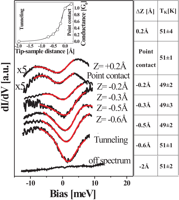
The inset in figure 1 shows the conductance of a single Co adatom at various tip-substrate displacements. This has been achieved by recording the current while approaching the tip towards the atom, in open feedback loop conditions. As the tip substrate distance is reduced the current increases smoothly from the tunneling to the point contact regime following the exponential dependence with the tip-substrate distance (z) characteristic of the electron tunneling process I(z)=I0exp(-Az) (where A is proportional to the work function of tip and substrate). Fitting the experimental curve, we obtained a work function for the Co/Cu(111) system of 5 eV. As the point contact regime is reached the current is found to exhibit a characteristic quantization plateau with only a weak dependence on the distance. The plateau is observed to be 1G0 where G0 is the conductance quantum G0=2e2/h (h is Planck constant) in agreement with studies on Co/Cu(100)neel07 . Topographic images acquired before and after the tip was approached and retracted from the point contact configuration confirm that the contact region as well as the tip have not changed during the tip displacements.

Information on the Kondo resonance have been obtained recording the dI/dV spectra on top of the Co adatom at various tip-substrate displacements. In figure 1, we report the spectra obtained at the tip-substrate separation indicated by the circles in the inset. The current versus voltage is measured with a lock-in amplifier applying a voltage modulation in the range of 1 to 0.1mV (rms). All the curves obtained in the range from the initial tunneling (Z=-2Å) to the point contact (Z=0.2Å) condition show a characteristic dip in the local density of states at an energy close to the Fermi level. This dip, which is due to the Kondo resonance can be characterized according to its width E, which is proportional to the Kondo temperature TK, E=2kBTK, where kB is the Boltzmann constant madhavan98 ; wahl04 . The Kondo Temperature can be extracted from these curves by fitting the experimental spectra with a Fano line function according to dI/dV(q+)2/(1+), with =(eV-K)/kBTK where q and define the asymmetry of the curve and the energy position of the resonance with respect to the Fermi energy fano61 . The fitted Kondo temperature TK is reported in figure 1 for each sampled tip position. As can be seen, the Kondo temperature for the Co on Cu(111) system is constant, within the experimental error, from the tunneling to the point contact regime.
The observed behavior of the Kondo temperature on the Cu(111) surface contrasts with the behavior previously reported for the Co/Cu(100) system, where a considerable increase of the Kondo temperature (from 70-90K in tunneling to 150K in point contact) was observed neel07 . As will be shown below this difference can be ascribed to the sensitivity of the Kondo effect to the local atomic geometry.
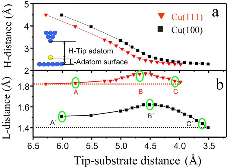
To obtain a physical understanding of the structural sensitivity, we have modelled at first the atomic relaxation in the single Co atom junction under the influence of the tip proximity and then considered its consequence on the electronic structure. Indeed, reducing the tip-substrate separation can induce a local perturbation in the atomic ordering at the junction which can affect the coupling between the orbitals of the electrodes and of the Co atom and consequently the electronic and the magnetic properties of the system. To simulate the nanoscale-junction on the atomic scale, we have performed molecule static (MS) calculations with many-body interatomic potentials levanov00 . In these simulations the tip has been represented as a pyramid consisting of 10 Cu atoms arranged in fcc(111) stacking. Figure 2 shows the variation of the tip-adatom and the adatom-substrate separations during the tip displacement (panel a and b, respectively). On a first glance one can see that beside an initial region, the tip- Co atom as well as the Co atom-substrate distances are not linearly proportional to the tip displacement. As the tip-substrate distance is reduced, the atomic order at the junction relaxes: the atoms of the tip, the Co impurity as well as the atoms of the substrate move to new equilibrium positions. The real tip-substrate distance is then a dynamic variable according to the specific location of the tip and to its attractive and repulsive interaction with the surface and the impurity. Specifically, up to the minimum distance of 5.3Å, the tip-Co atom distance is almost linear with the tip displacement. Approaching further, the distance between the opposite sides of the nanometer scale junction is reduced to a larger extend than the effectively applied tip displacement due to an attractive interaction (up to 4.7Å). Reducing the tip-substrate distance below 4.7Å, the interaction becomes repulsive. At this tip proximity, the adatom-substrate distance, defined as the vertical distance between the Co adatom and its first nearest neighbor, is strongly reduced while the distance between the tip and adatom is only slightly decreased. This implies that the Co adatom shifts towards the substrate. As a consequence when the point contact configuration is reached, the Co-Cu(111) surface distance compares to the equilibrium distance predicted for the tunneling condition (dotted line in panel b).
Figure 2 compares also the atomic relaxation process on the two copper surfaces. The general trend of attractive and repulsive interaction of tip-atom and surface can be observed in both cases. However, differences in the atom dynamics under the influence of the tip and in the Co-surface distance are obvious. Specifically, under the influence of the tip the Co impurity is pushed deeper into the Cu(100) surface in point contact configuration than it is in tunneling conditions (black dotted line in panel b). Therefore, it can be expected that the stronger interaction with the surface increases on the Cu(100) substrate the hybridization of the d-levels of the Co adatom with the sp states of the surface.

This and its consequence on the magnetic properties of the junction at various tip proximity, can be understood calculating the local density of states (LDOS) of the Co adatom. All the calculations were performed within the linear combination of atomic orbital (LCAO) formalism by means of density functional theory (DFT) implemented in SIESTAsoler02 . The geometry was optimized by SIESTA until all residual forces on each atom are smaller than 0.01eV/Å MD-Sie ; siesta .
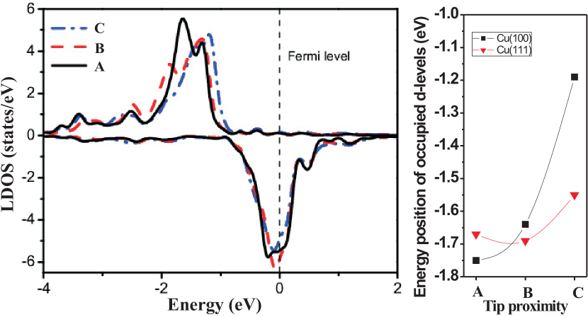
In figure 3 the d-levels of Co/Cu(111) is shown for different tip-substrate separations (denoted A, B and C in figure 2) with the energies given with respect to the Fermi level. It can be seen that only the occupied density of states of the Co adatom on Cu(111) are slightly affected by the tip substrate distance. Moreover, the energy difference between the center of the occupied spin-up band (or majority states) and the center of the partially unoccupied spin-down band (or minority states) U for three tip-substrate separations are nearly the same. Consistently, also the magnetic moment of the Co adatom at these three tip-substrate separations (1,99, 1.96 and 1,78, respectively) are only slightly affected by the tip proximity. On the contrary a large energy shift of the d-levels was reported for Co adsorbed on Cu(100) surface neel07 ; huang06 . A comparison of the energy position of the occupied d-levels is shown in figure 3b. On both surfaces the position of the occupied d-levels shifts towards higher energies under the influence of the tip proximity. On Cu(111) surface this shift is, however, much smaller. On Cu(100) the substantial change in the occupation of the d-levels is reflected in the increase of the Kondo temperature in point contact. Accurate calculations of the expected increase of the Kondo temperature on the these surfaces is, however, not straight forward. Nonetheless, the theoretical predictions and the experimentally observed Kondo temperature in point contact regime follows the trend described by the model proposed by Wahl et al. wahl04 for the tunneling regime. The increase of the occupation of the d-level effects sensibly the Kondo temperature on Cu(100) and almost negligibly on the Cu(111) surface.

In conclusion, the present experimental and theoretical work demonstrates that the local atomic geometry plays a major role in the electron transport properties of nanoscale junctions. The tip proximity in the point contact regime influences the atomic relaxation in the single atom junction and thereby determines the lattice equilibrium position. These structural relaxations induce a modification of the sp-d hybridization between the electrode surface and the bridging atom. While on the closed packed Cu surface the impurity d-level is less affected, it shifts substantially on the open (100) surface. This explains the striking difference observed in the behavior of the Kondo temperature of Co adatoms upon point contact formation on Cu(111) and Cu(100). We believe that these results have general validity and might clarify a few of the uncertainties in the electron transport through nanometer scale junctions characterized by break-junction experiments.
We acknowledge P.Wahl for fruitful discussions. The work was supported by Deutsche Forschungsgemeinschaft (DPG SPP 1165, SPP 1243 and SSP 1153)
References
- (1) G.Cuniberti, G.Fagas, K.Richter, Introducing Molecular electronics, Lecture notes in Physics 680, Springer Verlag (2005).
- (2) Kun Tao, V.S. Stepanyuk, P.Bruno, D.I. Bazhanov, V.V. Maslyuk, M. Brandbyge, and I. Mertig, Phy. Rev. B 78 014426 (2008)
- (3) E. Scheer, N. Agraït, J. Cuevas, A. Levy Yeyati, B. Ludophk, A. Martin-Rodero, G. Rubio-Bollinger, J. van Ruitenbeek, and C. Urbina, Nature 394, 154 (1998).
- (4) A. Yanson, G. Rubio-Bollinger, H. Van den Brom, N. Agraït, and J. Van Ruitenbeek, Nature 395, 783 (1998)
- (5) J. Pascual, J. Mendez, J. Gomez-Herrero, A. Baro, N. Garcia, U. Landman, W. Luedke, B. E.N, and H.P. Cheng, Science 267,1793 (1995).
- (6) E. Lörtscher, H.B.Weber, H.Riel, Phys. Rev. Lett. 98, 176807 (2007).
- (7) L. Bürgi, Ph.D. thesis, Lausanne (1999).
- (8) N. Néel, J. Kröger, L. Limot, K. Palotas, W. Hofer, and R. Berndt, Phys. Rev. Lett. 98, 016801 (2007).
- (9) R. Temirov, A. Lassise, F. Anders, and F. Tautz, Nanotech 19, 065401 (2008).
- (10) X.Xiao, B.Xu, N.J.Tao, Nano Lett. 4, 267 (2004)
- (11) H.Park, A.N.Pasupathy, J.I.Goldsmith, C.Chang, Y.Yaish, J.R.Petta, M.Rinkoski, J.P.Sethna, H.D.Abruna, P.L.McEuen, D.C.Ralph, Nature 417, 722 (1999)
- (12) J. Gimzewski and Möller, Phys. Rev. B 36, 1284 (1995).
- (13) V. Madhavan, W. Chen, T. Jamneala, M. Crommie, and N. S. Wingreen, Science 280, 567 (1998).
- (14) P. Wahl, L. Diekhöner, M.A. Schneider, L. Vitali, G. Wittich, and K. Kern, Phys. Rev. Lett. 93, 176603 (2004).
- (15) N. Knorr, M.A Schneider, L. Diekhöner, P. Wahl, and K. Kern, Phys. Rev. Lett. 88, 096804 (2002).
- (16) R. Huang, V.S. Stepanyuk, A. Klavsyuk, W. Hergert, P. Bruno, and J. Kirschner, Phys. Rev. B 73, 153404 (2006).
- (17) U. Fano, Phys. Rev. 124, 1866 (1961).
- (18) N. Levanov, V.S. Stepanyuk, W. Hergert, D. Bazhanov, P. Dederichs, A. Katsnelson, and C. Massobrio, Phys. Rev. B 61, 223 (2000).
- (19) J. M. Soler, E. Artacho, J. Gale, A. Garcia, J. Junquera, and D. Ordejon, and P. Sanchez-Portal, J. Phys. Condens. Matter 14, 2745 (2002).
- (20) LDA approaches have been used for the exchange and correlation potential, and a 250 Ry energy cutoff is used to define real-space grid for numerical calculations involving the electron density. Core electrons of all elements are replaced by nonlocal norm-conserving Troullier-Martins pseudopotentials. Valence electrons of the Cu substrate are described using double- plus polarization atomic orbital basis set, and a triple- plus polarization atomic orbital basis sets for Co adatom.
- (21) We chose three different tip-substrate distances (denoted A, B and C in figure 2) and perform a fully relaxation by Siesta code. The displacements of the Co adatom at three tip-substrate separations (denoted , and in Fig. 2) calculated by the MS method are 0.02Å, 0.21Å and 0.05Å, respectively. While these are 0.01Å, 0.26Åand 0.08Å obtained from Siesta code, coinciding with the MD results very well. Relaxation of the atoms in the tip is also taken into account in our calculations huang06 .