Parity-dependent proximity effect
in superconductor/antiferromagnet heterostructures
Abstract
We report the effect on the superconducting transition temperature () of a Nb film proximity coupled to the synthetic antiferromagnet Fe/Cr/Fe. We find that there is a parity dependance of on the total number of Fe layers, ; locally is always a maximum when is even, and a minimum when is odd. The Fe electron mean free path and coherence length are indicative of dirty limit behavior; as such, we numerically model our data using the linearized Usadel equations with good correlation.
pacs:
74.45.+c, 74.62.-c, 74.78.DbDuring the past fifteen years the coupling of thin film superconductors (S) to ferromagnets (FM) Review has been extensively studied. In the most simplistic sense, these electron coupling phenomena can be considered to be mutually exclusive with spin alignment enforced by ferromagnetic exchange and anti-parallel spin alignment necessary for singlet BCS superconductivity. According to theory, the penetration depth of the superconducting proximity effect (SPE) into normal metals (NM) is governed by the electron phase breaking length. When NM is substituted with a FM, the singlet superconducting correlations and phase coherent effects are destroyed by the exchange interaction within the FM coherence length because of the splitting of spin-up and spin-down conduction bands. For S/FM bilayers, a consequence of on S is the non-monotonic dependence of on FM layer thickness () for when the superconductor is thinner than its BCS coherence length Jiang1995 . This can be understood in terms of an interference effect between the transmitted singlet pair wave function through the S/FM interface with the wave reflected at the opposite FM interface.
Recently, Andersen et al. Andersen predicted a SPE dependence on the number of antiferromagnetic (AF) atomic planes () in S/AF/S junctions such that the junction’s ground state is or depending on whether is even or odd. Experimentally, this SPE dependence on is difficult to realize because it demands atomic thickness control of the AF. So far, experiments looking at the proximity of S to AFs have focused on thicker AF layers SAFS where this parity dependence does not exist. A way to investigate a parity dependent SPE is to use synthetic antiferromagnets (SAFs) which exploit the AF coupling of FM layers separated by a NM spacer ParkinPRL6423041990 .
So far, the proximity effect of SAFs coupled to S materials have not been considered although the dependence of complicated multilayers have been extensively studied FeMulti ; for example, the control of in pseudo-spin valve FM/S/FM structures has been proposed PSVTHEORY and realized experimentally PSV with mK differences in between parallel (P) and anti-parallel (AP) FM configurations. The most similar structure to the one we study here was proposed by Oh et al. Sangjun in which the S layer is in proximity to decoupled FM/NM/FM. In this Letter, we report the proximity-suppression of of a Nb film coupled to a Fe/Cr/Fe SAF. In doing this, we find that has a pronounced parity dependence on such that when is even, is a local maximum and, conversely, when is odd, is a local minimum.
Films were grown in Ar (1.5 Pa) on oxidized (120 nm) Si (100) (surface area: 5-10 mm2) in a diffusion-pumped ultrahigh vacuum sputter deposition system, consisting of the following: three dc magnetrons; a computer operated (rotating) sample table; a liquid N2 cooling jacket; and a residual gas analyzer. The vacuum system was baked-out overnight prior to each experiment, reaching a base pressure of 1-410-6 Pa. One hour before depositing, the system was cooled with liquid N2 giving a final base pressure of 1-310-8 Pa, a residual pressure of 410-9 Pa, and an outgassing rate of 110-8 Pa s-1. Targets (Nb, Fe, and Cr of 99.9 purity), were pre-sputtered for 15 minutes to remove contaminants from their surfaces and to further reduce the base pressure of the vacuum chamber by getter sputtering. To control film thickness () and to ensure clean interfaces, films were grown in a single sweep by rotating the substrates around the symmetry of the chamber under stationary targets. Growth rates were pre-calibrated by growing films on patterned substrates and, from a lift-off step-edge, for each material was established using an atomic force microscope. Typical growth rates with a sweep speed of 1 rpm per pass were: 1.0 nm for Cr; 0.6 nm for Fe; and 1.4 nm for Nb. The average film roughness was 3 Å over 1 m.
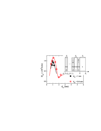
The antiferromagnetic interlayer exchange coupling (AFC) between the Fe layers was investigated in two sets of Nb/Fe/Cr/Fe films: for =0.6 nm; and for =1.0 nm. was constant (20 nm) while varied in the 0.5-2.5 nm range. A 2.8 nm capping layer of Nb was grown on the top Fe layer. To quantify AFC in these films and to optimize to give the largest AFC energy (given by where is the magnetization of the Fe), the required saturating field needed to align the Fe layers was measured with a vibrating sample magnetometer at room temperature as a function of ; see Fig.1. For 0.6 nm, is a maximum value of (1.160.04) A/m for 1.0 nm with 0.8106 A/m (similar to Robinson2007 ). This corresponds to 1.810-4 Jm-2, which compares well to previously reported energies ParkinPRL6423041990 . To achieve the most efficient AFC, we chose 0.6 nm and 0.9 nm for the appropriate layer thicknesses.
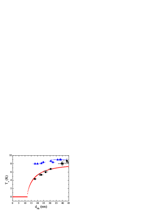
To establish a range that is strongly affected by the presence of the SAF film, the of both bare Nb and Nb/Fe/Cr/Fe films was measured in the 15-45 nm range; see Fig. 2. The critical is 12 nm. was estimated by measuring the resistance of a film as a function of temperature () using a standard four contact technique; for this, two instruments were used: a custom made liquid He dip probe and a pumped He-4 temperature insert. To make electrical contacts, films were ultrasonically wire-bonded onto copper carriers with Al wire (25 m diameter). Samples were fixed to their carriers with silver conducting paint. An ac current of 10A was applied. was estimated from warming curve data and defined as the mid-point of the transition.
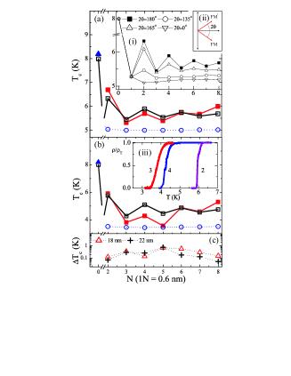
Fig. 3 shows the dependence of on for two Nb thicknesses: (a) 22 nm and (b) 18 nm. We see that is a local maximum when is even and vice-versa. The magnitude of decreases as increases: the largest for 1.38 K in (a) and 2.06 K in (b). Assuming dirty limit behaviour in the multilayers (), we have adapted the Usadel equations, as discussed by Fominov et al. FominovPRB660145072002 and Oh et al. Sangjun , to model the situation; as illustrated in the inset of Fig. 1.
The normal Green function is when and the linearized Usadel equations for the anomalous Green function are:
| (1) |
inside the S layer,
| (2) |
inside the th () FM layer and
| (3) |
inside the th () NM layer.
The appropriate diffusivities are , and , while is the superconducting pairing potential in the S layer. The factor before accounts for the alternating polarization of the FM layers. The Usadel equations are supplemented by the self-consistency equation
| (4) |
where the summation goes over the Matsubara frequencies with all integers . is the of bare S of thickness , i.e. see Fig.2. The anomalous function obeys the boundary conditions
| (5) |
at the points separating any and layers; and can be either of the S, FM or NM layers and in each case we use the appropriate normal-state conductivities ( and ) as well as the appropriate interfacial resistance per unit area between and layers. Since all the FM and NM layers are identical, the three conductivities are , and and the two interfacial resistances are and .
If we introduce the formal vector , we can turn Eq. (2) and (3) into vector equations for ( refers to an arbitrary layer again), which take the common form
| (6) |
where the values of are
| (7) |
in the th FM and the th NM layers, respectively. Eq. (6) is a simple linear differential equation. If is known at the left side () of a layer, its value at the right side () can be expressed in terms of matrix exponentials
| (8) |
The boundary conditions (Eq. 5) between any two layers and can be written in the vector form as
| (9) |
The derivative of the anomalous function vanishes at the left end of the multilayer, therefore , where is a complex number. The formal vector at the left side of the S layer is now expressed in the function of by systematically going through the layers and using the appropriate matrices appearing in Eqs. (8) and (9):
| (10) |
| (11) |
is a complex matrix only dependent on material parameters and the Matsubara frequency , which depends on .
To obtain , we apply the multimode method developed by Fominov et al. FominovPRB660145072002 . If we write down the components of the vector Eq. (10) and eliminate , we obtain
| (12) |
which is analogous to Eq. (8) in FominovPRB660145072002 . From here, the problem is reduced to finding the highest for which the determinant of a matrix is zero. If we include modes () in addition to the single-mode method and take the first Matsubara frequencies (), the elements of are
| (13) |
| (14) |
where is given by
| (15) |
in the function of and . The quantities and () are the smallest positive roots of
| (16) |
| (17) |
which are obtained from the self-consistency Eq. (4) and contain the digamma function .
Using this method, we determine numerically; the calculation is repeated with various values of , for . By obtaining the roots and of Eqs. (16) and (17), and evaluating through Eq. (15), the matrix can be found for all . The largest value of for which corresponds to . The multimode method with is exact but in most cases the inclusion of 8 modes suffices.
To apply this numerical method with the minimum number of adjustable parameters, we have measured for Nb, Fe and Cr thin films for 10 K to be 1.9106 , 6.6106 , and 2.2106 , respectively. From these values, we estimate the electron mean free paths of Fe and Cr via with the Fermi velocity; for Fe Covo and Nb Finnemore is taken from literature, while for Cr we assume a similar to Fe. The density number of electrons is with the electron mass, giving an of 2.7 nm and 0.9 nm for Fe and Cr, respectively. For Nb, we determine by choosing a value that gives the best fit (2.2 nm). With known, we calculate for Nb, Fe, and Cr via , giving 2.210-4 for Nb, 1810-4 for Fe, and 6.010-4 for Cr. Finally, we estimate the coherence lengths of Nb and Cr with , giving 5.8 nm for Nb (similar to CoherenceLengNb ) and 9.6 nm for Cr, while for Fe , giving 3.7 nm (similar to Robinson2007 ) assuming 1000 K Kittel . For both Nb and Fe, , which is indicative of dirty limit behavior and, therefore, justifies our use of the linearized Usadel equations. For the interfacial resistances we take 10-15 and 10-17 (the quality of the fit does not depend strongly on these parameters). The important material parameters used/calculated here are listed in Table 1. With these values, the numerical model agrees well with the experimental data; see Fig. 3.
We have generalized the model to consider the behavior when the Fe layers are non-collinear; we use the linearized Usadel equations containing both the singlet and triplet components of the anomalous Green function Houzet2007 . We find that with a small change in , the angle between the polarizations of adjacent Fe layers, the is more strongly reduced and the parity dependent oscillations fade away faster; see Fig. 3(a,i). In the limiting case of we recover the SAF behavior. An applied magnetic field will produce a non-collinear configuration; however, in our samples this could not be achieved without directly suppressing the Nb . With improved control of the field required to reorient the layers could be substantially reduced.
In conjunction with the experimental results, this demonstrates that a large change in can be obtained by switching the SAF between P and AP configurations. In the particular case of 2, which corresponds to the Oh et al. Sangjun spin valve, the change in from AP to P is 1 K, which is a many times higher than the changes experimentally observed in the analogous superconductor PSV structures PSV .
This Letter has shown that the parity of AFs with perfect order have a profound effect on the proximity effect as predicted by Andersen et al. and that the results can be well described by the adaptation of the linearized Usadel equations to this new situation. However, there are important aspects of the results which are not explained on this basis. Firstly, there appears to be a longer period oscillation in , which is visible in both data sets as an upturn in the trend in for 5. Perhaps, more significantly, there appears to be a parity-dependence of the resistive transition width () as shown in Fig. 3(c), which suggests that the nature of the superconducting transition is being affected.
| D | ||||||
|---|---|---|---|---|---|---|
| nm | 106 ms-1 | K | 106 | m2s-1 | nm | |
| Nb | 5.8 | 0.3 | 1.9 | 2.2 | 2.2 | |
| Fe | 3.7 | 2.0 | 1000 | 6.6 | 18 | 2.7 |
| Cr | 9.6 | 2.0 | 2.2 | 6.0 | 0.9 |
This work was supported by EPSRC UK. We thank Professor James Annett
for theoretical discussions.
References
- (1) For reviews: A. I. Buzdin, Rev. Mod. Phys. 77, 935 (2005); F. S. Bergeret, A. F. Volkov, and K. B. Efetov, Rev. Mod. Phys. 77, 1321 (2005).
- (2) J. S. Jiang et al., Phys. Rev. Lett. 74, 314 (1995).
- (3) Brian M. Andersen et al., Phys. Rev. Lett. 96, 117005 (2006).
- (4) C. Bell et al., Phys. Rev. B 68, 144517 (2003); Y. Cheng and M.B. Stearns, J. Appl. Phys. 67, 5038 (1990).
- (5) S. S. P. Parkin et al., Phys. Rev. Lett. 64, 2304 (1990).
- (6) P. Koorevaar et al., Phys. Rev. B 49, 441 (1994); T. Mühge et al., Phys. Rev. Lett. 77, 1857 (1996); M. Vélez et al., Phys. Rev. B 59, 14659 (1999).
- (7) P. G. de Gennes, Phys. Lett. 23,10 (1966); L. R. Tagirov, Phys. Rev. Lett. 83, 2058 (1999); A. I. Buzdin et al., Europhys. Lett. 48, 686 (1999).
- (8) Ion C. Moraru et al., Phys. Rev. Lett. 96, 037004 (2006); J. Y. Gu et al., Phys. Rev. Lett. 89, 267001 (2002); A. Potenza and C. H. Marrows, Phys. Rev. B 71, 180503(R) (2005).
- (9) Sangjun Oh et al., Appl. Phys. Lett. 71, 2376 (1997).
- (10) J. W. A. Robinson et al., Phys. Rev. B 76, 094522 (2007).
- (11) Ya. V. Fominov et al., Phys. Rev. B 66, 014507 (2002).
- (12) M. K. Covo et al., Phys. Rev. ST Accel. Beams 9, 063201 (2006).
- (13) D. K. Finnemore et al., Phys. Rev. 149, 231 - 243 (1966).
- (14) A. S. Sidorenko et al., Ann. Phys. (Berlin) 12, 37 (2003).
- (15) C. Kittel, Introduction to Solid State Physics (John Wiley & Sons, Inc., New York, 1956).
- (16) M. Houzet and A. I. Buzdin, Phys. Rev. B 76, 060504(R) (2007).