Primary tunnel junction thermometry
Abstract
We describe the concept and experimental demonstration of primary thermometry based on a four probe measurement of a single tunnel junction embedded within four arrays of junctions. We show that in this configuration random sample specific and environment-related errors can be avoided. This method relates temperature directly to Boltzmann constant, which will form the basis of the definition of temperature and realization of official temperature scales in the future.
Temperature is a relatively poorly known quantity in modern metrology. It is well recognized that the way the international temperature scale is currently realized, in particular towards low temperatures, needs to be seriously reconsidered. It is currently based largely on artefacts which should be replaced by methods relating to thermodynamic temperature via Boltzmann constant fellmuth ; casa . Methods based on solid state tunnel junctions, Coulomb blockade thermometry (CBT) cbt94 ; bergsten99 and shot noise thermometry (SNT) spietz03 ; spietz06 , have both shown great promise as -based thermometers for metrology. However, both of them fall short up to now, when it comes to sufficient absolute accuracy. In case of SNT, the limitations are mainly of practical nature, and can possibly be overcome by a careful design of the sensor and the measurement set-up. For CBT, an uncontrolled error source is of more fundamental concern: CBT involves a measurement of a series connection of nominally identical junctions. The inevitable spread in junction parameters leads, however, to an error, which can usually be made small, but which limits the accuracy in particular when the average junction size is small hirvi95 ; farhangfar97 . In this letter we introduce and demonstrate a method, single-junction thermometry, SJT, which combines the advantages of basic CBT thermometry, but which avoids the parameter dispersion induced errors altogether. We show theoretically that the errors can then be efficiently suppressed, and demonstrate the operation in experiment.
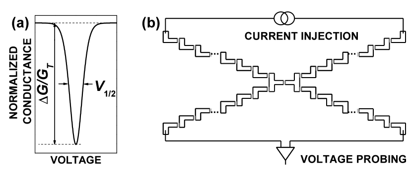
In Coulomb blockade thermometry an array of tunnel junctions shows a drop in its differential conductance around zero bias voltage, because of the influence of single-electron charging effects. The ideal operation regime of a CB thermometer is determined by the ratio of the single-electron charging energy, , where is the (average) junction capacitance, and the thermal energy at temperature such that . The measured conductance peak [see Fig. 1(a)] has two important characteristics, its full voltage width at half minimum, , and its normalized (by asymptotic conductance at large voltages, ) depth . Here the first one is given by per junction, and serves as the primary thermometer, provided the junctions in the sensor are mutually identical. The latter one is inversely proportional to . SJT thermometry is based on the same principle as CBT but there the objective is to measure the conductance of a single tunnel junction, embedded in a four probe configuration through lines consisting of arrays of tunnel junctions, see Fig. 1(b). In this topology, the advantageous protection from the influence of electromagnetic environment is achieved. At the same time, this configuration abolishes any requirement of a uniform structure, because only one junction is probed, and the rest of the junctions, indeed not necessarily identical, act as an environment for this one.
We separate the theoretical analysis into two parts. First we consider the case where the influence of the environment beyond the junction array can be neglected. We show that the measurement is perfect in this case even for a non-uniform structure. Then we use this result as the seed for analyzing the influence of the dissipative environment on the performance of the thermometer, and show that with sufficiently long junction arrays the accuracy can be maintained at the desired level.
The tunnelling rate through a junction in forward () or backward () direction with normal conductors in thermal equilibrium is given by averin
| (1) |
where is the junction resistance, , and is the change in electrostatic energy in tunnelling. We may separate this energy change as , where is the (mean) voltage drop across junction and is the internal energy change associated with charging the capacitors of the array. In the present analysis we limit ourselves to the lowest order result in , which is what yields the basic results in thermometry. In this spirit, we then expand . Analytic corrections for lower temperatures can be obtained readily by expanding up to higher orders, but they will not be considered here. The current through junction can be obtained as . Here, is the occupation probability of the charge configuration on the islands within the array. With these premises, and by using identities and , we obtain
| (2) | |||||
The internal charging energy for each charge configuration is given by , where is the inverse capacitance matrix of the junction array. We have neglected the offset charges on the islands since in the high temperature regime the charge distribution is quasi-continuous, hirvi95 . Let us denote the islands surrounding the junction by L and R. Then for the relevant processes only changes into and to , whereas all the other charge numbers remain constant. There are two junction connections to islands L and R in SJT. Evaluating as the difference of for the charge configurations before and after the tunnelling event, and making use of the properties and for all because of the symmetry of , we obtain the normalized conductance of junction , as
| (3) |
where , and . The result of Eq. (3) is in fact the basis of the standard CBT formula in linear arrays of junctions. Equation (3) tells that conductance of a single junction in SJT is accurate as a thermometer in any array of junctions: the magnitude of conductance suppression depends on the distribution of junction sizes via the capacitance matrix (), but the temperature can be determined unambiguously from, e.g., the half width of , if can be measured. Error-free measurement of is indeed possible in the configuration of Fig. 1(b). This happens since the voltage measurement via two arrays is typically performed using an amplifier with very large input impedance (in any case much larger than the resistance of the junction arrays). Then, essentially no current flows through these two arrays, and there is no voltage drop across them. Thus is indeed the voltage seen by the amplifier.
The analysis above applies to the case where the connection to the bias sources and signal amplifiers has zero impedance. In practice this is not the case, and the environment impedance introduces errors to Coulomb blockade thermometry which can be suppressed by using long arrays of junctions farhangfar97 . Similarly, one can realize the single junction measurement which avoids the errors by the embedding arrays. To analyze the remaining errors in this case quantitatively, we may write the tunnelling rates instead of of Eq. (1) as
| (4) |
Here, originates from the environment theory of single-electron tunnelling pe , and it yields the probability (density) of electron to exchange energy when it tunnels: positive (negative) refers to energy emission (absorption) by electron. In the first analysis above we thus assumed , i.e., the Dirac delta function. The same steps as in the ideal dissipationless environment above lead now to
| (5) |
Here, . For , Eq. (Primary tunnel junction thermometry) reduces naturally to (3). Equation (Primary tunnel junction thermometry) yields an easy way to evaluate the influence of environment even in complex circuits.
In general is obtained from the phase-phase correlation function with pe . Here we assume that the array is uniform and embedded in a resistive environment with resistance . We are interested in conductance of one junction within an array. can be written as
| (6) | |||
Here , , and . For a linear array of junctions we have . The results for the corresponding SJT are identical to these upon replacing by in the expressions above. Here is the number of junctions in each of the four surrounding arrays. Above we have assumed that the stray capacitances are small.
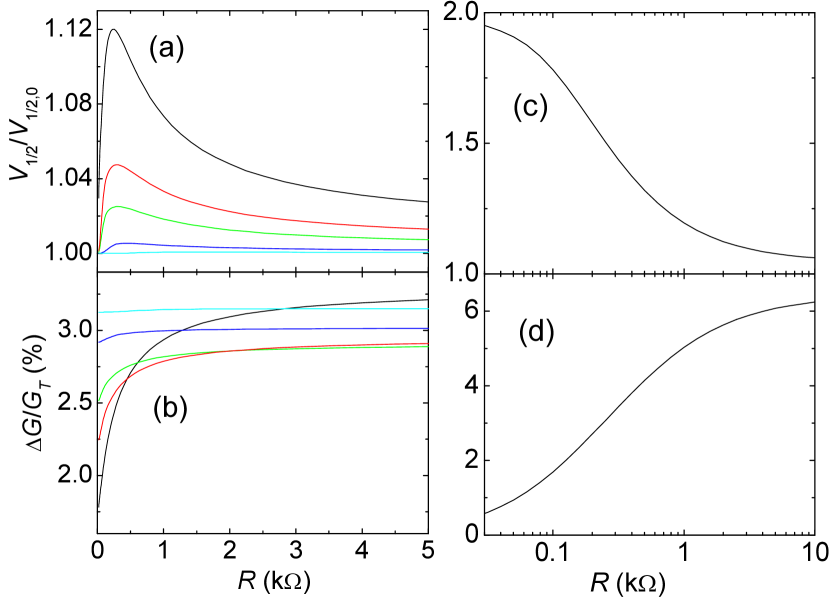
Figure 2 shows numerical results based on the analysis above. Figure 2(a) shows the width as normalized to the ideal width in delta-function environment for a junction in arrays with varying length and as a function of . It is clear that one needs to protect the junction by a long array, if accurate measurement of temperature using is to be obtained. For , an error of about 10% in the range is expected. The impedance of the environment at high frequencies is approximately , determined by the permittivity and permeability of the medium. For vacuum its value is , and for a circuit on silicon it is a few times smaller. Such increase of due to environment in short arrays is supported quantitatively by experiments, see, e.g., Ref. hirvi95 . The depth of the conductance dip is shown in Fig. 2(b): it depends strongly on only in short arrays. We note that: (i) Since the environment is never known precisely in the experiment, there is almost no way to correct theoretically for such errors: the only working strategy then is to suppress these errors precisely by embedding the measured junction in a long array. (ii) The effect of error suppression is essentially proportional to (if ). Therefore, an array with is in principle sufficient for measurements with absolute accuracy. (iii) Embedding a junction in a very resistive environment joyez97 instead of a junction array is not the best strategy in thermometry either, which is indicated by the very slowly decaying tails of the error at large values of . To fully appreciate this point, we show in Fig. 2(c) and (d) the width and depth, respectively, of a single junction peak in a purely resistive environment. Although the width at large values of slowly approaches unity, experimentally it is hard to fabricate resistive environments with k.
This concludes our proof that, theoretically, the influence of uncontrolled error sources, the inhomogeneity of the junction array and the noise of the environment, can be efficiently suppressed in a SJT. We discuss next the proof-of-the-concept experiments. Samples [see Fig. 3(a)] were fabricated by electron beam patterning and shadow angle evaporation with an oxidation step between the two electrode layers. Both the bottom and the top electrodes are of aluminium, they are 40 nm and 45 nm thick, respectively. The bottom electrode was thermally oxidized at 100 mbar for 10 min before deposition of the top electrode at an oblique angle. Two samples (A and B) with two types of structures have been measured in this work. The single tunnel junction was connected either directly to the external leads or it was embedded within four arrays of junctions, respectively. The two types of structures were fabricated on the same chip in the same vacuum cycle. Nominally, the central junctions are identical in the two cases, and all the junctions are 0.6 m2 of area, yielding a junction resistance of k (Sample A) and k (Sample B).

The samples were measured in a dilution refrigerator with a 40 mK base temperature. However, these structures were not suitable for very low temperature measurements: we observe strong self-heating due to weak electron-phonon coupling in the present geometry near base temperature meschke04 . Therefore we present here data at temperatures at and above 150 mK. Conductance measurements in the SJT configuration yield a deeper and narrower peak than for the unprotected single junction structure in agreement with the calculated results of Fig. 2. This is shown in Fig. 3(b) for Sample B. Both the SJT () and the bare junction () data follow the environment calculation assuming , a value which is consistent with the discussion above. The arrays can thus indeed be employed to efficiently protect the junctions against environment fluctuations.
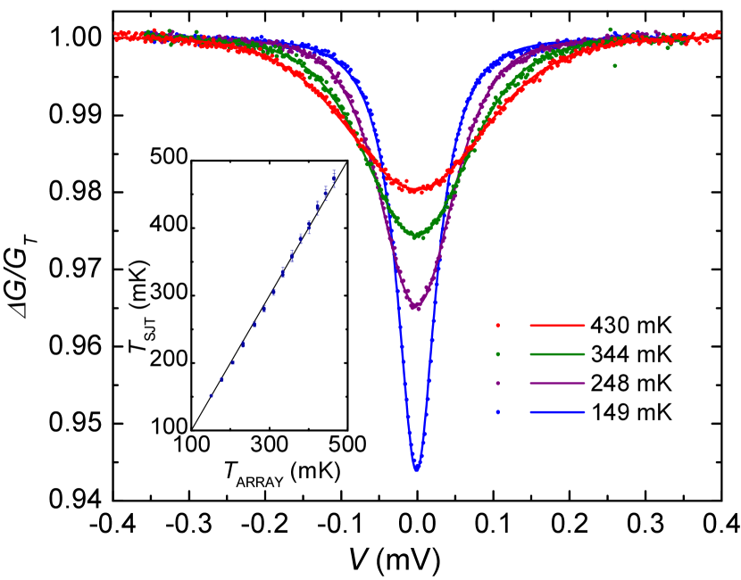
Figure 4 shows four-probe conductance measurements of the SJT sample at a few temperatures together with fits according to the model presented. We included in the fits the influence of self-heating in the manner presented in Ref. meschke04 , and this yielded perfect match to the peaks, see the lines on top of the data. The self-heating has, however, only a small influence on the curves at the temperatures shown. The extracted temperatures from such fits are shown in the inset of Fig. 4 against the reading of the CBT ”reference thermometer”, which was one of the junction arrays in the same sample. The dominating discrepancies between the two thermometers are due to finite errors in the fitting procedure in each case. The agreement between the two is good over the whole temperature range in Fig. 4.
In the theoretical analysis we focused on the high temperature and high junction resistance limit, and did not discuss errors due to, e.g., enhanced Coulomb effects at lower temperatures farhangfar97 and strong tunnelling in low resistance junctions averin92 ; farhangfar01 . Yet these errors can be treated similarly to what has been done in standard Coulomb blockade thermometry, and their influence can be estimated and kept at a tolerable level by proper choice of junction sizes for each temperature and with suitable tunnel barrier parameters. One more (controllable) error to judge is the influence of the size of the islands between the junctions, : as long as it is smaller than the distance to ”horizon”, , the above lump element analysis is valid kauppinen98 ; wahlgren98 . Here, is the signal propagation speed. The condition gets critical at particularly high temperatures, and extra care to place the array close to the junction has to be taken then. We want to add that the presented thermometry is not necessarily limited to the standard planar tunnel junction design, but may be applicable, e.g., in scanning probe or break junction geometries, since the junction parameters of the surrounding arrays need not be the same as those of the central junction. This might lead to the possibility of using tunable tunnel junctions in thermometry.
Summarizing, we propose an absolute single tunnel junction thermometer. We have demonstrated the concept in preliminary experiments. Our method may turn out to be valuable in future realization of the international temperature scale based on Boltzmann constant.
We thank Mikes (Centre for Metrology and Accreditation) and NanoSciERA project NanoFridge for financial support, Dmitri Averin for a useful discussion, and Mikko Möttönen for help in the analysis.
References
- (1) B. Fellmuth, Ch. Gaiser, and J. Fischer, Meas. Sci. Technol. 17, R145 (2006).
- (2) G. Casa et al., Phys. Rev. Lett. 100, 200801 (2008).
- (3) J.P. Pekola, K.P. Hirvi, J.P. Kauppinen, and M.A. Paalanen, Phys. Rev. Lett. 73, 2903 (1994).
- (4) T. Bergsten, T. Claeson, and P. Delsing, J. Appl. Phys. 86, 3844 (1999).
- (5) L. Spietz, K.W. Lehnert, I. Siddiqi, and R.J. Schoelkopf, Science 300, 1929 (2003).
- (6) L. Spietz, R.J. Schoelkopf, and P. Pari, Appl. Phys. Lett. 89, 183123 (2006).
- (7) K.P. Hirvi et al., Appl. Phys. Lett. 67, 2096 (1995).
- (8) Sh. Farhangfar et al., J. Low Temp. Phys. 108, 191 (1997).
- (9) D. V. Averin and K. K. Likharev, J. Low Temp. Phys. 62, 345 (1986).
- (10) P. Joyez and D. Esteve, Phys. Rev. B 56, 1848 (1997).
- (11) Sh. Farhangfar, A. J. Manninen and J. P. Pekola, Europhys. Lett. 49, 237 (2000).
- (12) G.L. Ingold and Yu.V. Nazarov, in Single Charge Tunneling, NATO ASI Series B, Vol. 294, pp. 21 - 107, edited by H. Grabert and M.H. Devoret (Plenum Press, New York, 1992).
- (13) M. Meschke et al., J. Low Temp. Phys. 134, 1119 (2004).
- (14) D.V. Averin and Yu.V. Nazarov, in Single Charge Tunneling, NATO ASI Series B, Vol. 294, pp. 217 - 247, edited by H. Grabert and M.H. Devoret (Plenum Press, New York, 1992).
- (15) Sh. Farhangfar et al., Phys. Rev. B 63, 075309 (2001).
- (16) J.P. Kauppinen and J.P. Pekola, Phys. Rev. Lett. 77, 3889 (1996).
- (17) P. Wahlgren, P. Delsing, T. Claeson, and D.B. Haviland, Phys. Rev. B 57, 2375 (1998).