Metallic Pattern Fabrication in Organic Mott Insulating Crystal by Local X-Ray Irradiation
Abstract
We have fabricated a metallic structure in an organic Mott insulator -(BEDT-TTF)2Cu[N(CN)2]Cl. The periodic metallic domains of approximately 9090 m2 obtained by X-ray irradiation through a molybdenum mesh mask are visualized by scanning microregion infrared reflectance spectroscopy technique. No deterioration by irradiation is found in a range of nanometer to micrometer scales. We demonstrate that the present processing method is applicable for the fabrication of molecular electronic devices.
Organic materials have been of great interest for recent years because of its potential for the application to electronic devices such as light-emitting diodes, field effect transistor (FET), etc.[1] Their low-cost and lightweight feature is an important advantage over conventional semiconductors. However, there is a difficult problem to utilize organics for fabricating devices: softness of organics constantly interferes with assembling circuits, particularly the preparation of good electrical contact between metal electrodes and organic surface.
The most widely used molecular semiconductors, including pentacene, thiophene oligomers, and rubrene, etc., are conventional band insulators. For further performance improvement in organic electronics, Mott insulators have been the object of recent studies as a new seeding material. Molecular based charge transfer (CT) salts stand out as a good candidate for this purpose, because most of them are included in strongly correlated electron systems, exhibiting a wide variety of electronic states by controlling bandwidth or carrier density. For instance, an organic FET system using tetrathiafulvalene-tetracyanoquinodimethane (TTF-TCNQ) based Mott insulating crystals has been successfully realized[2]. One of the most vigorously investigated CT salts is so-called -type bis(ethylenedithio)tetrathiafulvalene (BEDT-TTF) family, which has various electronic states resulting from the strongly correlated electron interaction [3]. The ground state of an antiferromagnetic insulator -(BEDT-TTF)2Cu[N(CN)2]Cl varies to a superconducting state by applying small static pressure ( 300 bar) [4, 5, 6, 7]. This has been known to be a Mott insulator-to-metal transition induced by controlling bandwidth. On the other hand, carrier density is almost invariable in the CT salts because of difficulty in substituting molecules partly with different valent components[8] or synthesizing nonstoichiometric crystals except for a few cases[9, 10].
According to a recent report, X-ray irradiation into the organic Mott insulator increases electrical conductivity at room temperature (RT)[11]. Whereas the detailed mechanism of such carrier delocalization has not been clarified, a possible scenario is a kind of carrier doping to the electronic system due to local destruction of the charge balance between donor and anion molecules. Apart from attractive mechanism of controlling carrier density, here we focus on the permanent improvement of conductivity by X-ray irradiation: it can be readily applied to fabrication of metallic structures in the insulating crystal by means of spatially local irradiation, such as through mask pattern (Fig. 1(a)). We employ this method as a first step to exploit a new tool for molecular electronic device fabrication. In this letter, we fabricate a metallic structure in the Mott insulator -(BEDT-TTF)2Cu[N(CN)2]Cl by X-ray irradiation through a mesh mask. Scanning microregion infrared reflectance spectroscopy (SMIS) [12] provides imaging of the metallic domains with approximately 90 90 m2 area. There is no visible irradiation damage under optical microscope and scanning tunneling microscope (STM).
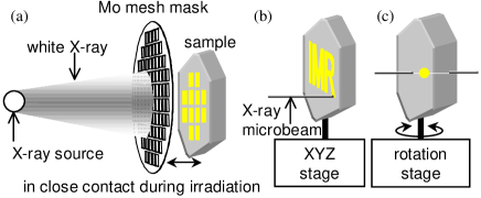
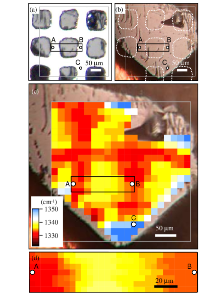
Single crystals of -(BEDT-TTF)2Cu[N(CN)2]Cl were grown by a standard electrochemical technique. The configuration for X-ray irradiation is schematically depicted in Fig. 1(a). The largest facet corresponding to the conduction layer in an as-grown crystal with dimensions approximately 0.40.30.1 mm3 was covered with a mask of molybdenum mesh sheet (with 9090 m2 mesh size, 30 m bar width, and 10 m thickness, see Fig. 2 (a)). White X-ray (40 kV, 20 mA tungsten target) was irradiated through the mask for 160 hours at RT. No other treatment on the sample surface was carried out. Figure 2(b) is a photograph taken after irradiation, indicating that there is no visible irradiation damage on the surface, while there are several inherent scratches and a large dent at the upper-right side. We performed an SMIS study[12] using a synchrotron radiation light source at SPring-8 BL43IR[15]. Each polarized reflectance spectrum was measured on the irradiated plane at 4 K with the electric field () parallel to the -axis. Whether or not a -(BEDT-TTF) ( denotes anions) is metallic is indicated by a totally symmetric intramolecular vibration mode [13] of the spectra. Since this vibration mode markedly reflects the electronic state of the conduction carrier via electron-molecular vibration coupling,[14] the frequency of the mode is sensitive to the degree of localization of the carriers; the peak frequency in a metallic state is found to be higher than that in an insulating one [13].
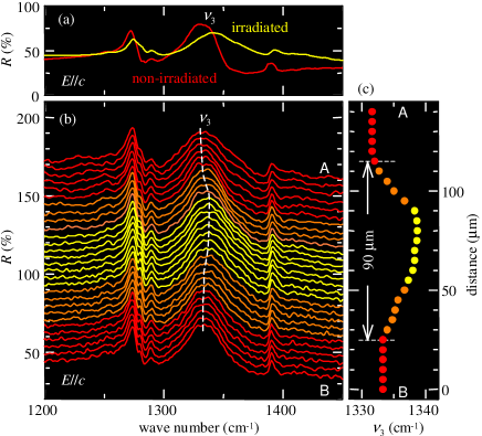
First of all, to verify this frequency shift in the present case, let us compare the polarized reflectance spectrum of a non-irradiated sample with that of an irradiated one for 325 hours. Figure 3(a) shows the reflectance spectra at 4 K with . The most remarkable peak, found at approximately 1330 and 1345 cm-1 in the non-irradiated (red curve) and irradiated (yellow) samples, respectively, comes from the phonon mode as mentioned above. The peak shift toward higher frequency by irradiation clearly demonstrates that X-ray irradiation induces the metallic state.[17] This is in good agreement with the dc resistivity data [11].
Figure 3(b) shows a spatial variation of the spectra taken at regular intervals of 5 m from point A to B (denoted in Fig. 2). Each spectrum is shifted by 4% for clarity. The peak frequency varies with position, reflecting higher frequency of the metallic sites (yellow curves) than that of the insulating sites (red curves). The peak positions of the mode represented with a broken curve are located between 1330 and 1340 cm-1, which are suitably consistent with the data displayed in Fig. 3(a).
Figure 2 (c) shows the two-dimensional map of the peak frequency of the mode over 300300 m2 area. The spectra were taken at regular intervals of 15 m. Since brighter color represents higher frequency, the mode in the yellow-to-blue colored area (1335 – 1350 cm-1) indicates the metallic state caused by X-ray irradiation. By contrast, the red area with a frequency of approximately 1330 cm-1 expresses the insulating state featuring non-irradiation. Thus the obtained image successfully describes the periodic metallic domains irradiated through the mask pattern shown in Fig. 2(a).
We next discuss the horizontal resolution of the domain edge. The spatial dependence of the peak frequency between points A and B is shown in Fig. 3(c). This indicates that the metallic region marked with the orange and yellow circles spreads over a distance of 90 m, which coincides with the mesh size of the mask. The border between metallic and insulating regions (orange circles) is in a range of 25 – 30 m. This broad interface of the metallic domain is possibly originating from diffusion of X-ray at the mask edge. Moreover, we note that the area near the sample edge has relatively high peak frequency (white-to-blue area in Fig. 2 (c)). There even exists some metallic sites regardless of its mask, for example at around point C. This out of alignment in the metallic pattern from the mask may be caused by indirect exposure of backscattering from the substrate. An effective method to improve sharpness of the boundary is to adopt other mask materials which can more effectively absorb irradiation, such as Pb or W. We therefore prepared another irradiated sample masked with a Pb plate (with 10 m thickness) on half of the sample surface. The similar SMIS measurement reveals that this yields sharper edge with a border of 10 – 20 m (not shown in Figures), which is comparable to the resolution limit of the present SMIS measurement.
It is noteworthy to comment on the vertical structure of the metallic domain. Since the penetration depth of the incident infrared light in the SMIS measurement is roughly estimated as approximately 1 m,[18] the metallic domain will have a depth of 1 m at least. Taking into account the high transmittance of X-ray, this bulky modification is reasonably accepted. However, decay of X-ray by distance may result in gradual exposure in depth direction. An extra SMIS study on the back side of the irradiated surface would give a conclusive answer to the spatial blurring in depth.
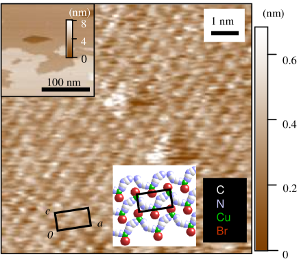
To confirm no deterioration by irradiation, an STM measurement was performed in a range of nanometer to micrometer scales. The RT-STM was carried out for an analogue sample -(BEDT-TTF)2Cu[N(CN)2]Br after 160 hours irradiation. As shown in the inset of Fig. 4, wide plateaus separated by step of approximately 4 nm are observed. This terrace structure is widely recognized in many CT salts. Moreover, the main panel of Fig. 4 shows a periodic pattern at nanometer scale, which is well consistent with the lattice constants. It should be noted that there is no remarkable difference between the STM images in the irradiated and non-irradiated samples within the present resolution.[19] An important finding from a viewpoint of application is that X-ray irradiation hardly destructs the crystal structure, implying that mechanical stability of the irradiated crystal differs little from that of the non-irradiated one.
Several practical applications of the present method can be proposed: drawing the electrical circuit by X-ray microbeam with small spot and high directivity (Fig. 1(b)), a metallic dot formation inside the insulating crystal by convergent projection of X-ray beam (Fig. 1(c)), and reforming mechanically and electronically stable interface between metal electrodes and organic crystal surface.
In conclusion, we have fabricated the metallic pattern in the Mott insulating crystal -(BEDT-TTF)2Cu[N(CN)2]Cl by means of local X-ray irradiation. The metallic domain of approximately 9090 m2 with a border width of 25 – 30 m was produced, which was successfully visualized by the SMIS measurement. No irradiation damage was observed in the STM measurement, implying the mechanical stability of the irradiated region comparable to that of the non-irradiated one. It guarantees that the present method is potentially applicable to fabricate molecular electronic devices.
The authors thank T. Hirono and T. Kawase for their technical support. Synchrotron radiation measurements were performed at SPring-8, BL43IR with the approval of JASRI (2007B1050 and 2008A1121). The research was supported by a Grant-in-Aid for Scientific Research (Nos. 16076201, 17340099, and 18654056) from the Ministry of Education, Culture, Sports, Science and Technology and the Japan Society for the Promotion of Science.
References
- [1] C. Dimitrakopoulos and P. Malenfant: Adv. Mater. 14 (2002) 99.
- [2] Y. Takahashi, T. Hasegawa, Y. Abe, Y. Tokura and G. Saito: Appl. Phys. Lett. 88 (2006) 073504.
- [3] K. Kanoda: Hyperfine Interact. 104 (1997) 235.
- [4] H. Ito, T. Ishiguro, M. Kubota and G. Saito: J. Phys. Soc. Jpn. 65 (1996) 2987.
- [5] S. Lefebvre, P. Wzietek, S. Brown, C. Bourbonnais, D. Jérome, C. Mézière, M. Fourmigué and P. Batail: Phys. Rev. Lett. 85 (2000) 5420.
- [6] D. Fournier, M. Poirier, M. Castonguay and K. D. Truong: Phys. Rev. Lett. 90 (2003) 127002.
- [7] P. Limelette, P. Wzietek, S. Florens, A. Georges, T. A. Costi, C. Pasquier, D. Jérome, C. Mézi‘ere and P. Batail: Phys. Rev. Lett. 91 (2003) 016401.
- [8] H. Mori, M. Kamiya, M. Haemori, H. Suzuki, S. Tanaka, Y. Nishio, K. Kajita, and H. MOriyama: J. Am. Chem. Soc. 124 (2002) 1251.
- [9] T. Kawamoto, T. Mori, K. Tamimiya, Y. Kataoka, Y. Aso, and T. Otsubo: Phys. Rev. B 65 (2002) 140508.
- [10] H. Taniguchi, T. Okuhata, T. Nagai, K. Satoh, N. Môri, Y. Shimizu, M. Hedo, and Y. Uwatoko: J. Phys. Soc. Jpn. 76 (2007) 113709.
- [11] T. Sasaki, H. Oizumi, N. Yoneyama, N. Kobayashi, and N. Toyota: J. Phys. Soc. Jpn. 76 (2007) 123701.
- [12] T. Sasaki, N. Yoneyama, A. Suzuki, N. Kobayashi, Y. Ikemoto, and H. Kimura: J. Phys. Soc. Jpn. 74 (2005) 2351.
- [13] T. Sasaki, I. Ito, N. Yoneyama, N. Kobayashi, N. Hanasaki, H. Tajima, T. Ito, and Y. Iwasa: Phys. Rev. B 69 (2004) 064508.
- [14] M. J. Rice: Solid State Commun. 31 (1979) 93.
- [15] Y. Ikemoto, T. Moriwaki, T. Hirono, S. Kimura, K. Shinoda, M. Matsunami, N. Nagai, N. Nanba, K. Kobayashi, and H. Kimura: Infrared Phys. Tech. 45 (2004) 369.
- [16] J. G. Analytis, A. Ardavan, S. J. Blundell, R. L. Owen, E. F. Garman, C. Jeynes. and B. J. Powell: Phys. Rev. Lett. 96 (2006) 177002.
- [17] In fact, the infrared spectrum of the irradiated sample exhibits an appearance of Drude-like structure characteristic of itinerant carriers, which will be reported elsewhere.
- [18] N. Yoneyama, T. Sasaki, N. Kobayashi, Y. Ikemoto, and H. Kimura: Phys. Rev. B 72 (2005) 214519.
- [19] As a modification by irradiation, there still remains possibility of minor structural destructions and/or local electronic variations, such as redox status of Cu atoms.