Present address: Max Planck Institute for Chemical Physics of Solids, Noethnitzer Str. 40, D-01187 Dresden, Germany ]
Direct observation of nanometer-scale pinning sites in
(Nd0.33,Eu0.20,Gd0.47)Ba2Cu3O7-δ single crystals
Abstract
We report on the observation of self-organized stripe-like structures on the as-grown surface and in the bulk of (Nd,Eu,Gd)Ba2Cu3Oy single crystals. The periodicity of the stripes on the surface lies between 500-800 nm. These are possibly the growth steps of the crystal. Transmission electron microscopy investigations revealed stripes of periodicity in the range of 20-40 nm in the bulk. From electron back scattered diffraction investigations, no crystallographic misorientation due to the nanostripes has been found. Scanning tunneling spectroscopic experiments revealed nonsuperconducting regions, running along twin directions, which presumably constitute strong pinning sites.
The practical usefulness of a superconductor depends on various properties, especially on the critical current density () and irreversibility field (). The high-temperature superconductors (HTSC) are important for future applications because the superconducting properties of these materials can be utilized at the boiling temperature of liquid nitrogen Murakami1996 . At higher temperatures, due to thermally activated depinning, flux motion appears, which is associated with an increase of electrical resistivity and energy losses Blatter1994 . Therefore, the efficient pinning of vortices at elevated temperatures is the key challenge for HTSC cuprates. For strong pinning, defects with a diameter comparable to 2 are necessary, where is the coherence length Takezawa1997 ; Sosnowski2006 . Although a normal conducting defect provides the best pinning, superconducting inclusions with modified thermodynamic properties have also been found to act as effective pinning sites, especially at elevated temperatures and/or fields Blatter1994 . By introducing secondary-phase, nonstoichiometric inclusions in the melt-processed samples, Murakami et al. achieved a significant increase of in YBa2Cu3Oy (Y-123) Murakami1989 . Even higher values have been obtained in light rare earth (LRE) compounds, especially in the ternary (Nd,Eu,Gd)-123, (Sm,Eu,Gd)-123 ones Muralidhar2003 ; Hu2005 ; Muralidhar2005 .
Recently, microstructure analysis of the melt-processed ternary LRE-123 samples showed the presence of lamellar structures of periodicity ranging from a few nm to a few tens of nm Muralidhar2003 ; Hu2005 ; Koblischka2007 . The samples showed local composition fluctuations at the nanometer scale. Single crystals, which generally offer a high morphological quality, are important for such investigations.
In this work, we report on microstructure studies on single crystals of Gd-enriched (Nd0.33,Eu0.20,Gd0.47)Ba2Cu3O7-δ (NEG-123) using atomic force microscopy (AFM), scanning tunneling microscopy (STM), transmission electron microscopy (TEM) and electron back scattered diffraction (EBSD) techniques. The goal of this investigation is to identify the potential pinning sites originated from crystal growth. A Gd-rich NEG-123 sample was chosen for this study as melt-processed samples of this type have shown pronounced stripe-like structures Koblischka2006 .
The NEG-123 single crystals were grown from self-flux using oxides and BaCO3 with purity better than 4N. Growth took place in a ZrO2/Y crucible in an atmosphere of 100 mbar of air. After growth the crystals have been oxidized in 1 bar of O2 at 698 K for 140 h and then at 667 K for 160 h. The crystals were characterized by X-ray diffraction. The unit cells are orthorhombic and the crystal is twinned. The transition temperature () as determined from the -magnetization measurements is 93.14 K (mid point of transition) with 3 K.
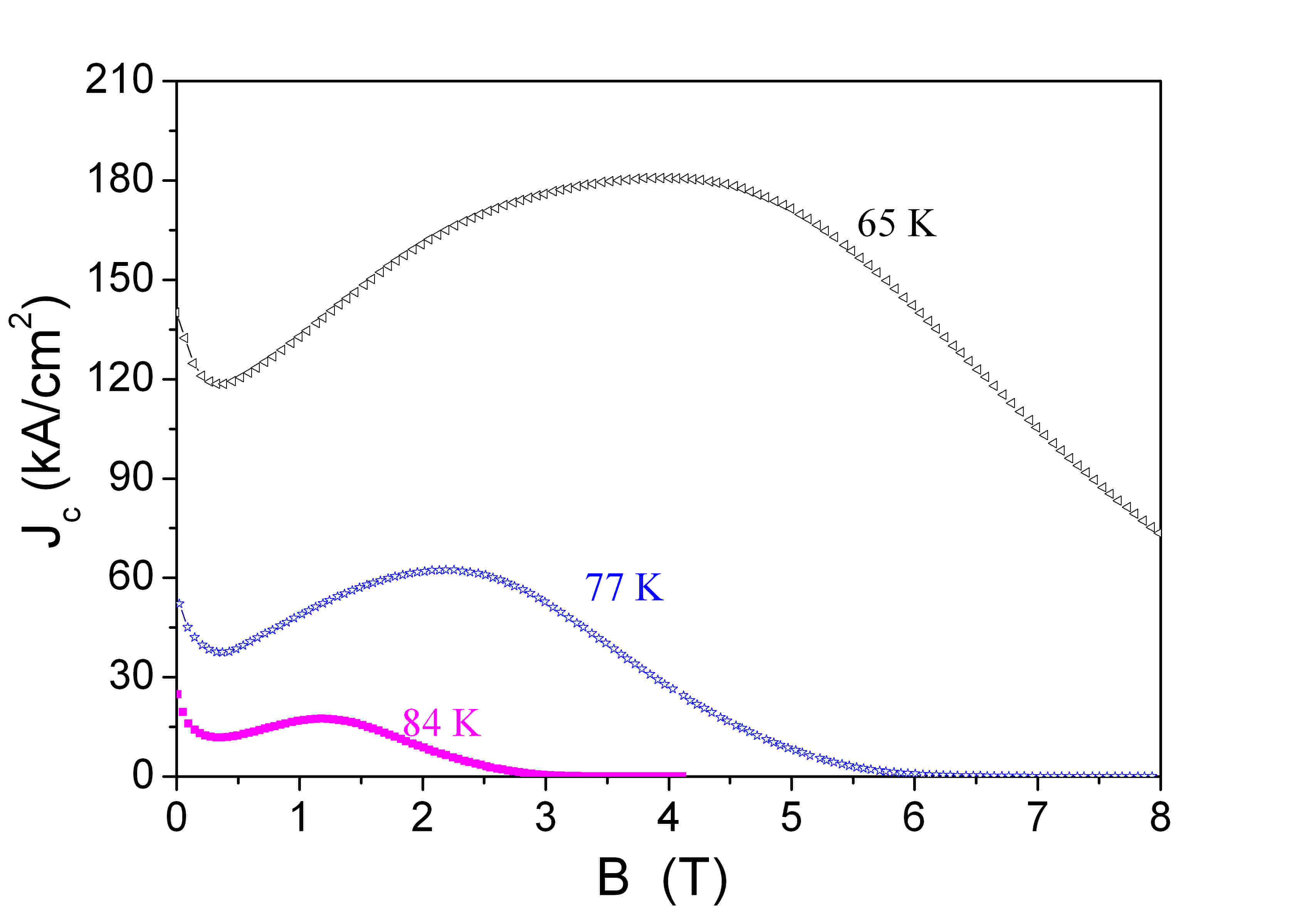
Magnetization measurements were carried out at the field sweep rate of 120 mT/s using a commercial (Quantum Design, PPMS) vibrating sample magnetometer. was calculated from the M-H loops using the extended Bean’s model formula for a sample with rectangular cross-section Chen1989 . In Fig. 1, at 65 K, 77 K and 84 K is plotted as a function of the applied magnetic field. The curves exhibit a typical fish-tail shape with strong secondary peak. With increasing temperature this peak shifts towards lower field Jirsa2007 . The secondary peak gives an evidence of an effective random point-like disorder (active at intermediate fields), similar to that in melt-processed LRE-123 samples. The solid solution of RE1+xBa2-xCu3Oy and oxygen vacancies are the sources for this type of pinning McCallum1995 . Apart from the secondary peak, another significant feature of the curves is the central peak at zero field, reaching 52 kA/cm2 at = 77 K. For the secondary peak even more than 62 kA/cm2 is observed at this temperature.
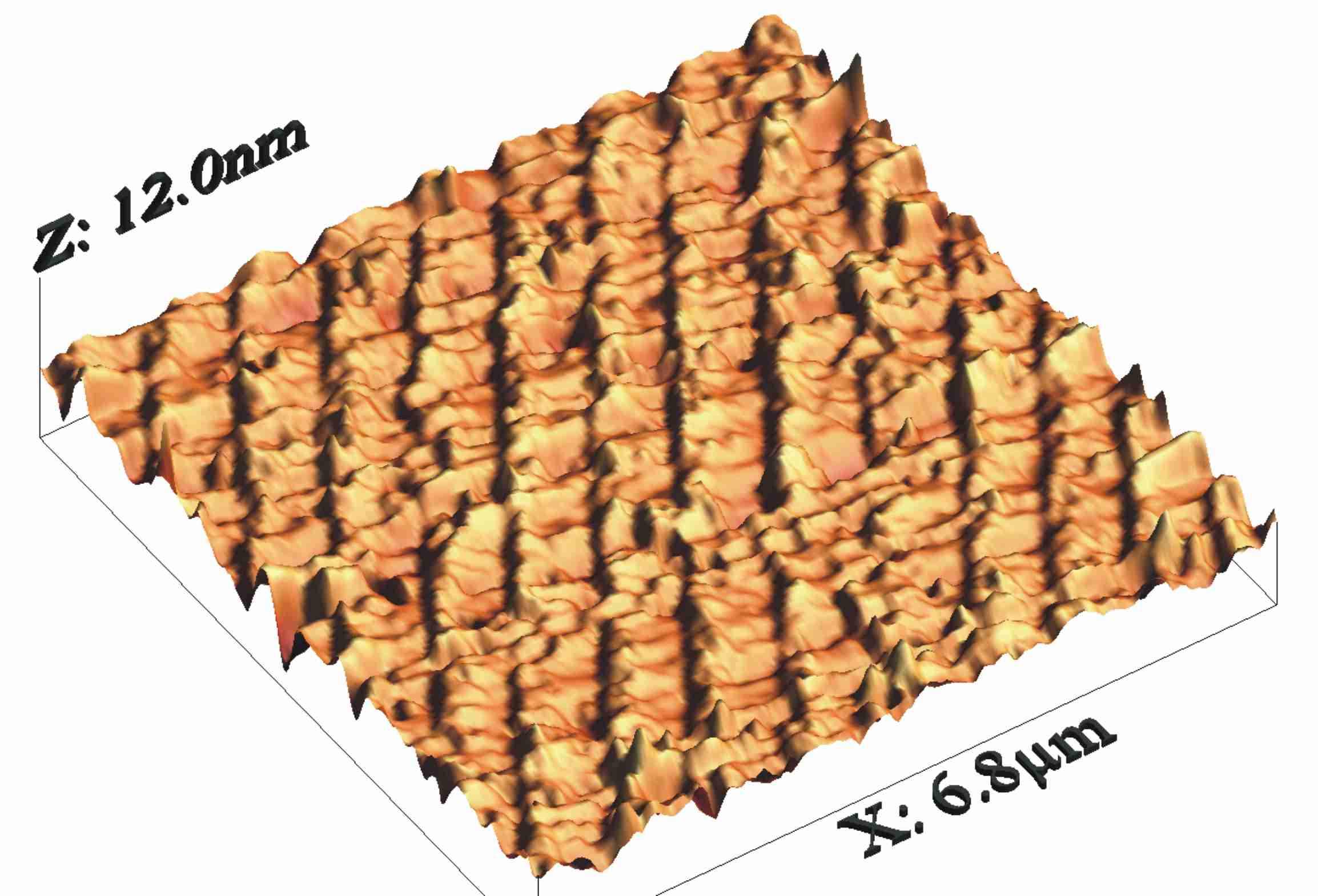
In order to identify possible pinning sites, we performed AFM studies on the as-grown sample surface. The measurements were performed at room temperature and under ambient conditions with a commercial AFM/STM (Nanoscope IV, Digital Instruments). As shown in Fig. 2, a stripe-like structure is observed. The periodicity of the stripes is in the range of 500 - 800 nm, which is an order of magnitude larger than observed for melt-processed samples Muralidhar2002 ; Koblischka2007 ; Koblischka2006 . The profile is not of lamellar form as was observed on melt-processed samples Koblischka2006 .
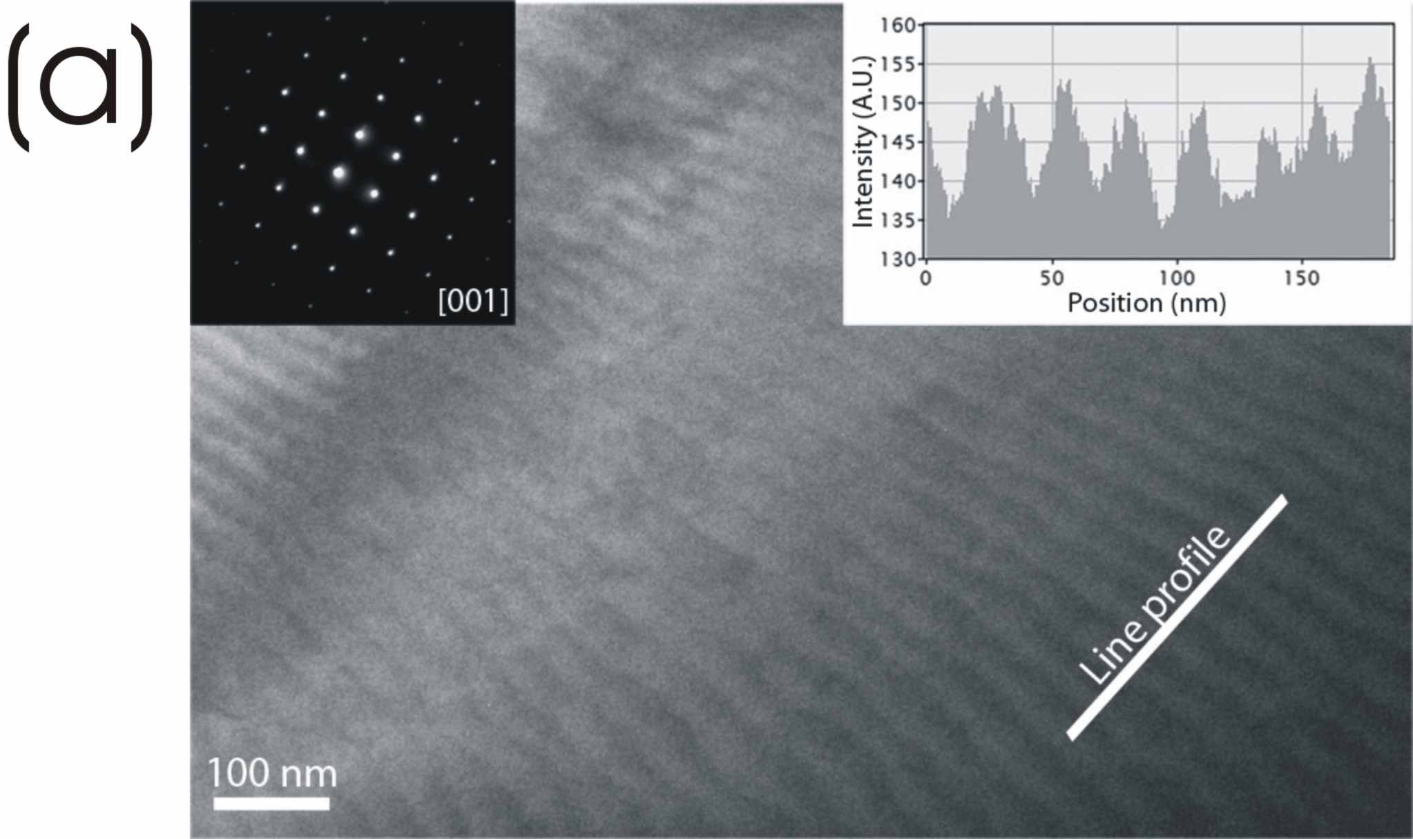
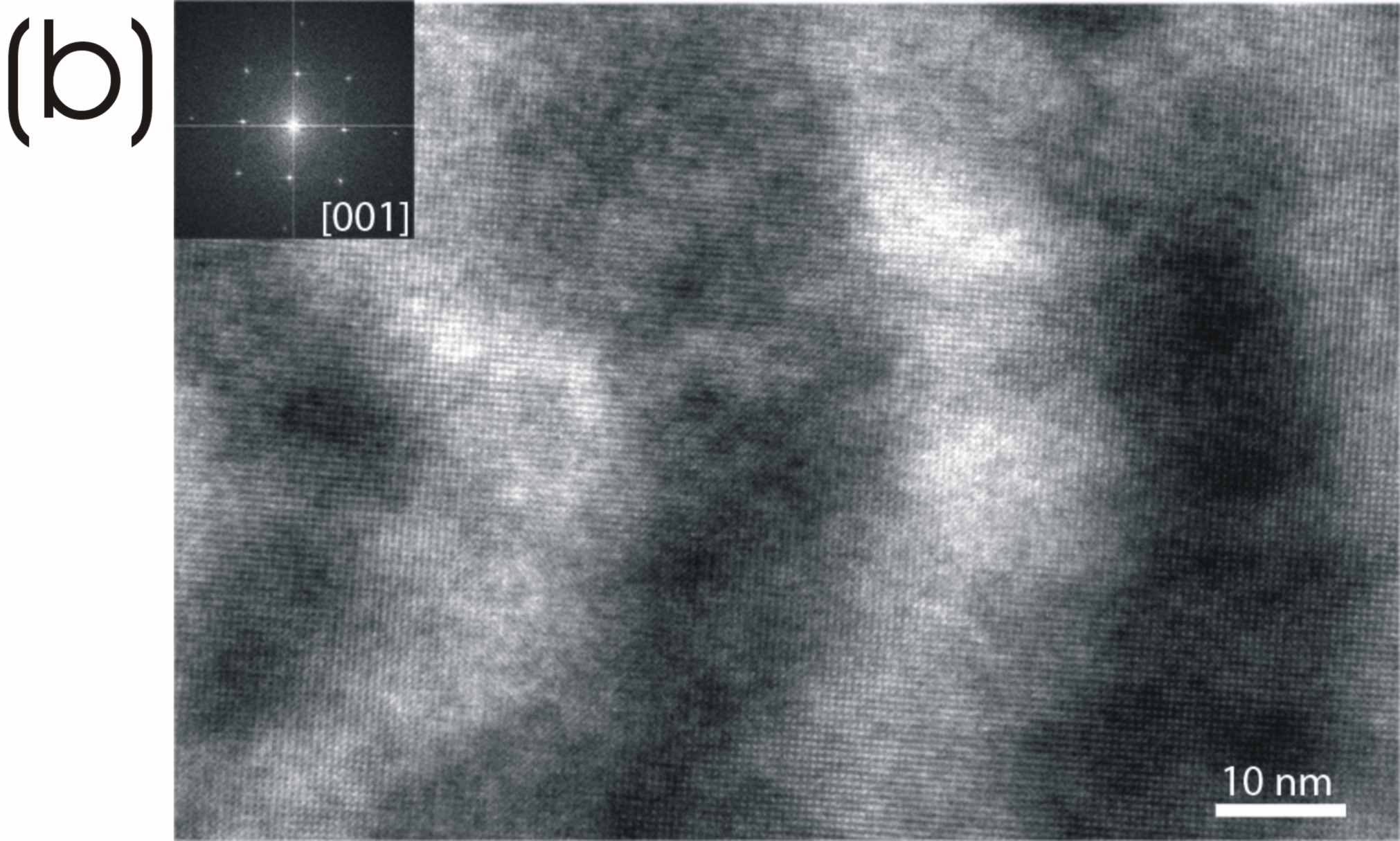
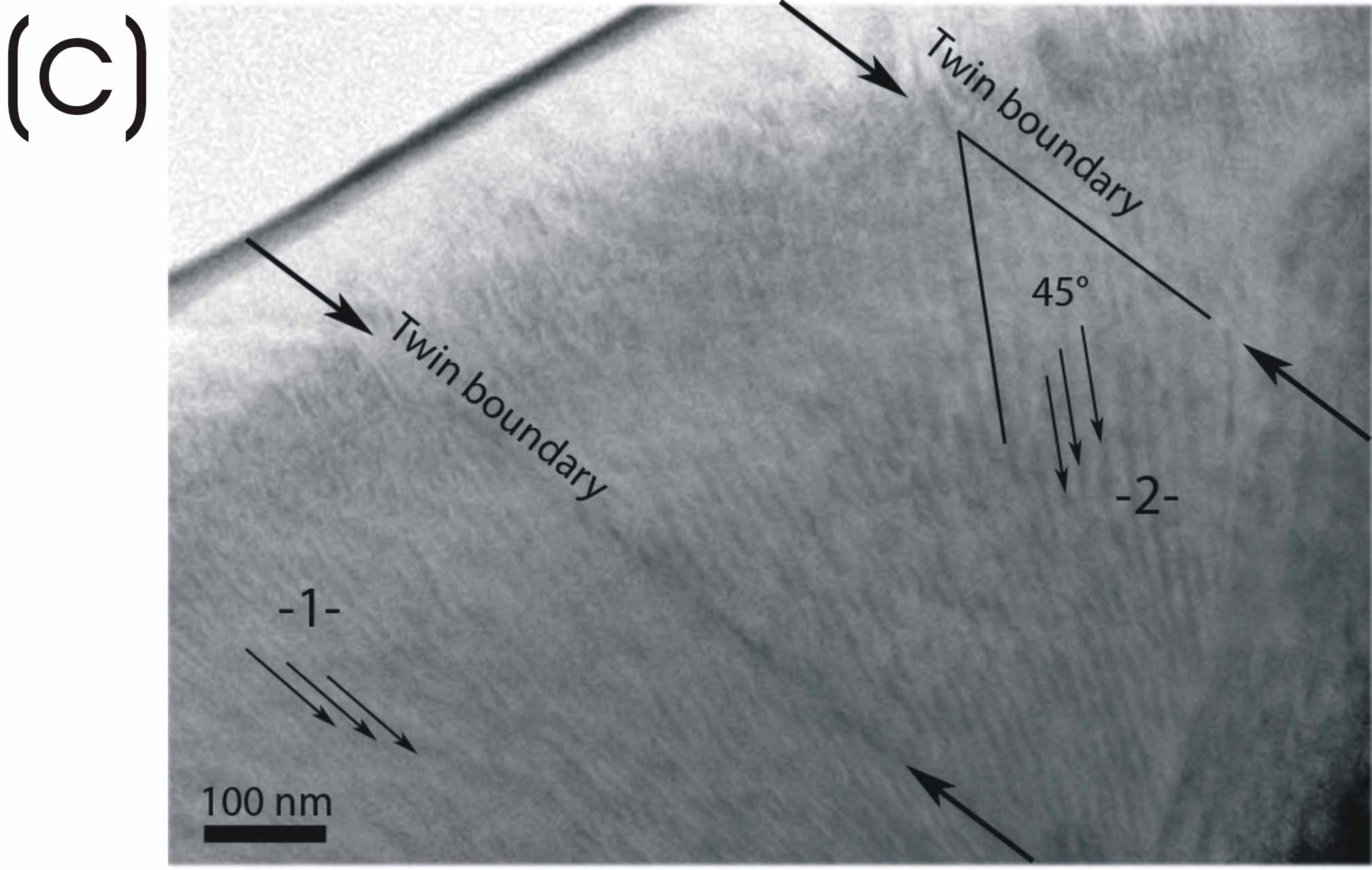
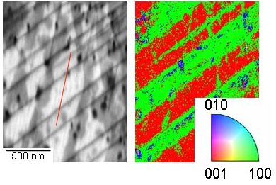
In order to elucidate if the stripes are related to vortex pinning, the microstructure in the bulk was studied by TEM using a JEOL 3000 F microscope equipped with EELS and EDX facilities. The sample was prepared by Ar ion milling. The measurements were performed along the [001] zone axis. Figure 3 shows a bright field image, exhibiting a typical pattern observed by TEM. Stripe-like features have been observed in the entire sample. The average spacing ranges from 20 nm to 40 nm (see inset of Fig. 3(a)). A typical high resolution image of the stripes is shown in Fig. 3(b). The inset fast fourier transform (FFT) shows the [001] zone axis and crystal orientation. The stripes are found to be parallel to the twin boundaries in one area (-1- in Fig. 3(c)) and inclined at an angle of 45 degrees with respect to the twin boundaries in another (area -2- in Fig. 3(c)). Thus, no clearly preferred orientation of the stripes with respect to the twins is observed. From the periodicity and topographic profile, the stripes observed in the bulk are clearly different from those observed on the surface. The latter were found to be parallel to one of the crystal edges thus being most likely growth steps. The growth-steps, generally present only on the surface Lozanne1999 , have very weak pinning performance compared to the defects in the bulk (e.g., twins) Maple2000 . Important additional crystallographic information is obtained from the image quality (IQ) map of the recorded Kikuchi pattern at each point of the sample, obtained using EBSD Koblischka2007b . The EBSD setup (TSL) is based on a FEI dual-beam workstation (see Ref. Koblischka2007 for details). Figure 4 shows the IQ map of a part of the sample and its corresponding inverse pole figure (IPF) map which reveals the crystallographic orientation. The IPF map shows that there is no crystallographic misorientation due to the nanostripes as observed for melt-processed samples Koblischka2007 .
Hu et al. suggested the stripes to originate from eutectic growth Hu2003 . Kirkaldy showed that during growth, a lamellar structure could be produced from an eutectic solution having two different phases Kirkaldy1984 . However, in the present case, crystal growth was stopped far above the eutectic temperature. Thus the proposed mechanism could not apply here. It is not known if the stripes are formed during growth or during oxygenation. The origin is very likely to be material-dependent, where the composition fluctuation plays a role, which is possibly specific to these kinds of binary or ternary cuprate superconductors.
Scanning tunneling spectroscopic (STS) experiments were performed on the sample surface using a home-made STM Zhang2001 under UHV conditions. Apart from the growth steps, the surface of the crystals also contains twins. These defects run through the crystal along [110] and [10] directions. The local electronic properties across the twins were studied in the superconducting state ( = 10 K). Representative STM and STS data are shown in Fig. 5.
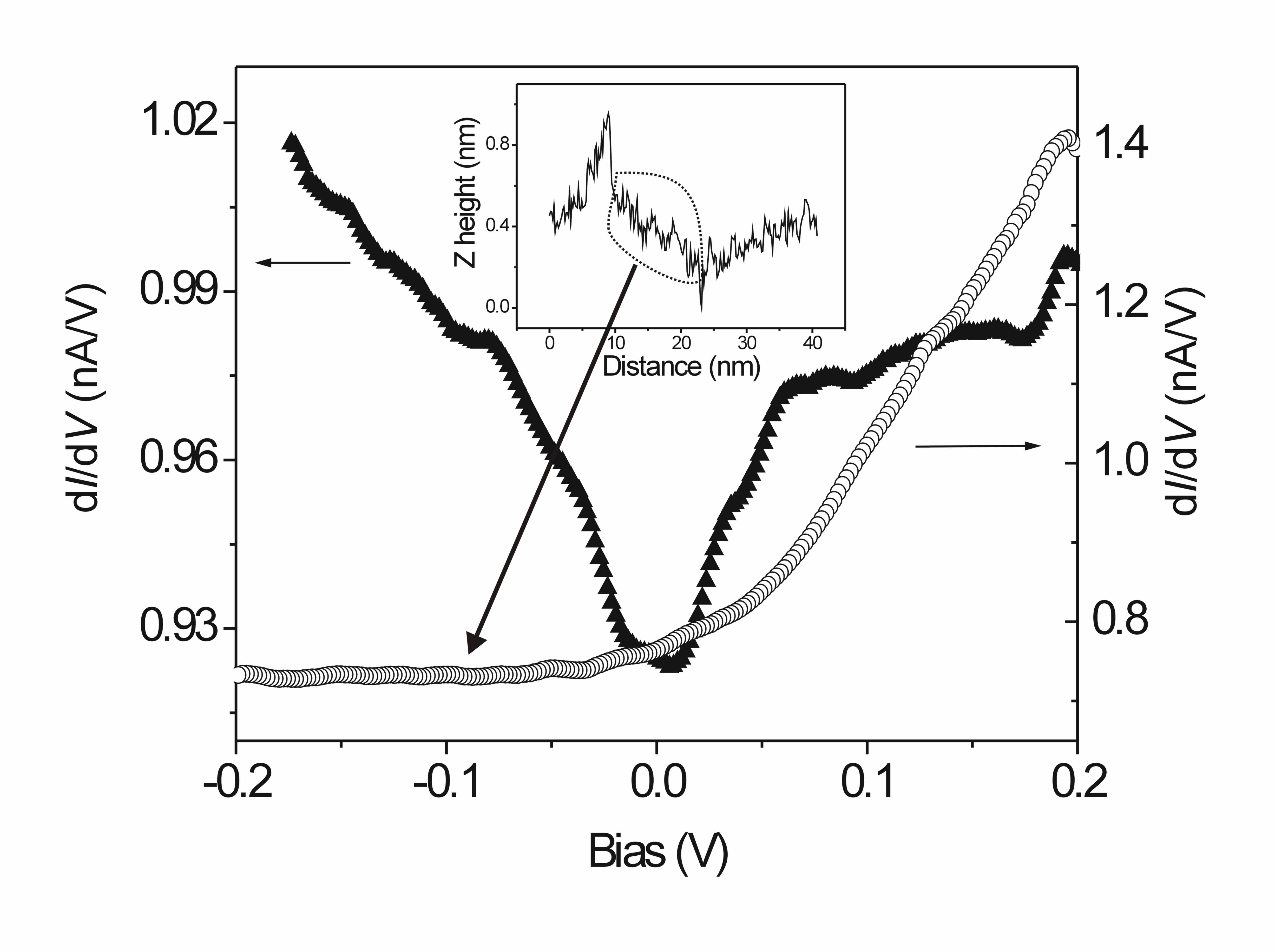
Spectroscopic data were taken at many different locations along and close to the twin boundaries. d/d curves obtained on the exposed part of the boundary are similar to the curves obtained on the entire area. These curves indicate a gap opening across the Fermi level. The curves are slightly asymmetric with the filled state gap edge higher than that of empty ones. The asymmetry of spectra representing superconducting areas has often been observed Anderson2006 ; Das2007 . In contrast, the d/d curves from the shoulder area are almost flat across the Fermi level. They are highly asymmetric with empty sample state conductivity higher than filled state ones. The underlying composition in this region is not known. It is, however, evident that the sample is locally nonsuperconducting. The width of the normal conducting region is of the order of 2. The absence of superconductivity in these regions could be due to a different oxygen content close to the twin boundary as compared to the entire superconducting matrix. The twin boundaries represent regions of high stress Maple2000 . We note here that this is the first direct observation of nanometer sized nonsuperconducting region along the twin boundaries of a sample in the superconducting state. So far the pinning effect of such nonsuperconducting regions is not clear. From the magnetization measurements, we have not observed any signature of pinning by these non superconducting regions. These regions might guide the vortex motion along the direction of the twin boundaries leading to channeling of vortices. The channeling effect was observed as a depression of the secondary peak in curves obtained for this sample Jirsa2007 .
In summary, we observed stripes of periodicity of a few hundreds of nm on the surface of NEG-123 single crystals. These stripes are most likely the growth steps and are present only on the sample surface. Stripes with periodicity of a few tens of nm were observed in the bulk. These bulk defects do not exhibit any preferred orientation in the crystal. Although no clear composition fluctuation could be detected across the stripes, we believe that the stripes are important for strong pinning similar to those in the melt-processed samples. Low temperature STM/STS data showed nonsuperconducting areas of nanometer-scale width aligned with the twin boundaries. The potential of these nonsuperconducting regions towards vortex pinning so far remains unclear.
References
- (1) M. Murakami, N. Sakai, T. Higuchi and S. I. Yoo, Supercond. Sci. Technol. 9, 1015 (1996).
- (2) G. Blatter, M. V. Feigelman, G. Geshkenbein, A. I. Larkin and V. Vinokur, Rev. Mod. Phys. 66, 1125 (1994).
- (3) N. Takezawa and K. Fukushima, Physica C290, 31 (1997).
- (4) J. Sosnowski, J. Phys. Conf. Ser. 43, 659 (2006).
- (5) M. Murakami, M. Morita, K. Doe and K. Miyamoto Jap. J. Appl. Phys. 28, 1189 (1989).
- (6) M. Muralidhar, N. Sakai, M. Nishiyama, M. Jirsa and M. Murakami, Appl. Phys. Lett. 82, 943 (2003).
- (7) A. Hu, I. Hirabayashi, M. Winter, M. R. Koblischka, U. Hartmann and H. Zhou, Appl. Phys. Lett. 86, 092505 (2005).
- (8) M. Muralidhar, N. Sakai, M. Jirsa, M. Murakami and N. Koshizuka, Supercond. Sci. Technol. 18, 092505 (2005).
- (9) M. R. Koblischka, M. Winter, A. Koblischka-Veneva, M. Muralidhar, F. Mücklich and U. Hartmann, Appl. Phys. Lett. 91 082508 (2007).
- (10) M. R. Koblischka, M. Winter, A. Hu., M. Murakami and U. Hartmann, Jpn. J. Appl. Phys. 45, 2259 (2006).
- (11) D. X. Chen and R. B. Goldfarb, J. Appl. Phys. 66, 2489 (1989).
- (12) M. Jirsa et al., Mat. Sc. Eng. B (submitted).
- (13) R. W. McCallum, M. J. Kramer, K. W. Denis, M. Park, H. Wu, and R. Hofer, J. Electron. Mater. 24, 1931 (1995).
- (14) M. Muralidhar, N. Sakai, N. Chikumoto, M. Jirsa, T. Machi, N. Nishiyama, Y. Wu and M. Murakami, Phys. Rev. Lett. 89, 237001 (2002).
- (15) A. de Lozanne, Supercond. Sci. Technol. 12, R43 (1999).
- (16) H. A. Weber, Handbook Phys. Chem. Rare Earths, Elsevier Science, Vol. 31, 2001.
- (17) M. R. Koblischka, A Koblischka-Veneva, P. Das, T. Wolf, F. Mücklich and U. Hartmann, Microsc. Microanal. 13, 356 (2007).
- (18) A. Hu, M. Murakami and Z. Zhou, Appl. Phys. Lett. 83, 1788, 2003.
- (19) J. S. Kirkaldy, Phys. Rev. B 30, 6889 (1984).
- (20) H. Zhang, U. Memmert, R. Houbertz, and U. Hartmann, Rev. Sci. Inst. 72, 2613 (2001).
- (21) P. W. Anderson and N. P. Ong, J. Phys. Chem. Solids 67, 1 (2006).
- (22) P. Das, M. R. Koblischka and U. Hartmann, J. Phys. Conf. Ser. 61, 234 (2007).