Single-valley high-mobility (110) AlAs quantum wells with anisotropic mass
Abstract
We studied a doping series of (110)-oriented AlAs quantum wells (QWs) and observed transport evidence of single anisotropic-mass valley occupancy for the electrons in a 150 Å wide QW. Our calculations of strain and quantum confinement for these samples predict single anisotropic-mass valley occupancy for well widths greater than 53 Å. Below this, double-valley occupation is predicted such that the longitudinal mass axes are collinear. We observed mobility anisotropy in the electronic transport along the crystallographic directions in the ratio of 2.8, attributed to the mass anisotropy as well as anisotropic scattering of the electrons in the X-valley of AlAs.
pacs:
81.05.Ea, 61.72.uj, 73.61.Ey, 71.70.FkStrain and quantum confinement play an important role in tuning the valley degeneracy in indirect bandgap semiconductors.sun ; dhar Two dimensional electron systems (2DESs) shayegan ; dasgupta as well as one dimensional systems (1D) moser1 ; moser2 ; gunawan in AlAs have been previously studied and analyzed for (001)-oriented quantum wells (QWs), both of which have a reduced valley degeneracy from the bulk. The 2D systems are seen to have an isotropic mobility resulting from doubly degenerate valleys with orthogonally oriented anisotropic masses. But the other facets of growth, like the (110)-oriented QWs have not been extensively explored. The knowledge of the doping efficiency for this orientation is necessary to grow optimally doped cleaved-edge overgrown quantum wires moser1 ; moser2 and the valley degeneracy is expected to be different from (001)-oriented wells. In this paper, we present an experimental study of a doping series of double-sided-doped QWs grown in (110)-orientation and show experimental evidence of single-valley occupancy and an anisotropic electron mass for these QWs. This has been further complemented with effective mass calculations with finite barrier that take strain into account, which explain how for (110)-oriented AlAs QWs, single-valley occupation is expected for the square well width 53 Å. Also, we deduced the donor binding energy and the doping efficiency. Previously, anisotropic single-valley systems have only been investigated in piezo-strained (001) AlAs samples vaki ; padm . In contrast, the (110) AlAs samples investigated in this Letter are singly-degenerate as a result of the growth orientation, require no additional piezo sample preparation to reach single-valley occupancy, and tend to show higher mobilities than those reported in piezo-strained samples.
Bulk AlAs is an indirect band gap III-V semiconductor with three degenerate conduction band valleys at the X-points of the Brillouin zone edge. The mass of each valley is anisotropic, with heavy longitudinal and light transverse mass = 1.1 and = 0.2 , respectively shayegan ; gun2 ; gun3 . In a 2D-confined system, the number of degenerate X-points depends on the growth direction and the QW width due to a balance of strain and confinement effects. For (001)-oriented QWs studied elsewhere with 55 Å, a single X-valley is occupied whereas 55 Å yields doubly-degenerate occupied X-valleys in the QW.vandest
We determine in this work how (110) QW valley degeneracy should depend on well width. The energy of an electron in a valley with index (= or ) is
| (1) |
where is the in-plane kinetic energy, is the 2D in-plane momentum relative to the -valley minimum, is the ground confinement energy, and is the strain induced energy shift at the Brillouin zone edge at the X-point.
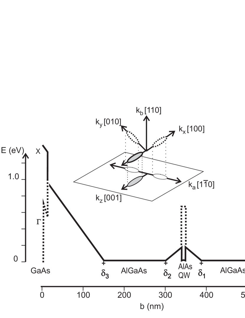
It is useful to introduce the cubic crystal axes and the growth axes ,moser1 related by the rotational transformation (Fig. 1)
| (2) |
Confinement energies are best determined by transforming the mass tensor to the growth-basis . In the crystal-basis , the mass tensor for the valley is diagonal with and for . Transforming to the growth-basis , the mass tensor becomes , so for the Xx-valley, for example with
| (3) |
with diagonal and off-diagonal mass terms. The diagonal mass will enter into the Schrödinger equation for the quantum well confinement energy.
Deformation potential energies are best determined by transforming the strain tensor to the crystal-basis . We assume that the AlAs QW ( Å) is strained relative to the GaAs substrate lattice ( Å) in agreement with previous publications. car ; vande ; vanKest For (110) biaxial strain, the perpendicular component can be deduced from the in-plane strain as , where is a constant that depends on the interface orientation and on the elastic constants of AlAs.vande ; kri In the growth-basis , is the growth direction, and the strain tensor is diagonal with , and . Transforming to the -basis, the strain tensor becomes with diagonal terms and .vande ; kri The energy at the valley minimum shifts from the unstrained case by an amount , where is defined in the crystal-basis , and the deformation potential for AlAs is eV. vande In our case, the single and double-degenerate X band edges are separated by 9 meV. Combining these new band edges with knowledge of the mass tensor, the Schrödinger equation can now be solved. All this information is automatically included in the publicly available simulation software nextnano3 (nextnano ) yielding a cross-over width = 53Å.
For , there is only a single occupied in-plane valley shown in shaded grey in Fig. 1 inset. The two higher-energy out-of-plane valleys are shown as dotted ellipsoids. For the role reverses, and these out-of-plane valleys become occupied. The projection of these valleys would be the white ellipsoids in the plane of the QW. Hence, the two valleys would have collinear longitudinal mass axes, in contrast to the (001) QW case where they are orthogonal.
Samples were grown on (110) GaAs substrates using molecular beam epitaxy. The structure of the samples is similar to the one discussed in Ref. 4 for the (001) facet and has been shown in Fig. 1. There is a 150 Å wide QW with three Si -doping layers. and separated from the QW by Al0.45Ga0.55As spacers provide electrons to the QW. These two -doping layers are doped equally with a Si density = = . The Si doping near the surface has higher density = and satisfies the surface states to pin the conduction band to the donor binding energy upon saturation. Various samples were grown with different doping indexed G through M.sample
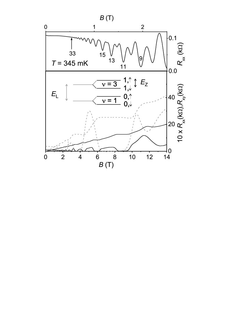
Indium contacts were annealed at 450 ∘C for 100 s. Two-point contact resistance was around 100 k at 300 K and around 40 k at 4.2 K. Samples were illuminated using a red LED of wavelength 635 nm. We performed post-illumination anneal at around 25 K (PIA) for these samples, described previously for (001) AlAs samples,dasgupta to obtain persistent photoconductivity. Typical longitudinal () and transverse () resistance variation with magnetic field at 330 mK in the dark and post-illumination for sample J in van der Pauw geometry is plotted in Fig. 2. The density of the samples in subsequent figures were deduced from such measurements.
The first evidence of single-valley occupancy for (110)-orientation comes from the periodicity at low magnetic field Shubnikov de Haas oscillations for the PIA data (Fig. 2 top). Due to the heavy cyclotron mass in AlAs, and large Lande g-factor of 2 (Ref. 21), the bare Zeeman energy is about half the bare cyclotron energy , so that in the absence of interactions, the case shown in the Fig. 2 inset. Exchange and correlation enhancement of is known to occur in AlAs quantum Hall systemspadm , and for the range , the Zeeman gap will be larger than the cyclotron gap and odd filling factor will dominate at low fields. As shown in the data of Fig. 2 top, the odd integers clearly dominate upwards and persist to filling factors as high as . In double-valley systems, by comparison, an additional factor of 2 appears in the filling factor due to valley degeneracy, and one observes prominent gaps in the series dasgupta .
The second evidence of single-valley occupancy comes from the anisotropic mobility in (110) QWs. We performed mobility measurements on a L-shaped Hall bar fabricated along the crystallographic axes [001] and [10]. The density in both arms is found to be the same, n = cm-2 and the mobilities in the two directions are = cm2/Vs and = cm2/Vs. The mobility anisotropy is consistent with anisotropic mass electrons conducting in a single-valley with the heavy mass oriented along the [001] direction and the light mass along the [10] direction, as expected in the single-valley degenerate system. We note that a naive Drude model of mobility is not sufficient since the mobility ratio is , whereas the inverse mass ratio is . There have been previous publications reporting similar non-Drude effects in anisotropic mass systemsbishop , and like these authors we propose that anisotropic scattering is responsible.tok
When the mobility is measured using van der Pauw geometry one obtains the mobility, ,vdp1 which is measured to be cm2/Vs. This can be related to the mobility in each crystallographic direction as .(Ref. 22) For our sample, the mobility was found to be cm2/Vs. This is within reasonable agreement to the van der Pauw mobility, which is within 20 of the average value. Comparing the (110) results here with Ref. 2 which has an identical structure on the (001) facet, we note approximately a factor of 6 reduction in van der Pauw mobility for the (110) grown quantum wells. These results would be discussed in more detail in an upcoming publication.dasgupta2
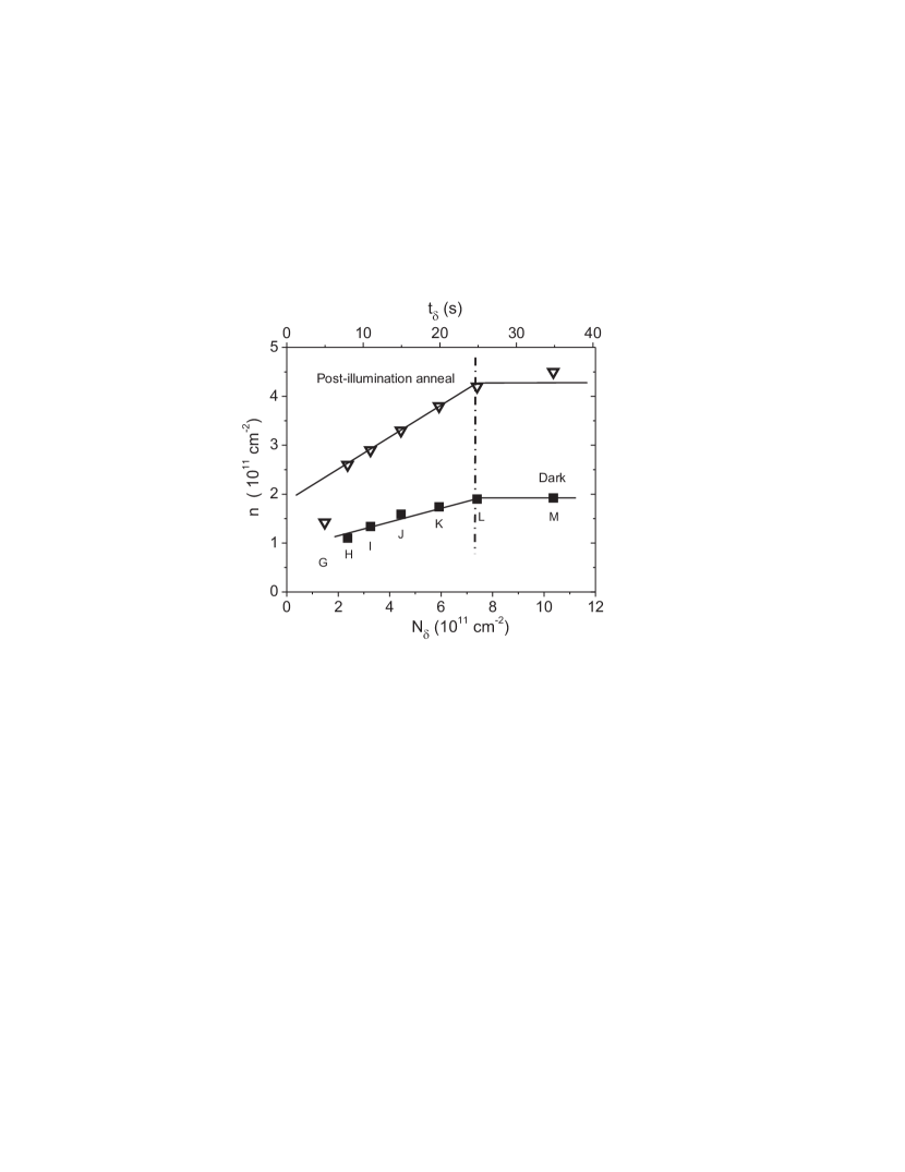
In Fig. 3 the 2DES density of the samples are plotted as a function of different Si doping concentrations deduced from the doping times, , with a calibrated Si flux of cm-2 s-1 for 11.4 A heater current. The dark electron density is seen to saturate at around = cm-2. Post-illumination anneal (PIA) density, plotted as triangles, is seen to saturate at about = cm-2. Sample L represents the optimally doped sample, since at higher doping approximiately the same saturation density is observed. Sample G works only post illumination. In the lowest density sample G, the post-illumination density drops abruptly, most likely indicating that the surface -doping layer is no longer in saturation. From the experimental dark density of , we deduce a donor binding energy of 66 meV and for , we deduce the post-illumination saturation binding energy of 0 meV using the same analysis presented in a previous publication.dasgupta The doping efficiency for the samples in the dark and post-illumination was calculated using the doping density at the saturation threshold shown with a vertical dashed line. We define from Ref. 4,
| (4) |
where is the doping efficiency. The factor of 2 in the denominator arises from the double-sided -doping layers, assuming that all surface states have been screened by the top -layer. Using this equation, we obtain the doping efficiency of in the dark and post-illumination anneal.
In summary, we have shown experimentally the occupation of the single X-valley by the 2DES in AlAs QWs in this (110)-orientation, which shows anisotropic mobility that can be partly attributed to the mass anisotropy. We have also presented results of a model calculation for the cross-over width in AlAs for (110)-orientation, which defines the QW width below which double-valleys are occupied and above which a single-valley is occupied. Furthermore, we have determined the binding energy of Si in -doped layers in Al0.45Ga0.55As in the dark and after illumination for the (110)-orientation and found them to be in the range of the values found for (001)-orientation. The doping efficiency for the Si -layers has been calculated to be in the dark and post-illumination anneal. These parameters will be instrumental in optimizing mobility in (110)-oriented AlAs QWs and cleaved-edge overgrowth structures.
This work was funded by BMBF nanoQUIT Project 01BM470 and the Nanosystems Initiative Munich (NIM).
References
- (1) Y. Sun, S. E. Thompson and T. Nishida. J. Appl. Phys. 101, 104503 (2007).
- (2) S. Dhar, E. Ungersböck, H. Kosina, T. Grasser and S. Selberherr. IEEE Trans. Nanotech. 6, 97 (2007).
- (3) M. Shayegan, E. P. De Poortere, O. Gunawan, Y. P. Shkolnikov, E. Tutuc and K. Vakili. Phys. Stat. Sol. B 243, 3629 (2006).
- (4) S. Dasgupta, C. Knaak, J. Moser, M. Bichler, S. F. Roth, A. Fontcuberta i Morral, G. Abstreiter and M. Grayson. Appl. Phys. Lett. 91, 142120 (2007).
- (5) J. Moser, T. Zibold, D. Schuh, M. Bichler, F. Ertl, G. Abstreiter, M. Grayson, S. Roddaro, V. Pellegrini. Appl. Phys. Lett. 87, 052101 (2005).
- (6) J. Moser, S. Roddaro, D. Schuh, M. Bichler, V. Pellegrini and M. Grayson. Phys. Rev. B 74, 193307 (2006).
- (7) O. Gunawan, B. Habib, E. P. De Poortere and M. Shayegan. Phys. Rev. B 74, 155436 (2006).
- (8) K. Vakili, Y. P. Shkolnikov, E. Tutuc, N. C. Bishop, E. P. De Poortere and M. Shayegan. Physica E 34, 89 (2006).
- (9) M. Padmanabhan, T. Gokmen, N. C. Bishop and M. Shayegan. arXiv:0807.1327v1
- (10) O. Gunawan, Y. P. Shkolnikov, E. P. De Poortere, E. Tutuc and M. Shayegan. Phys. Rev. Lett. 93, 246603 (2004).
- (11) O. Gunawan, E. P. De Poortere and M. Shayegan. Phys. Rev. B 75, 081304 (2007).
- (12) A. F. W. van de Stadt, P. M. Koenraad, J. A. A. J. Perenboom and J. H. Wolter. Surf. Sci. 361, 521 (1996).
- (13) C. G. Van de Walle. Phys. Rev. B 39(3), 1871 (1989).
- (14) J. A. Carlin, S. A. Ringel, R. N. Sacks and K. S. Yap. J. Vac. Sci. Technol. B 16, 1372 (1998).
- (15) H.W. van Kesteren, E.C. Cosman, P.Dawson, K.J. Moore and C.T. Foxon. Phys. Rev. B 39, 13426 (1989).
- (16) M. P. C. M. Krijn. Semicond. Sci. Tech. 6, 27 (1991).
- (17) www.nextnano.de: The tutorial for the 1D AlAs QW crossover width is publicly available for (001)- and (110)-oriented AlAs QWs. Simulations for the (001) facet under the same assumptions give Å, in excellent agreement with the experimentally observed cross-over of 55 Å.
- (18) G : 06-15-07.2, H : 06-15-07.1, I : 05-08-07.1, J : 05-08-07.2, K : 01-30-07.1, L : 01-05-07.2, M: 01-30-07.2
- (19) D. Bishop, R. C. Dynes, B. J. Lin and D. C. Tsui. Phys. Rev. B 30, 3539 (1984).
- (20) Y. Tokura. Phys. Rev. B 58, 7151 (1998).
- (21) L. J. van der Pauw. Philips Res. Repts. 13, 1 (1958).
- (22) L. J. van der Pauw. Philips Res. Repts. 16, 187 (1961).
- (23) S. Dasgupta, A. Fontcuberta i Morral, M. Bichler, G. Abstreiter and M. Grayson. Unpublished.