Optical probes of electron correlations in solids.
Abstract
Classically the interaction between light and matter is given by the Maxwell relations. These are briefly reviewed and will be used as a basis to discuss several techniques that are used in optical spectroscopy. We then discuss the quantum mechanical description of the optical conductivity based on the Kubo formalism. This is used as a basis to understand how strong correlation effects can be observed using optical techniques. We will discuss the use of sum rules in the interpretation of optical experiments. Finally, we describe the effect of including interactions between electronic and collective degrees of freedom on optical spectra.
pacs:
42.50.Ct, 71.36.+c, 78.20.-eI Introduction
We will discuss the physics of correlated electron systems from an experimental viewpoint, focussing on optical spectroscopy. The interaction of light and matter will be discussed first from a classical point of view, based on the Maxwell equations. This review will be the basis for a discussion of optical techniques that are most commonly used. We will then continue with a discussion of the quantum mechanical description of the interaction between light and matter, using the Kubo-formalism. We finally discuss the application of sum rules to correlated systems and what happens when interactions, like the electron-phonon interaction, become important. The first part of our review is not meant to be complete. Readers with interest for further details are referred to references (Wooten, ) and (Dressel, ). In the following all fields, currents, charge densities etc. are implied to be position and time dependent if not written explicitly. Bold quantities imply vectors or matrices.
II Electromagnetism and Matter
II.1 Maxwell’s equations
We start this review with the microscopic Maxwell equations,
| (1) | |||||
| (2) | |||||
| (3) | |||||
| (4) |
Here e and b are the microscopic electric and magnetic fields respectively. is the total microscopic charge distribution and the total microscopic current distribution (i.e. due to internal and external sources). Note that these equations are written in the C.G.S. system of units. To convert them to S.I. units, simply replace by . The charge distribution for a collection of point sources with charge can be written classically,
| (5) |
or quantum mechanically as,
| (6) |
Equations (1-4) are not very practical to work with. As a first step we rewrite them in a more familiar form. To do this we average the fields, charge and current distributions over a volume ,
| (7) | |||
| (8) |
and similarly for and . This is a sensible procedure under the condition that where is the Bohr radius. Using these averaged distributions we arrive at the standard Maxwell equations in free space,
| (9) | |||||
| (10) | |||||
| (11) | |||||
| (12) |
In order to see how matter interacts with propagating electromagnetic waves we have to distinguish between induced and external sources. We write and . Both the induced and external charge and current distributions have to obey the continuity equations separately,
| (13) |
We can distinguish three different types of macroscopic internal sources,
| (14) |
The first term on the right hand side, , corresponds to the response of the free charges. The second term is the current due to changes in the polarization state of the system. Finally, we include a term representing a current due to magnetization. Note that this last term is purely transversal (the divergence of a rotation is always zero) and so is easy to distinguish from the other two terms. Since the induced free charge current due to photons is necessarily transversal, , we can use the continuity equations to show that the induced free charge density has to be zero and as a consequence that the total induced charge density
| (15) |
It is convenient to introduce new fields
| (16) | |||
| (17) |
so that using equations (14-17) in equations (9) and (12) we find,
| (18) | |||||
| (19) |
II.2 Linear Response Theory
In the spirit of linear response theory we assume that the response of polarization, magnetization or current are linear in the applied fields:
| (20) | |||
| (21) | |||
| (22) |
The electric and magnetic susceptibilities can be expressed in terms of a dielectric function and magnetic permittivity . The dielectric function is a response function that connects the external field at position r and time with the field E at all other times and positions. So in general,
| (23) |
We will be mainly interested in the Fourier transform of however. It is an easy exercise to express the Maxwell equations in terms of q and which we leave to the reader. We can use these definitions to once again rewrite the Maxwell equations in the following form,
| (24) | |||||
| (25) | |||||
| (26) | |||||
| (27) |
We are now in a position to study the response of a solid to an externally applied field or light wave. For simplicity we assume that our solid is homogeneous so that and . We can describe light waves by plane waves, i.e.
| (28) | |||
| (29) |
Using (29) on the right hand side of Faraday’s equation (10) and rearranging we find,
| (30) |
If we now take the curl of this equation and use the fact that we can express M in terms of B as (see equations (17) and (21)),
| (31) |
we find that
| (32) | |||||
Note that in this equation we are left with only the transversal field since the curl of a curl is transverse. We give two further identities for completeness,
| (33) |
and,
| (34) |
Finally, we note that inside the solid . With this we have all the ingredients to express equation (19) in terms of E and J. We split this equation in transversal and longitudinal parts to find,
| (35) | |||||
| (36) |
We can define a new dielectric function with longitudinal and transverse components and write the previous equation in a more compact form,
| (37) |
This new dielectric function is now a complex quantity: . Using the last relation we can also define a complex conductivity and it is related to the dielectric function by,
| (38) |
The real part of is often called the reactive part and the imaginary part the dissipative part. The real and imaginary parts are also indicated with a subscript 1 and 2 instead of (’) and (”).
II.3 Kramers-Kronig relations
A fundamental principle in physics is the principle of causality: an effect cannot precede its cause. This principle provides us with a very useful relation between the real and imaginary parts of a response function like the optical conductivity as we now show. First we express the induced current due to an electric field in terms of a memory function,
| (39) |
The memory function has the property that . This is simply a restatement of the causality principle: we switch on a driving force at time so before that time there can be no current. We define the Fourier transform of in equation (39) as,
| (40) |
To do the integral we change to the complex frequency plane, . The exponential in Eq. (40) now splits in a complex and real part,
| (41) |
The second exponent in this integral is bounded in the upper half plane for and in the lower half plane for , so that we can evaluate the integral in the upper half plane since . We use the contour shown in figure 1.
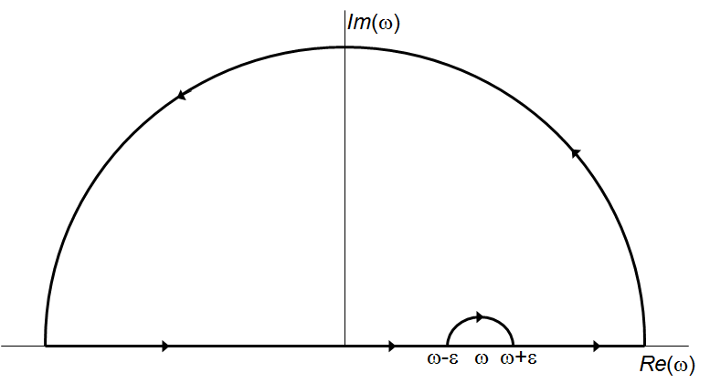
Since all poles occur on the real axis, the complete contour is zero,
| (42) |
The integral along the large semi circle is also zero. So we are left with,
| (43) |
The first two integrals give the principle value of the integral for ,
| (44) |
From which the Kramers-Kronig relations follow,
| (45) | |||||
| (46) |
Using we see that , which implies that and . These relations can be used to rewrite equations (45) and (46),
| (47) | |||||
| (48) |
The relations (45) and (46) between the real and imaginary parts of the optical conductivity are examples of the general relations between real and imaginary parts of causal response functions and they are referred to as Kramers-Kronig (KK) relations.
II.4 Polaritons
In this section we discuss the properties of electromagnetic waves propagating through solids. Such a wave is called a polariton. A polariton is a photon dressed up with the excitations that exist inside solids. For example one can have phonon-polaritons which are photons dressed up with phonons. Although the solutions of the Maxwell equations, i.e. the fields E and B, have the same form as before (Eq. (28) and (29)) they obey different dispersion relations as we will now see. As before we assume that and that . Taking the curl of Eq. (25) we obtain for the left-hand side,
| (49) |
where the T indicates that we are left with a purely transverse field. We then use Eq. (27) to work out the right-hand side of Eq. (25) and we obtain the wave equation,
| (50) |
From this wave equation we easily obtain the dispersion relation for polaritons travelling through a solid by substituting Eq. (28),
| (51) |
The dispersion relation for longitudinal waves can be found by observing that for longitudinal waves and hence the dispersion relation is simply,
| (52) |
The polariton solutions to Eq. (51) are of the form
| (53) |
with
| (54) |
We now define the refractive index,
| (55) |
In all cases considered here and . We also note that but it is possible to have . If the wave travelling through the solid gets attenuated,
| (56) |
The extinction of the wave occurs over a characteristic length scale called the skin depth,
| (57) |
Note that we can have if and so that the wave gets attenuated even though there is no absorption. In table 1 we indicate some limits of the skin depth.
| Insulator | ||||
| Metal | ||||
| Superconductor |
To illustrate some of the previous results we now have a look at the simplest model of a metal: the Drude-model. The optical conductivity in the Drude model is,
| (58) |
Often , the time in between scattering events, is written as a scattering rate . The plasma frequency is defined as . The dielectric function can now be written as,
| (59) |
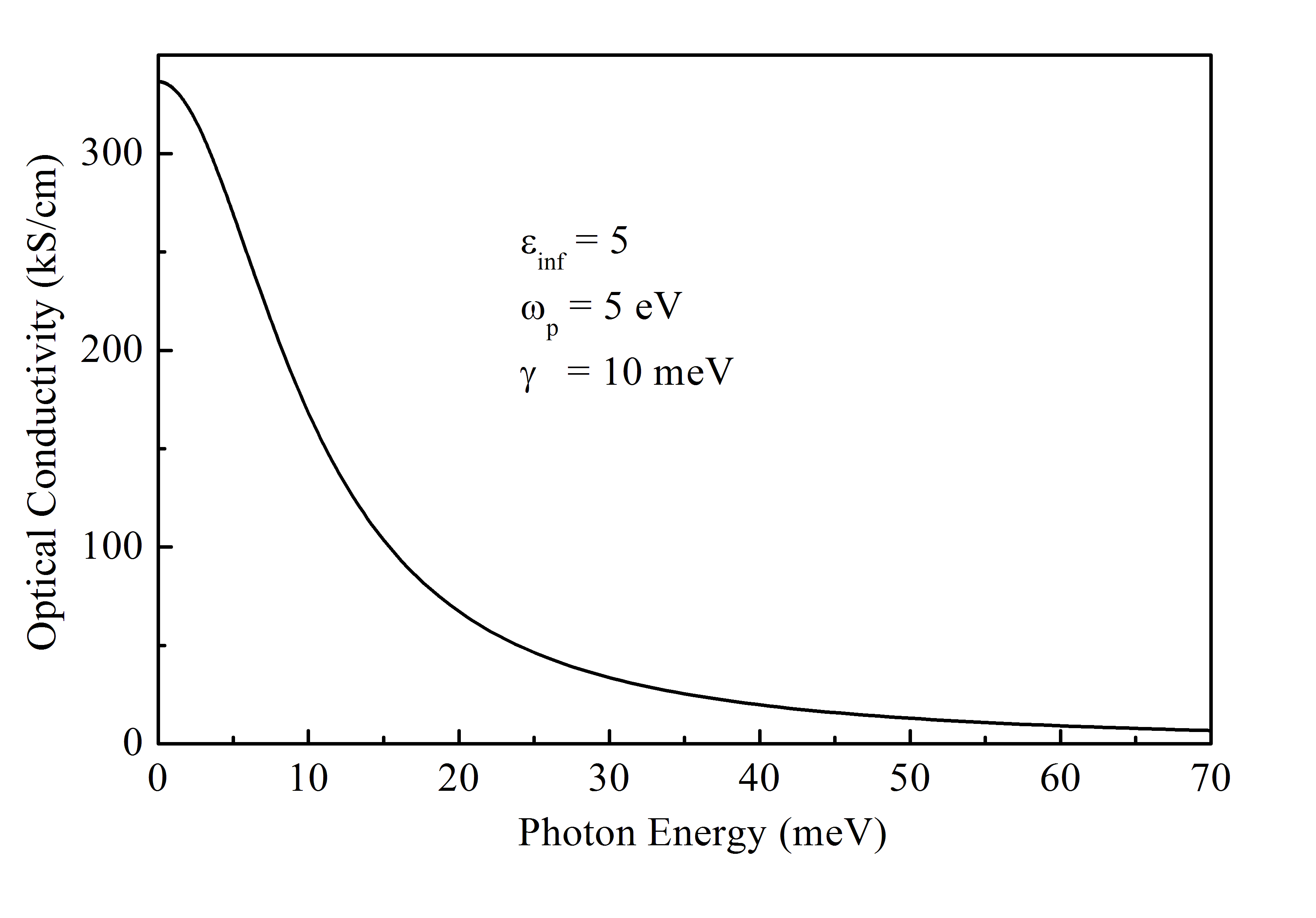
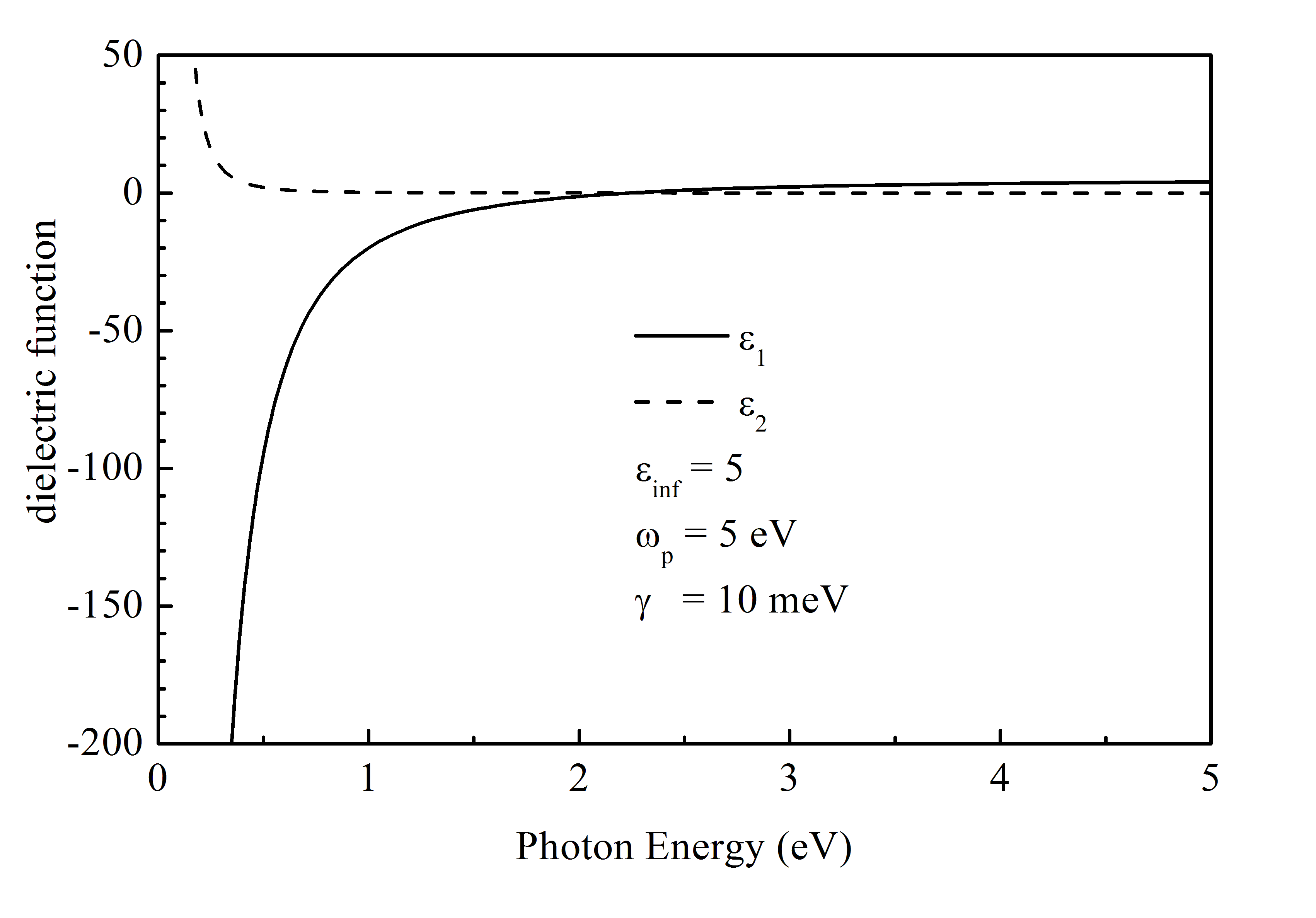
where for completeness we have included the contribution due to the bound charges, represented by a high energy contribution . Figure 3 shows the optical conductivity given by equation (58) for parameter values typical of a metal. Using the same parameters we can calculate the dielectric function given by equation (59). The results are shown in figure 3. We note that the real part of the dielectric function is negative for and positive for . The point where it crosses zero is called the screened plasma frequency (screened by interband transitions).
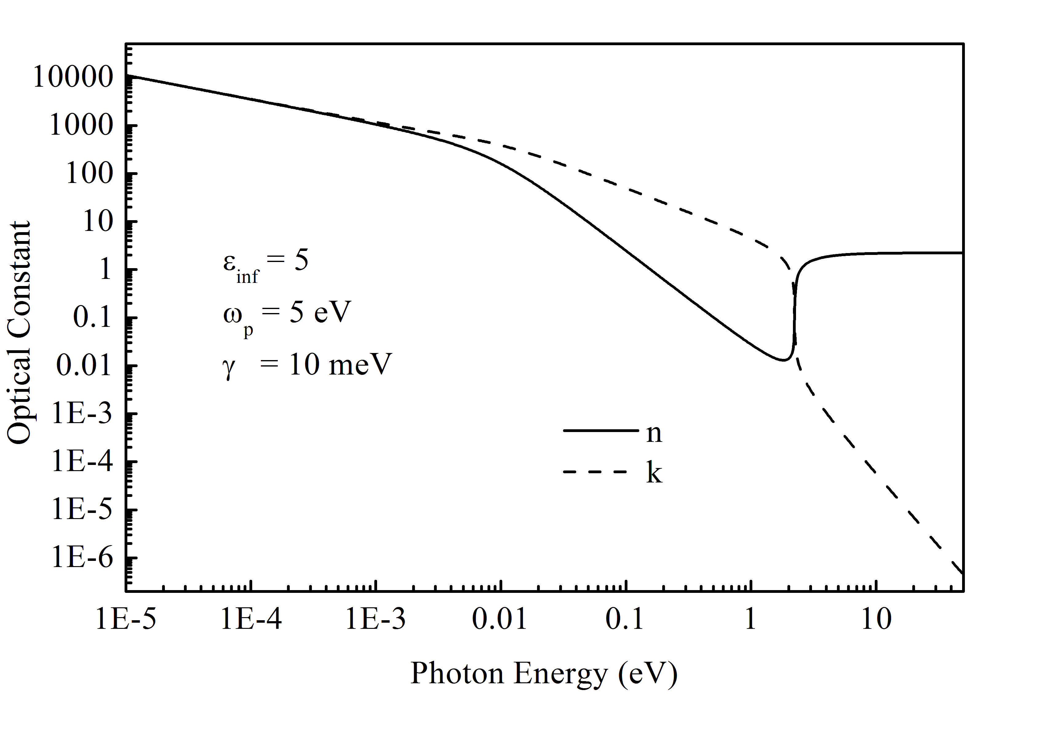
We can also easily calculate the optical constants,
| (60) |
The real and imaginary part are displayed in figure 5. We see that at the screened plasma frequency both and show a discontinuity.
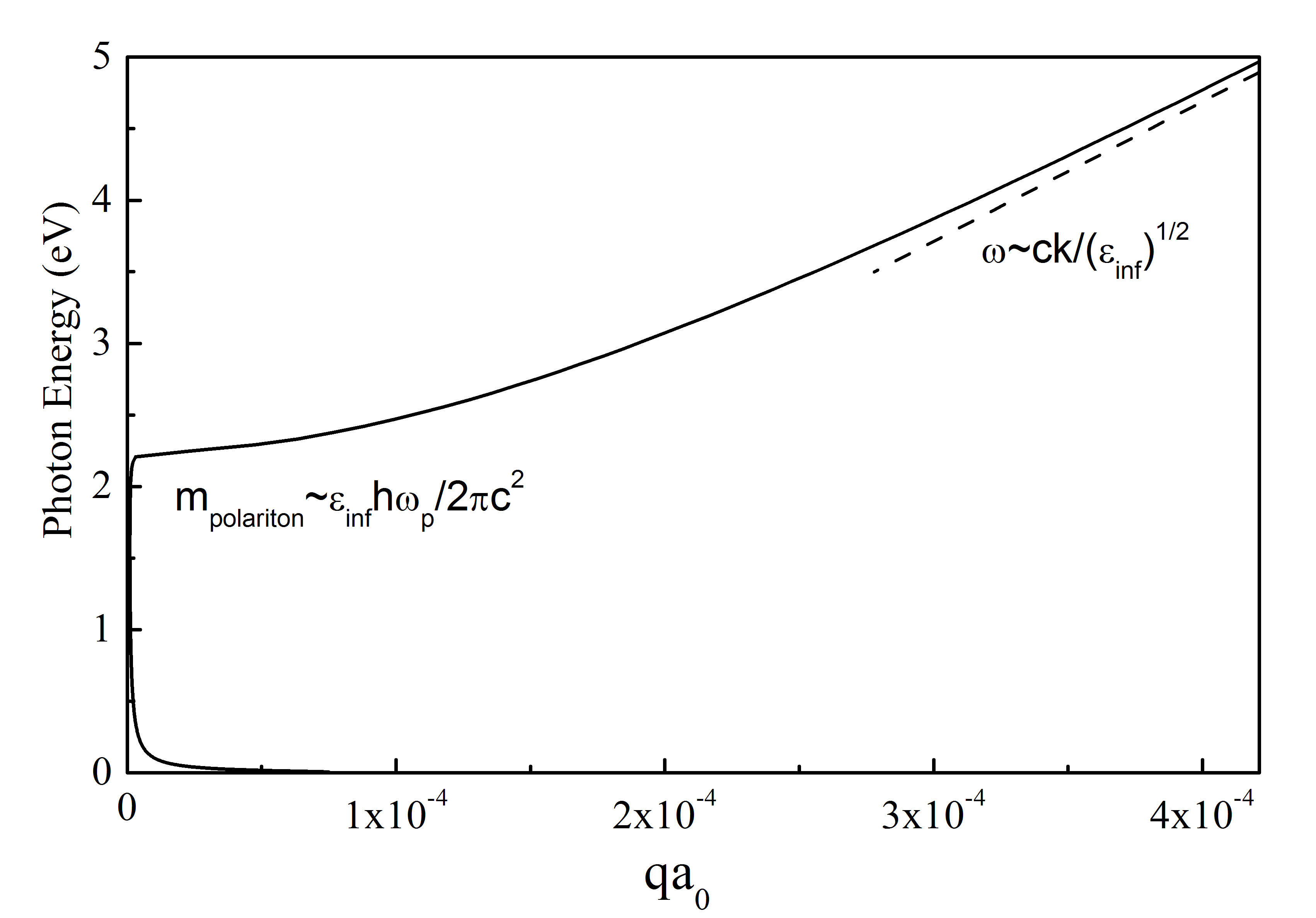
The polariton dispersion follows from equation (51). Here we assume that = 1 and frequency independent and use Eq. (59) to solve (51) for . The polariton dispersion consists of two branches the lowest one for 0 and one for .
Finally we show the skin depth in figure 6.
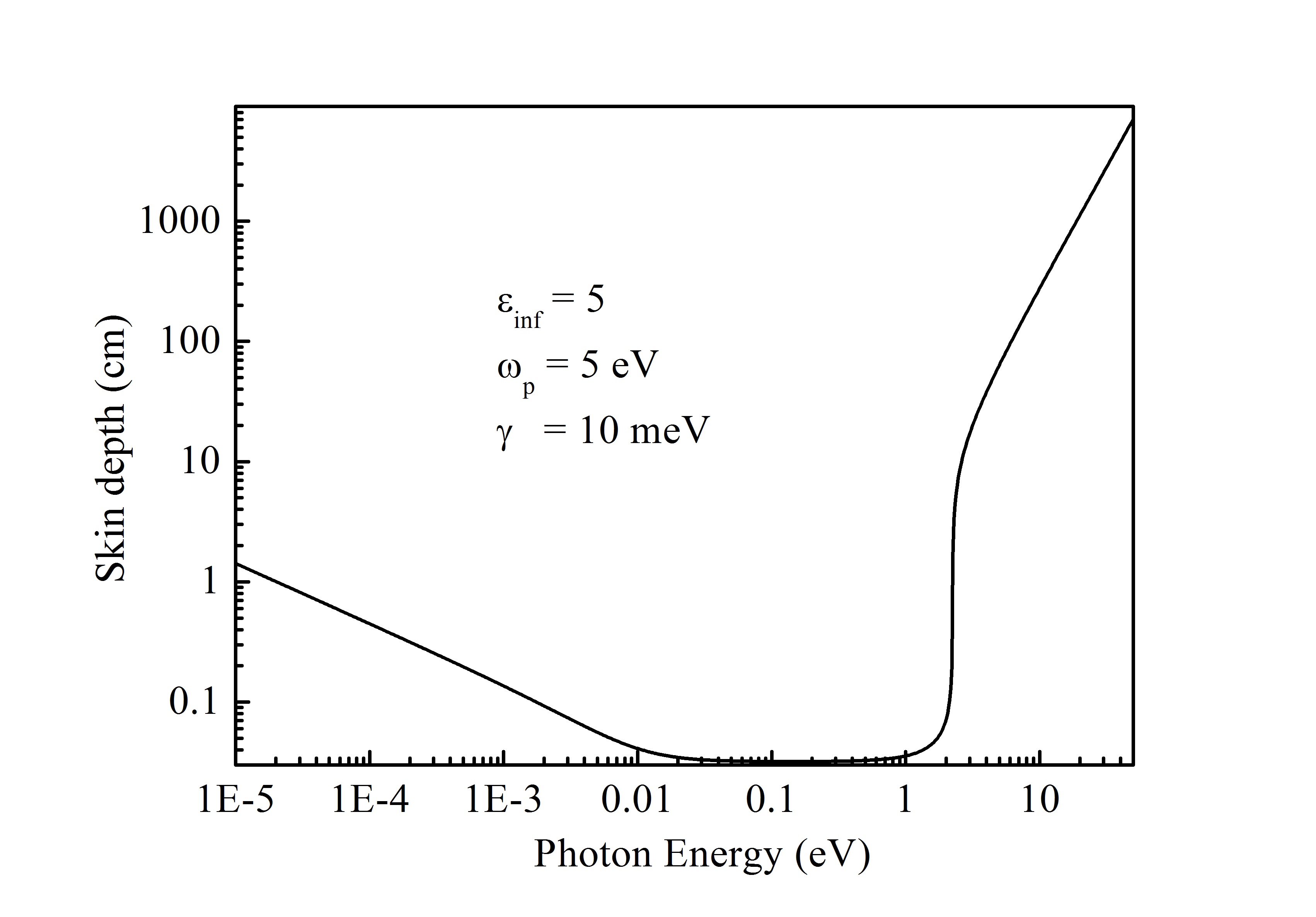
We see that for frequencies smaller than the scattering rate, , light waves can enter the material. This is called the classical skin effect. For frequencies larger than the screened plasma frequency the material becomes transparent again.
III Experimental Techniques
The goal of optical spectroscopy is to determine the complex dielectric function or equivalently the complex optical conductivity. Since electromagnetic waves have small momenta compared to the typical momenta of a solid, i.e. , we usually only probe the limit of the optical constants. In this limit,
| (61) | |||
| (62) |
In some cases we can directly obtain information on both real and imaginary components seperately, but more often we obtain information where the contributions are mixed. We then make use of some form the KK-relations to disentangle the two.
III.1 Reflection and Transmission at an interface
When we shine light on an interface between vacuum and a material, part of the light is reflected and another part is transmitted as in figure 7.
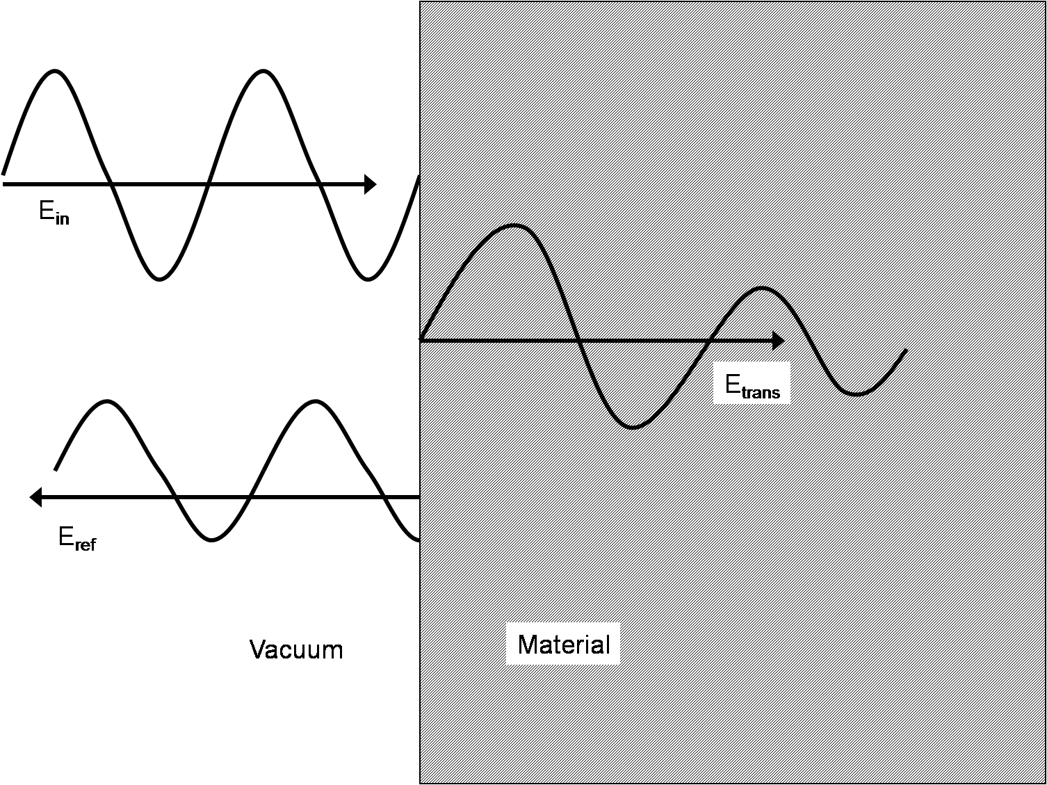
At the boundary the electromagnetic waves have to obey the following boundary conditions,
| (63) | |||
| (64) |
From these two equations it follows that the reflected magnetic field suffers a phase shift at the boundary,
| (65) |
Using equation (28) in equation (25) we obtain,
| (66) |
so that, using the dispersion relation (51),
| (67) |
From now on we set unless otherwise indicated. In that case . Combining this result with Eq. (65) we get,
| (68) |
Together with Eq. (63) we can now solve for and ,
| (69) | |||
| (70) |
The two quantities and are the complex reflectance and transmittance.
III.2 Reflectivity experiments
The real reflection coefficient which is measured in a reflection experiment is related to via
| (71) |
Note that in this experiment we obtain no information on the phase of . In these experiments the angle of incidence is as close to normal incidence as possible. To measure one first measures the reflected intensity from the sample under study. To normalize this intensity one then has to take a reference measurement. This can be done by replacing the sample with a mirror (i.e a piece of aluminum or gold) and again measure the reflected intensity, . The reflection coefficient is then . A better way is to evaporate a layer of gold or aluminum in-situ and measure the reflected intensity as a reference. This way one automatically corrects for surface imperfections and, if done properly, there are no errors due to different size and shape of the reflecting surface. To obtain the optical constants from such an experiment we have to make use of KK-relations. If we define, , then the logarithm of is
| (72) |
The phase in this expression is the unknown we want to determine. If we interpret as a response function we can use the same arguments as in the section on KK relations and calculate from,
| (73) |
which is just the same as the KK-relation for . The complex dielectric function is calculated from and using,
| (74) |
Although in principle exact, this technique is in practice only approximate. The reason is that we cannot measure from zero to infinite frequency. Most experiments probe a frequency range between a few meV and a few eV. To do the integral in Eq. (74) one then has to use extrapolations in the frequency ranges where no data is available. For metals the low frequency extrapolation which is most often used is the so-called Hagen-Rubens approximation,
| (75) |
For frequencies above the interband transitions one often uses an extrapolation that is proportional to .
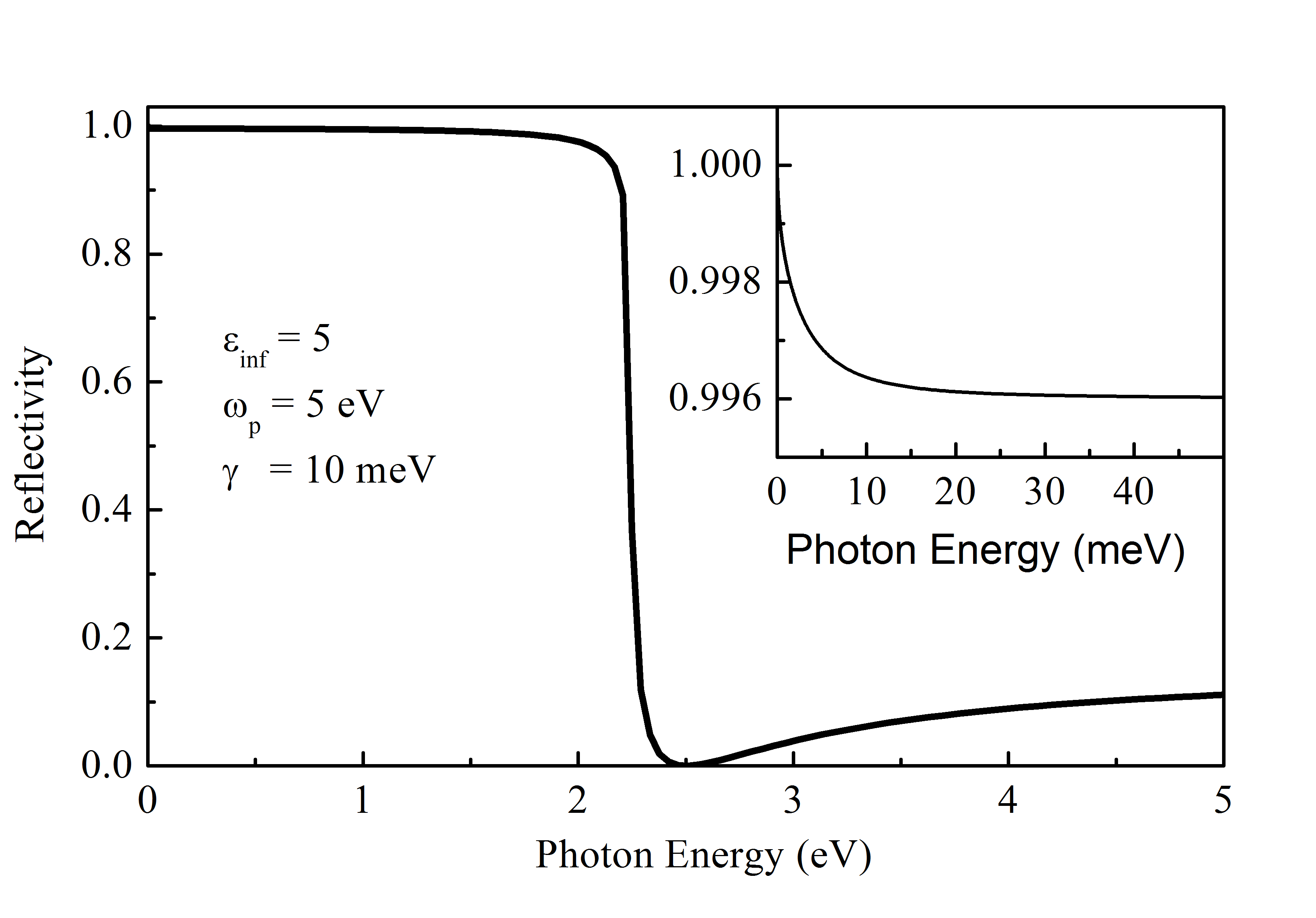
As an example of a possible experimental result we show in figure 8 the reflectivity calculated from the Drude model for the same parameters as in section on polaritons.
The reflectivity is close to one until just below the plasma frequency. At the zero crossing of the reflectivity has a minimum. The inset shows a blow up of the ”flat” region below 50 meV. Here one can clearly see the Hagen-Rubens behavior mentioned above. If the sample under investigation is anisotropic one has to use polarized light along one of the principle crystal axes to perform the experiment.
III.3 Grazing Incidence Experiments
A closely related technique is to measure reflectance under a grazing angle of incidence. Here one has to distinguish between experiments performed with different incoming polarizations as shown in figure 9.
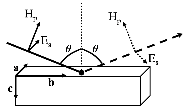
We distinguish between p-polarized light and s-polarized light. For p-polarization the electric field is parallel to the plane of incidence, whereas for s-polarization it is perpendicular to it (s stands for senkrecht). Since in principal the optical constants along the three crystal axes can be different, we use the labels , and for the optical constants as indicated in figure 9. For p-polarized light the complex reflectance is,
| (76) |
The angle in this equation is the angle relative to the surface normal under which the experiment is performed. For s-polarized light the complex reflectance is,
| (77) |
An example of such an experiment is shown in figure 10.
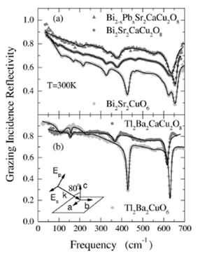
In this example the samples are from the bismuth based family of cuprates tsvetkov . They have a layered structure consisting of conducting copper-oxygen sheets, interspersed with insulating bismuth-oxygen layers. Since the bonding between layers is not very strong it is very difficult to obtain samples that are sufficiently thick along the insulating c-direction. The grazing incidence technique is used here to probe the optical constants of the c-axis without the need of a large ac-face surface area. A disadvantage in this particular experiment is that it is not possible to determine accurately the absolute value of the optical constants. It is possible however to determine the so-called loss function . The experiment is performed on the ab-plane of the sample using p-polarized light and we can simplify the expression for by using the fact that the and direction are almost isotropic. The resulting expression for is,
| (78) |
From this equation we can derive the following relation between the grazing incidence reflectivity and a pseudo loss-function dvdm ,
| (79) |
The function has maxima at the same position as the true loss-function. In this way information was gained on the phonon structure of the c-axis of this material.
III.4 Spectroscopic Ellipsometry
The third technique we introduce here is spectroscopic ellipsometry. This relatively new technique has two major advantages over the previous techniques. Firstly, the technique is self-normalizing meaning that no reference measurement has to be done and secondly, it provides directly both the real and imaginary parts of the dielectric function.
As with the grazing incidence technique we have to distinguish between s- and p-polarized light and label the crystal axes. Instead of measuring or independently, we now measure directly the amplitude and phase of the ratio . To see how this can be done we first describe the experimental setup. There are a number of different setups one can use and here we describe the simplest. This setup consists of a source followed by a polarizer. With this polarizer we can change the orientation of the polarization impinging on the sample.
The light reflected from the sample passes through another polarizer (called analyzer) and then hits the detector. Depending on the orientation of the first polarizer we can change the electric field strength of s- and p-polarized light according to,
| (80) | |||
| (81) |
From the expressions for and , (76) and (77), in the previous section it follows that,
| (83) |
Our task is now to invert this equation and express the optical constants in terms of measured quantities and instrument parameters. For an isotropic sample this can be done quite easily. We define the pseudodielectric function such that:
| (84) |
where we note that in an optically isotropic medium. This equation can be inverted to obtain ,
| (85) |
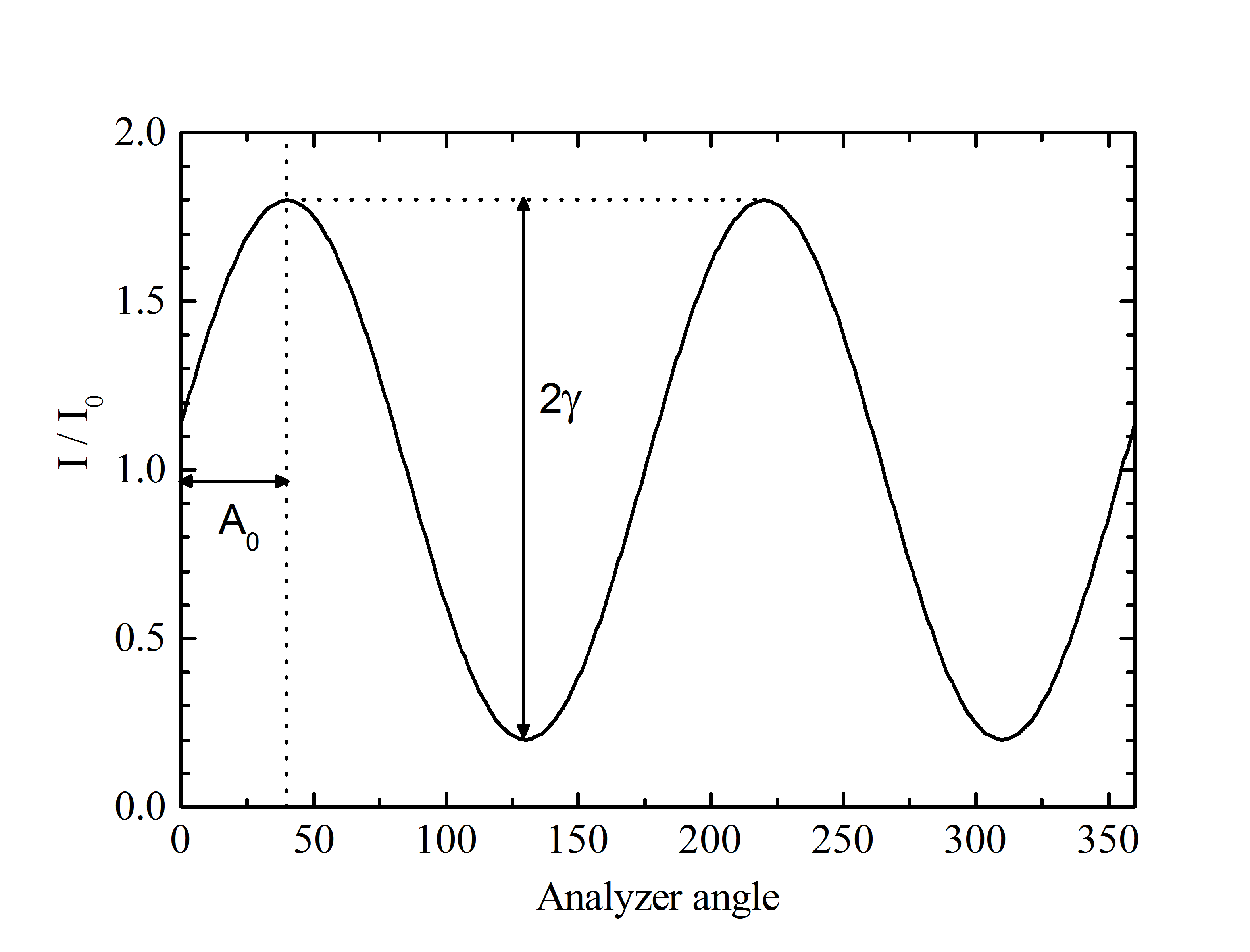
So all that is left to do is to express in terms of experimental parameters. The experiment is done in the following way: we fix the polarizer at some angle and then we record the intensity while rotating the analyzer 360 degrees. The result is shown in figure 11. We then measure the amplitude of the resulting sine wave, and the phase offset with respect to zero, (we assume here that for the polarizer and analyzer are aligned parallel to each other). With some goniometry and figure 11 we can show that,
| (86) |
and
| (87) |
Combining these two equations leads to,
| (88) |
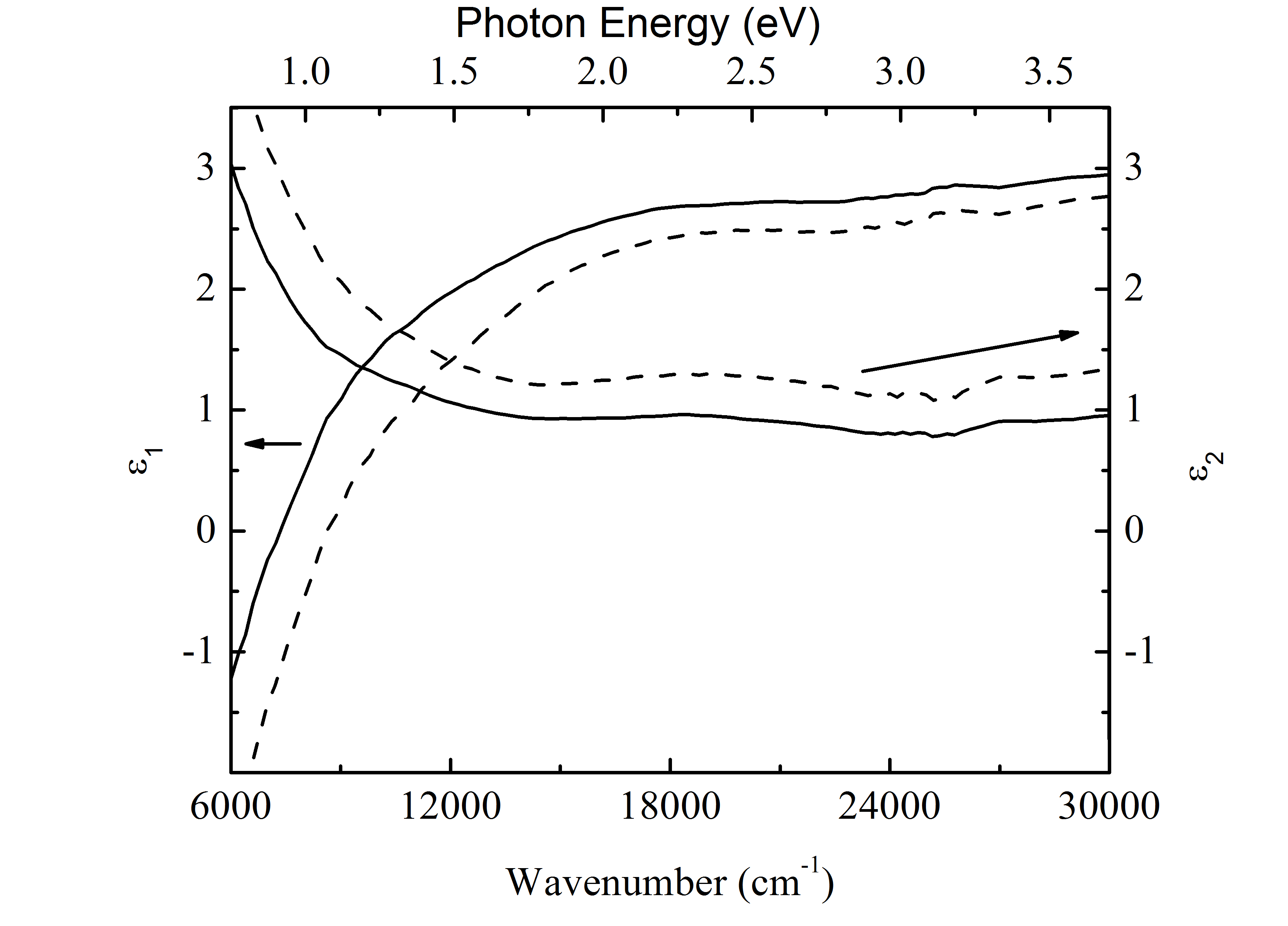
The combination of Eq. (88) with Eq. (85) is all we need to describe an ellipsometric experiment on an isotropic sample. For an anisotropic sample the problem is slightly more difficult. However, there exists a theorem due to Aspnes which states that the inversion of Eq. (83) results in Eq. (85) but now the dielectric function on the left-hand side is a so-called pseudo-dielectric function. This pseudo-dielectric function is mainly determined by the component parallel to the intersection of sample surface and plane of incidence (component along in figure 9), but still contains a small contribution of the two other components. If we perform three measurements, each along a different crystal axis, we can correct the pseudo dielectric functions and obtain the true dielectric functions. If the sample is isotropic along two directions, as is the case in high temperature superconductors for example, only two measurements are required. Figure 12 shows in dashed lines the pseudo dielectric function of HgBa2CuO4. In this case the and axes have the same optical constants. The c-axis dielectric function was determined from reflectivity measurements and subsequently used to correct the pseudo dielectric function measured by ellipsometry on the ab-plane. The true dielectric function after this correction is shown as the solid line.
III.5 Transmission Experiments
A technique complementary to the reflection techniques is transmission spectroscopy. This technique is, obviously, most suitable for transparent samples. In principle the technique can also be applied to metallic samples but this requires very thin samples or films. The reflection experiments discussed above are usually good methods to obtain accurate estimates of the real part of the optical conductivity. In contrast the transmission experiments discussed below are more sensitive to weak absorptions or, in other words to the imaginary part of the optical conductivity. Note that the simultaneous knowledge of reflection and transmission spectra allows one to directly determine the full complex dielectric function without any further approximations. Examples of weak absorptions which are better probed in a transmission experiment are multi-phonon or magnon absorptions. The equations for transmission experiments are slightly more difficult then those for the reflection experiments. These equations simplify if we do the experiment on a wedged sample as shown in figure 13.
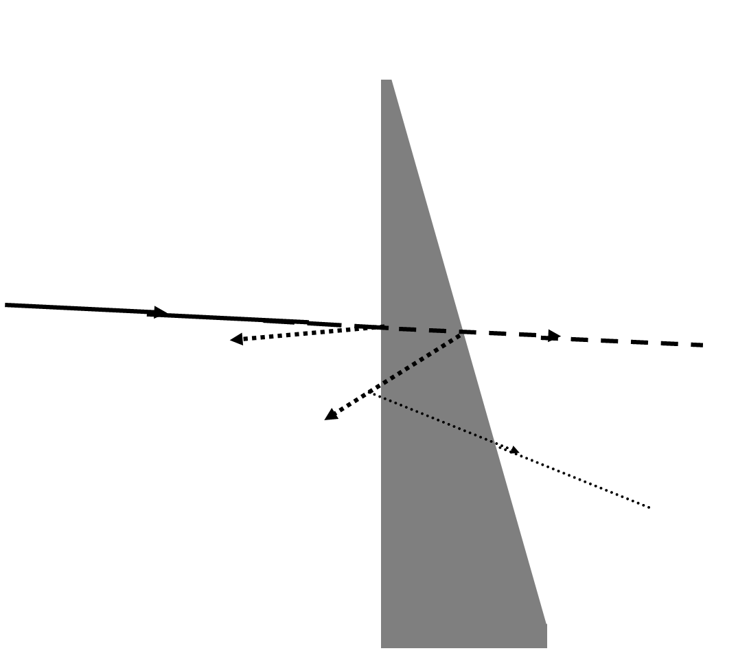
At the boundary between vacuum and the sample, part of the light is reflected and part transmitted. The part that is transmitted is given by,
| (89) |
Inside the wave propagates according to where,
| (90) |
At the next boundary again part of the beam is reflected back into the sample and part is transmitted. Now we can see the advantage of the wedged sample: the part of the light that is reflected propagates away at an angle and after another reflection the second transmitted ray is no longer parallel to and spatially separated from the first transmitted ray. This means that we only have to care about the first transmitted ray. The transmission coefficient at the boundary from sample to vacuum is given by,
| (91) |
so that the total transmission coefficient is,
| (92) |
Putting Eq.’s (89)-(92) together and taking the absolute value to calculate the transmission gives,
| (93) |
In most transmission experiments and the classical skindepth can be approximated by,
| (94) |
Moreover in these cases is often dispersion-less so that we can use the expression for to invert (93),
| (95) |
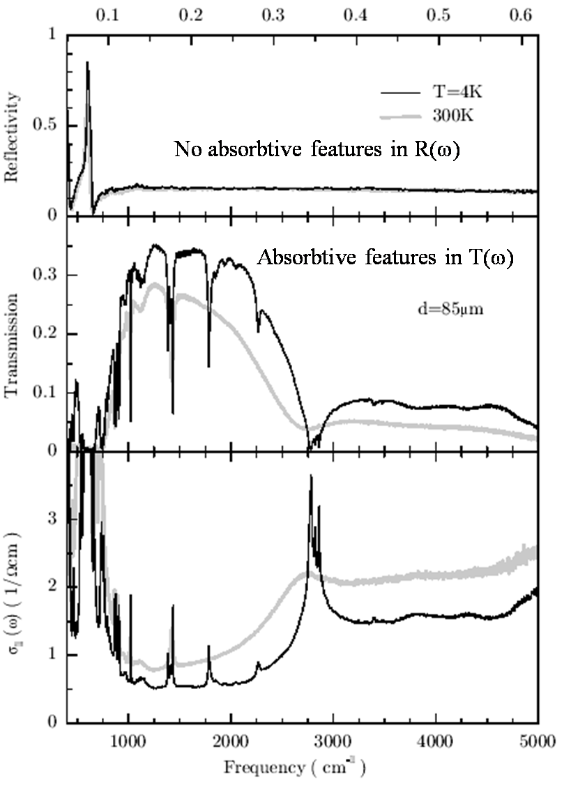
As an example of this technique we show in figure 14 a comparison between the reflectivity and transmission spectra of undoped YBa2Cu3O7 Grueninger . This material is an (Mott) insulator which is clearly visible from the reflectivity spectrum. The large structure at low energies is an optical phonon. At higher energy the reflectivity spectrum appears to be rather featureless. Focussing our attention on the transmission spectrum we see that it is almost zero in the phonon range but then above the phonon range a whole series of sharp dips shows up. The optical conductivity consists of a set of smaller peaks at energies between 100 meV and 300 meV which are due to multi-phonon absorptions whereas the larger peak just above 300 meV is due to a two magnon plus one phonon absorption (see also the section on spin interactions below).
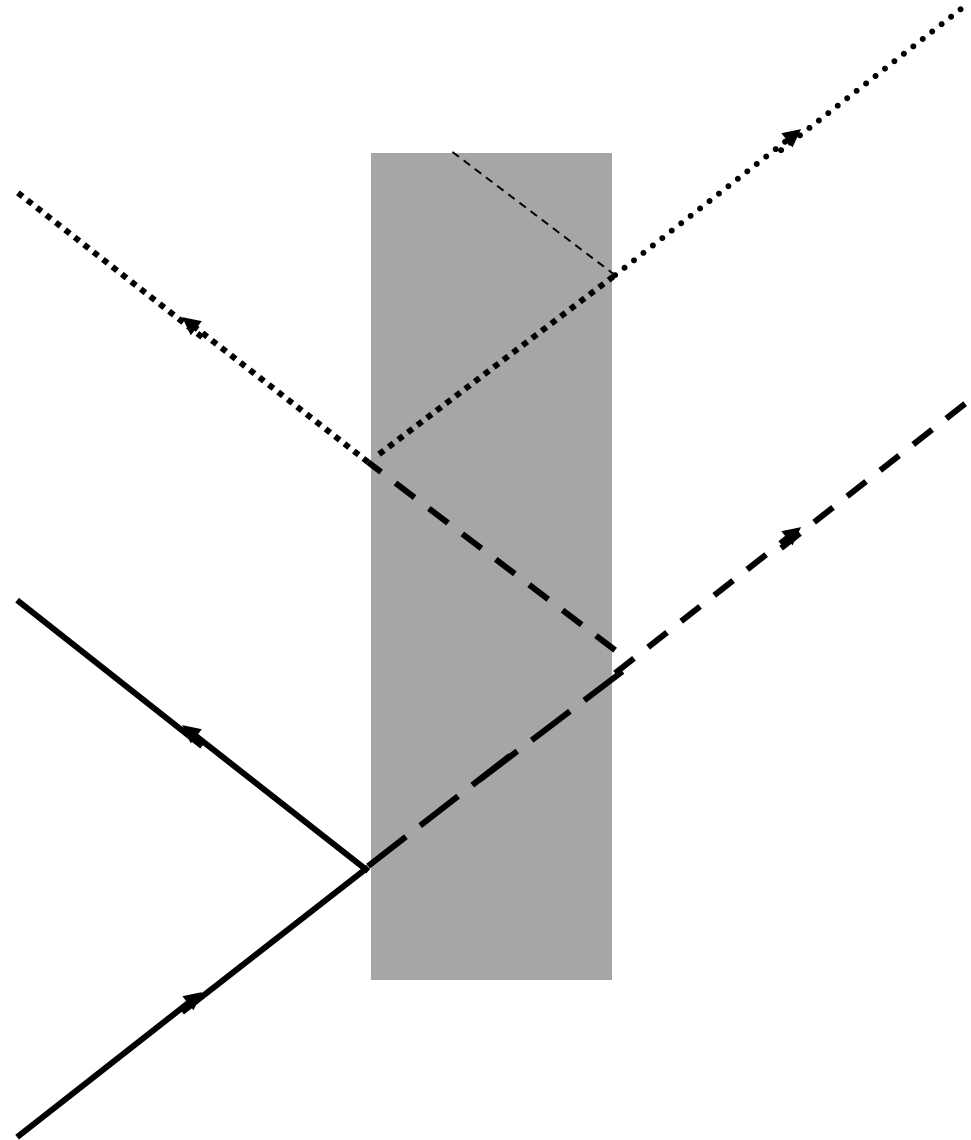
We can also do the experiment on a sample with two plan-parallel sides as depicted in figure 15. We can immediately realize that for a given thickness of the sample there will be interference effects between different transmitted rays for certain frequencies. These will cause oscillations in the transmission spectra which are called Fabry-Perot resonances. We now analyze the transmission coefficients for this experiment. The coefficient for the first ray is off course the same as in Eq. (92). The coefficients for the higher order rays are formed by multiplying on the right with a factor ,
| (96) |
followed by a factor . So the total transmission coefficient for the second transmitted ray is given by,
| (97) |
The coefficients and are given by Eq. (89) and (91). The coefficient for reflection on a boundary from sample to vacuum is given by,
| (98) |
It is easy to see that if we sum over all transmitted rays the total transmission coefficient is given by,
| (99) |
For thin films the phase factor and we can simplify this equation to,
| (100) |
and so,
| (101) |
More generally from Eq. (99) we obtain,
| (102) |
In the case that the sample under investigation has only weak absorptions, i.e. , this equation simplifies to,
| (103) |
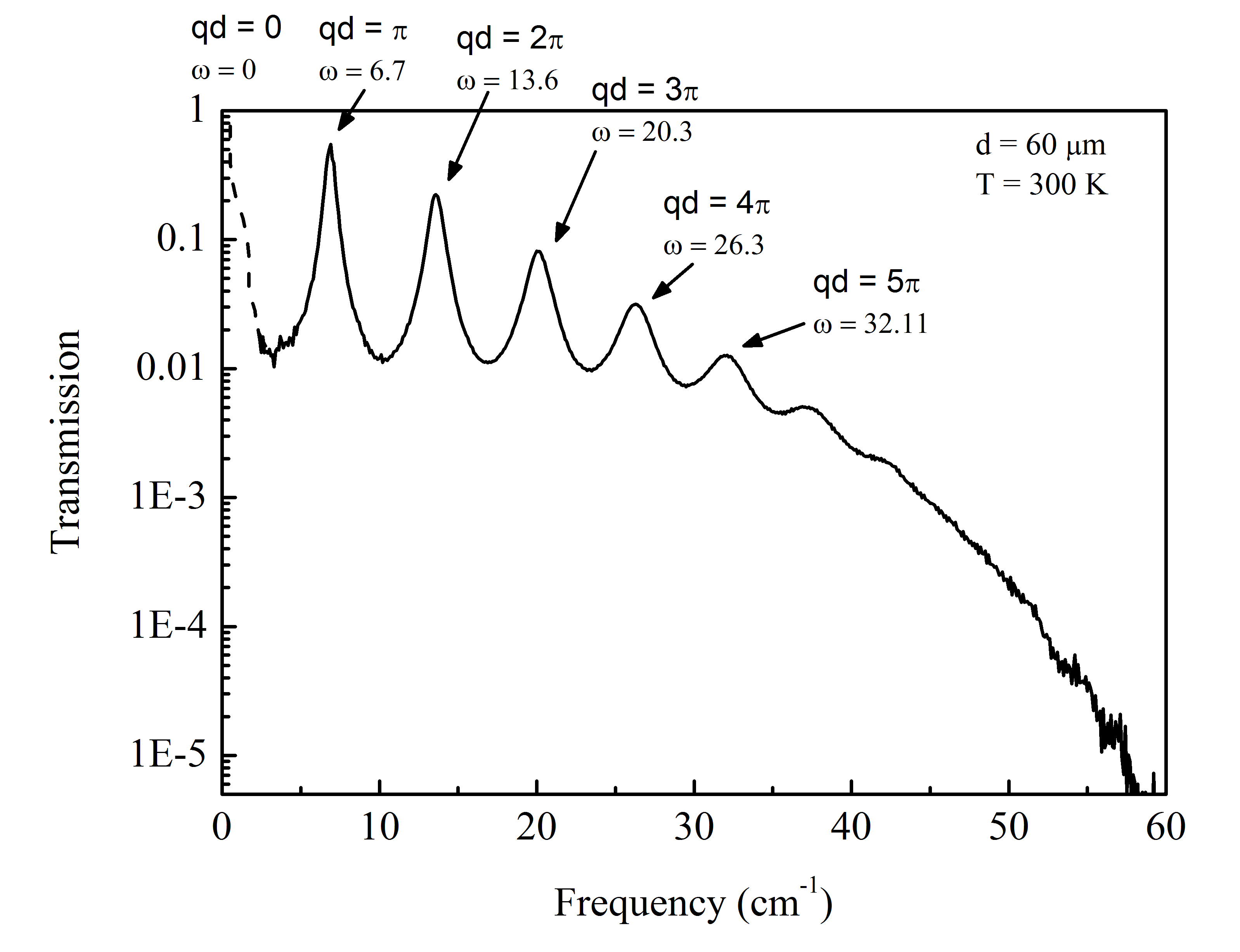
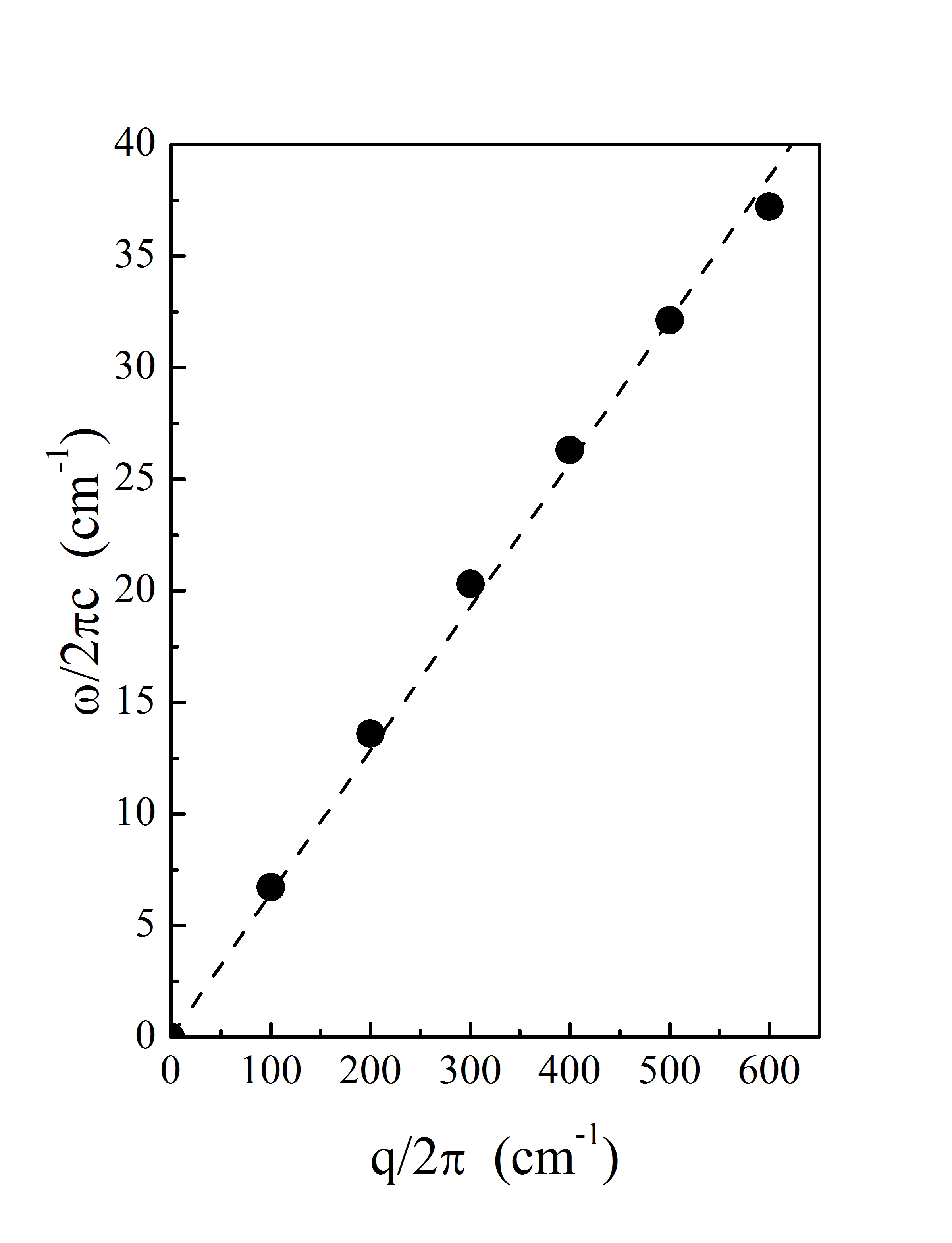
This equation gives us some insight to the occurrence of Fabry-Perot resonances: if with m=0,1,2,… the sinus is equal to zero and the transmission . In between these maxima the transmission has minima and . In reality the transmission will never reach 1 due to the fact that in which case our approximations are no longer valid. As an example we display in the left panel of figure 16 the transmission spectrum of SrTiO3 mechelen . This material is very close to being ferroelectric and as a result it has a very large dielectric constant. The non-sinusoidal shape of the peaks is due to this large dielectric constant. One can use the Fabry-Perot resonances to measure the polariton dispersion as we now show. Note that at each maximum in the transmission spectrum we know precisely the value of the argument of the sine function in Eq. (103).
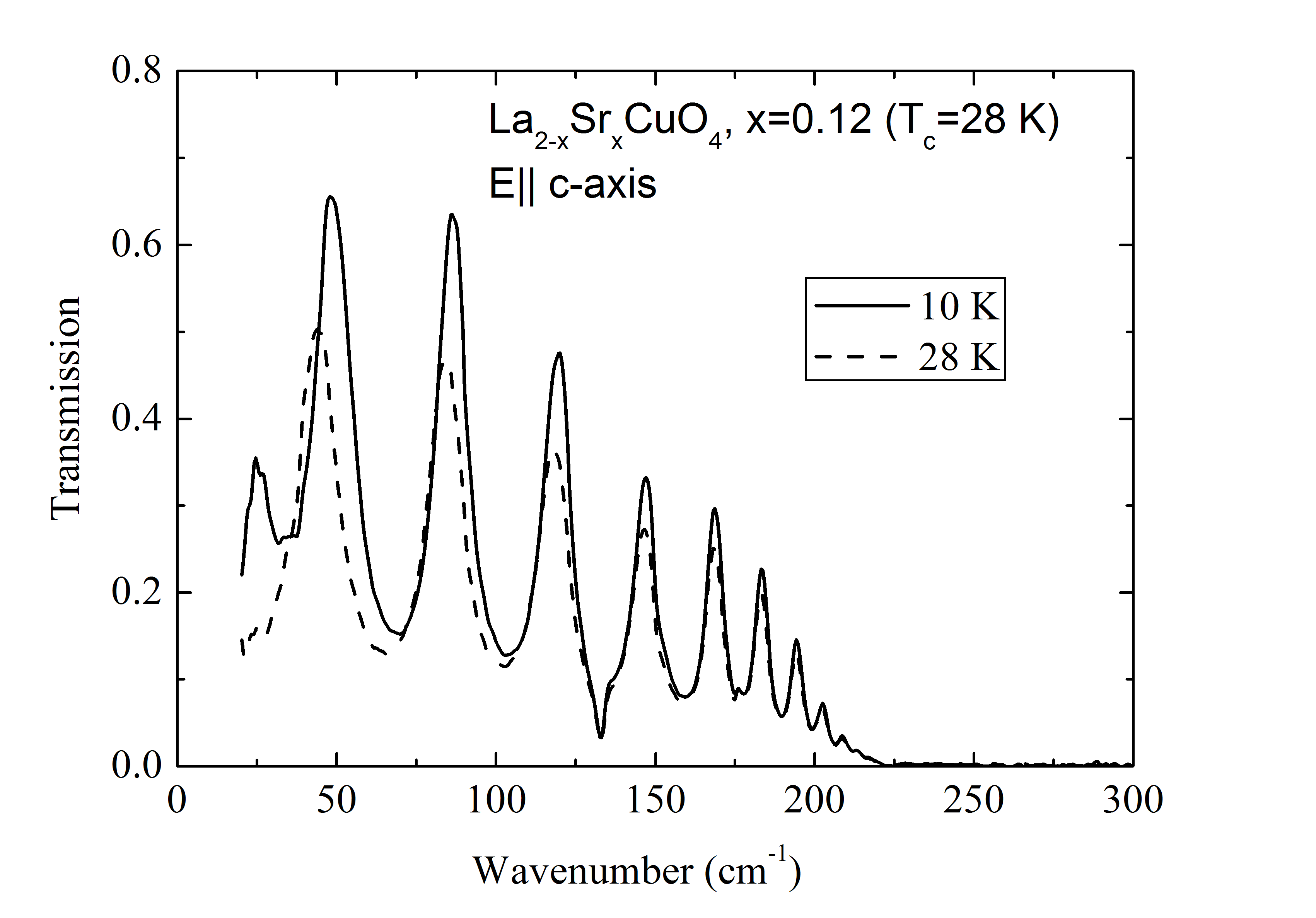
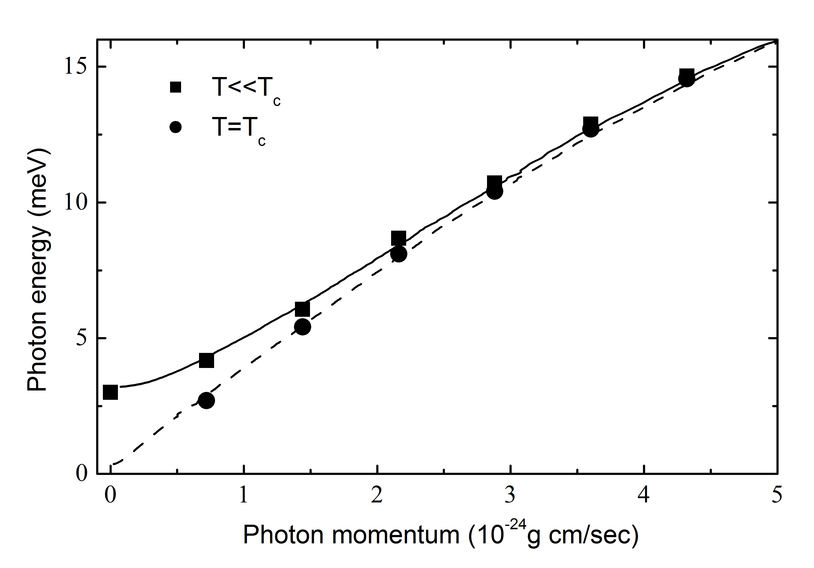
We can read off the value of from the graph and using Eq. (51) we can replace the argument in the sine function by so the momentum at a given maximum is,
| (104) |
So given the thickness of the sample we can make a plot of . The result for STO is shown in the right panel of figure 16. We see that the dispersion is linear, indicating that is dispersion-less in this range. The slope of the curve directly gives us . Another interesting application of this is to superconductors. In figure 17 we show the transmission spectrum of LSCO at a temperature slightly above Tc and far below kuzmenko . One can see that the position of the maxima has changed and this shows up in the polariton dispersion in an interesting way (see right panel figure 17). As in STO we see that in the normal state the dispersion is linear and extrapolates to zero. In the superconducting state the dispersion has acquired a dependence and no longer extrapolates to zero for . This is the result of the opening of the superconducting gap and it implies that the polaritons in the superconducting state have acquired a mass. This is an example of the Anderson-Higgs mechanismanderson , the same mechanism via which the Higgs-field gives a mass to the W and Z bosons in elementary particle physics. In the superconductor the order parameter plays the role of the Higgs-field and the spontaneously broken symmetry is that of the U(1) gauge symmetry.
III.6 TeraHertz time-domain spectroscopy
This relatively new technique is the last we will discuss here.
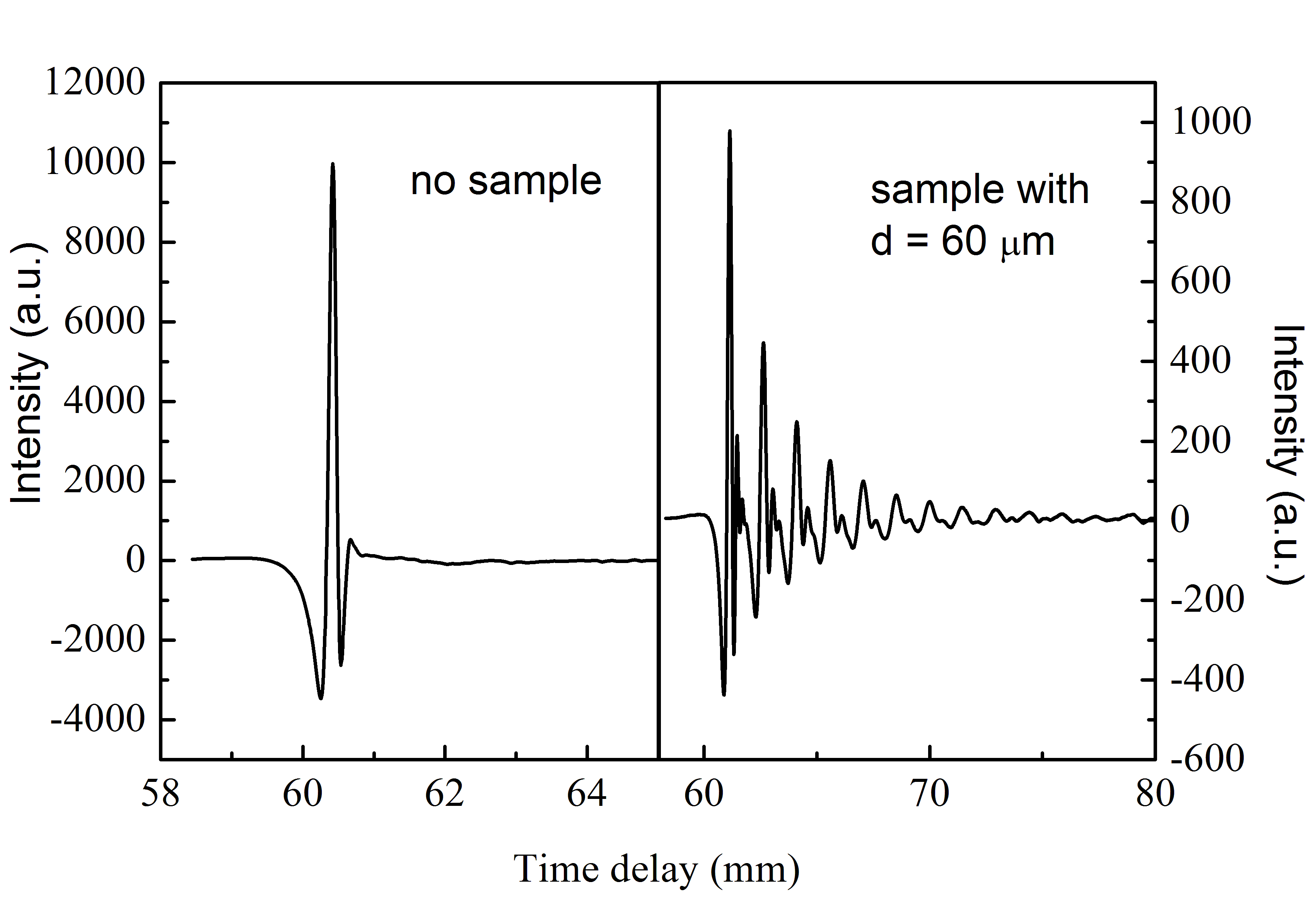
This technique uses a powerful laser pulse and records the detector output as a function of time, more often expressed in an optical delay distance. The result for an experiment in vacuum is shown in figure 18 on the left. If we now insert a sample that is transparent to terahertz radiation in the path of the beam we expect that due to the different optical path length in the sample the pulse will arrive at a later time. In fact, if we use a sample with to plane parallel surfaces we expect a series of peaks due to multiple reflections in the sample (see right panel of figure 18. These peaks are just a different manifestation of the Fabry-Perot oscillations observed in transmission spectroscopy. By Fourier transforming this signal to the frequency domain and doing the same for the signal without sample we can again obtain the transmission spectrum. The frequency domain spectrum corresponding to the time domain spectra of figure 18 is shown in figure 16.
IV Quantum theory
We now move to the quantum theoretical description of the interaction of light and matter using the Kubo-formalism. So far we have been using a ”geometrical” or macroscopic view of this interaction, but in this section we will consider the effects of the absorption of photons by electrons. Consider for simplicity a metal. The electronic states of the system are described by a set of bands, some of which are fully occupied, some partially and the rest empty, figure 19.
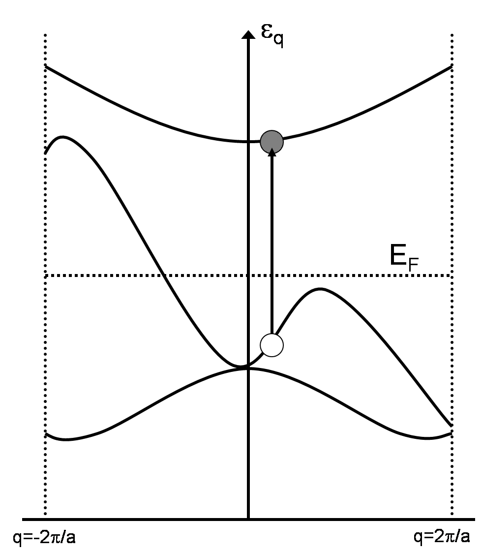
When photons interact with these band electrons they can be absorbed and in this process the electron is excited to a higher lying band leaving behind a hole. In this way we create electron-hole pairs and this (dipole) transition from a state to a state is characterized by an optical matrix element,
| (105) |
If the transition is from one band to another band we call the transition an interband transition and if the transition is within a band we call it a intraband transition. In figure 20 we show the optical conductivity of KCl. In this compound a strong onset is seen in the optical conductivity around 8.7 eV. This onset is due to the excitation of electrons from the occupied p-band related to the Cl- ions to the unoccupied s-band of the K+ ions. Since this particular transition involves moving charge from the chlorine atoms to the potassium atoms this type of excitation is called a charge transfer (CT) excitation zaanen .
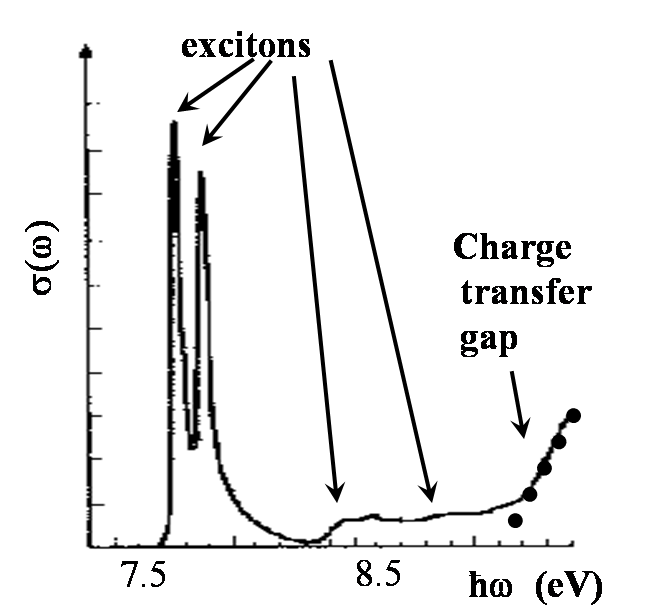
Another important feature in figure 20 are the strong peaks seen around 7.5 eV. Many theories often neglect so-called vertex corrections because these corrections cancel if the interactions between electrons are isotropic. However in real materials interactions are more often than not anisotropic and this means that these corrections have to be taken into account. The peaks seen in figure 20 are due to transitions from bound states of electron-hole pairs, called excitons, which arise due to the vertex corrections. Before we start our display of the Kubo-formalism we first introduce some notation. We introduce the field operators,
| (106) |
The density operator is given by,
| (107) |
The Fourier transform of is,
| (108) |
with
| (109) |
The velocity operator is defined as,
| (110) |
Finally, we note that the operators and satisfy,
| (111) |
IV.1 The Kubo-formalism
To calculate the optical conductivity from a microscopic starting point we have to add to the Hamiltonian of the system a term that describes the interaction with the electromagnetic field described by,
| (112) |
Note that we have chosen the transverse gauge which we will use throughout the rest of the chapter. The interaction Hamiltonian is given by,
| (113) |
and in the presence of an electromagnetic field we use the minimal coupling,
| (114) |
We now start by examining the current operator . It consists of two terms the first of which is called the diamagnetic term,
| (115) |
where in the last equality we have used Eq. (112). The second term is more difficult. It is given by,
| (116) |
We make here the approximation of using linear response theory: we expand the exponentials to first order in and then stop the series expansion. After some algebra we arrive at,
| (117) |
where we have defined,
| (118) |
The result we have obtained is for zero temperature but is easily generalized to finite if we use the grand canonical ensemble. Combining Eq. (115) and Eq. (117) we find for the optical conductivity,
| (119) |
where we have defined . The optical conductivity consists now of three contributions: the diamagnetic term followed by a contribution to positive frequencies and a contribution to negative frequencies. We note that in general is a tensor as indicated by the subscripts. We further note that the diamagnetic term does not give a real contribution to the conductivity. This term gives a -function contribution at zero frequency and this is exactly canceled by a delta function in the second part. This can be seen by using the fact that for every we have the following relationship,
| (120) |
So we can rewrite Eq. (119) as,
| (121) |
From here on we take the limit and define a generalized oscillator strength as,
| (122) |
With this definition we are lead to the Drude-Lorentz expansion of the optical conductivity,
| (123) |
IV.2 Sum Rules
Sum rules play an important role in optics. Using the equations of the previous section we derive the Thomas-Reich-Kuhn sum rule also known as the f-sum rule. The f-sum rule states that, apart from some constants, the area under is proportional to the number of electrons and inversely proportional to their mass. This can be shown as follows: integrating Eq. (123) we have,
| (124) |
Using the expression for , Eq. (122), and expression (120) we can rewrite the sum on the right hand side as,
| (125) |
So the f-sum rule states that,
| (126) |
as promised. This is the full universal sum rule. It is often rewritten as an integral over positive frequencies only and using the definition of the plasma frequency ,
| (127) |
as,
| (128) |
We can also define partial sum rules, i.e. sum rules where we integrate up to a certain frequency cutoff . In such a case the sum rule is not universal (this means for instance that the value of this sum rule can depend on temperature) and we can now define a plasma frequency that depends on the chosen cutoff frequency,
| (129) |
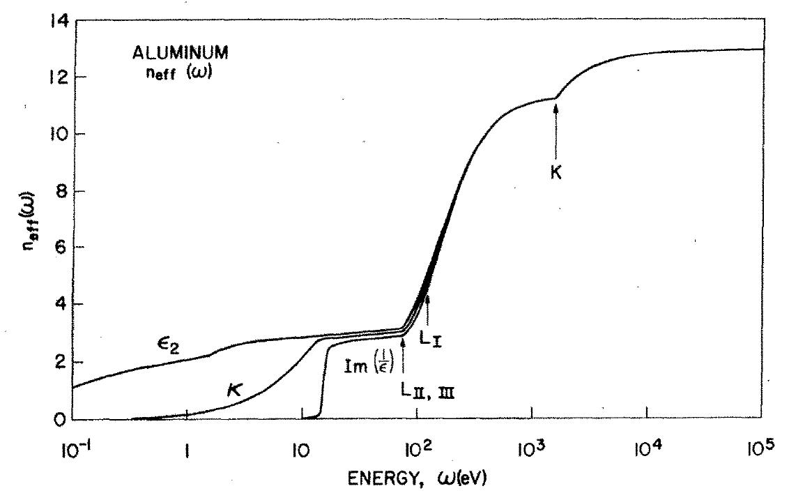
A nice example of the application of the partial sum rule is shown in figure 21. Here the partial sum rule is applied to the optical conductivity of aluminum smith . Here the effective number of carriers contributing to the sum rule is plotted as a function of . slowly increases to a value of roughly three around 50 eV. This means that as we increase the cutoff from zero to 50 eV we are slowly integrating over the intraband transitions and when we reach a value of 50 eV we have integrated over all transitions involving the three valence electrons. For higher energies the interband transitions start to contribute with a sharp onset near 80 eV. Finally at 104 eV the sum rule saturates at 13 electrons, the total number of electrons of aluminum.
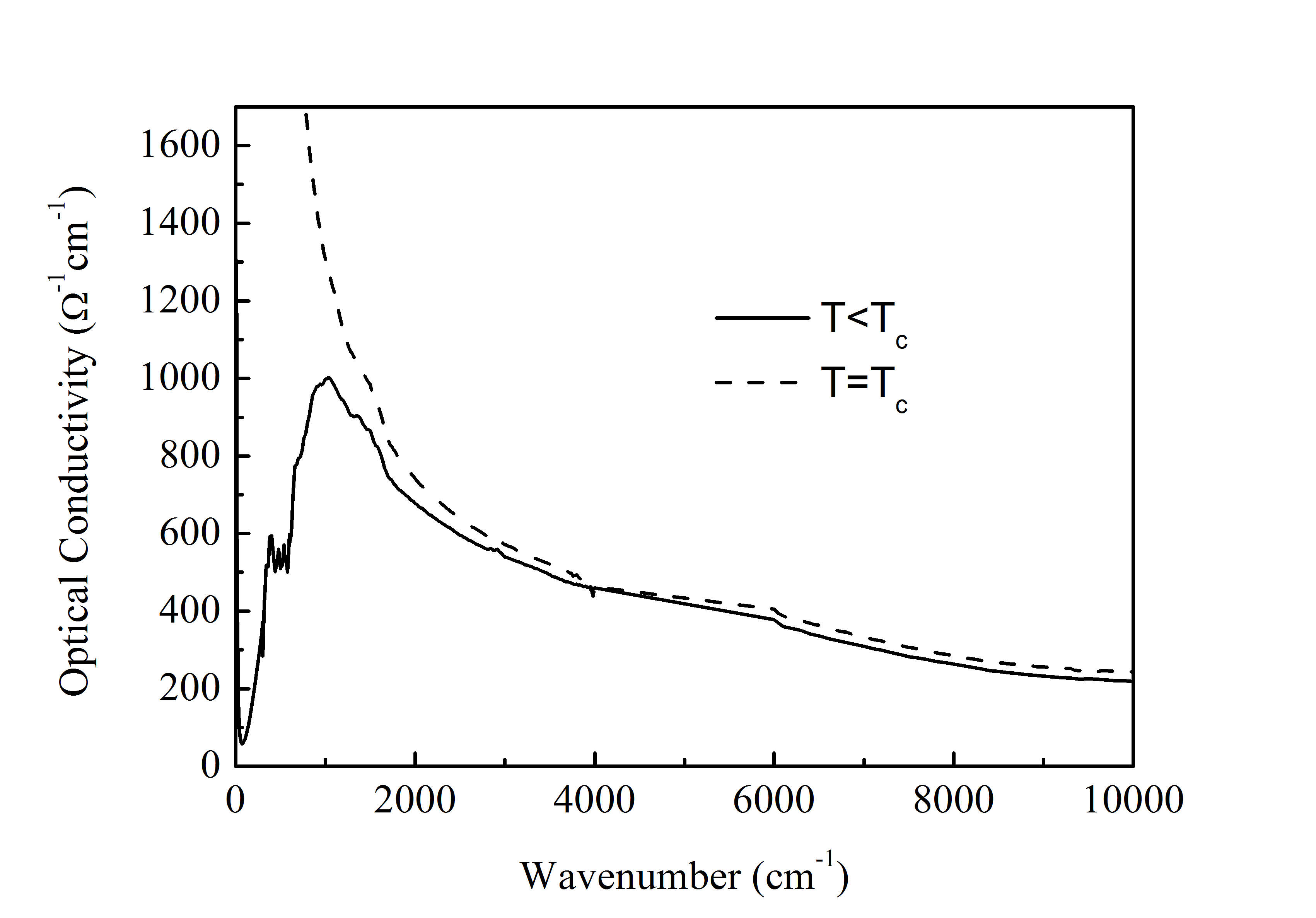
Another application of sum rules can be found in superconductors. In a superconductor the electrons form a superfluid condensate. This condensate shows up in the optical conductivity as a delta function at zero frequency (it contributes a diamagnetic term as in Eq. (119)). At the same time a gap opens up in low frequency part of the spectrum where the optical conductivity is (close to) zero, see figure 22. In the normal state the system is usually metallic and characterized by a Drude peak. In optical experiments we cannot measure the zero frequency response and so we cannot directly measure the spectral weight of the condensate. However, using sum rules we can estimate its spectral weight because the total spectral weight has to remain constant. This is summarized in the Ferrel-Glover-Tinkham (FGT) sum rule ferrel , which states that the difference in spectral weight between the optical conductivity in the superconducting and normal state is precisely the spectral weight of the condensate,
| (130) |
Note that we integrate here from 0+.
There also exist sum rules for mixtures of different types of particles,
| (131) |
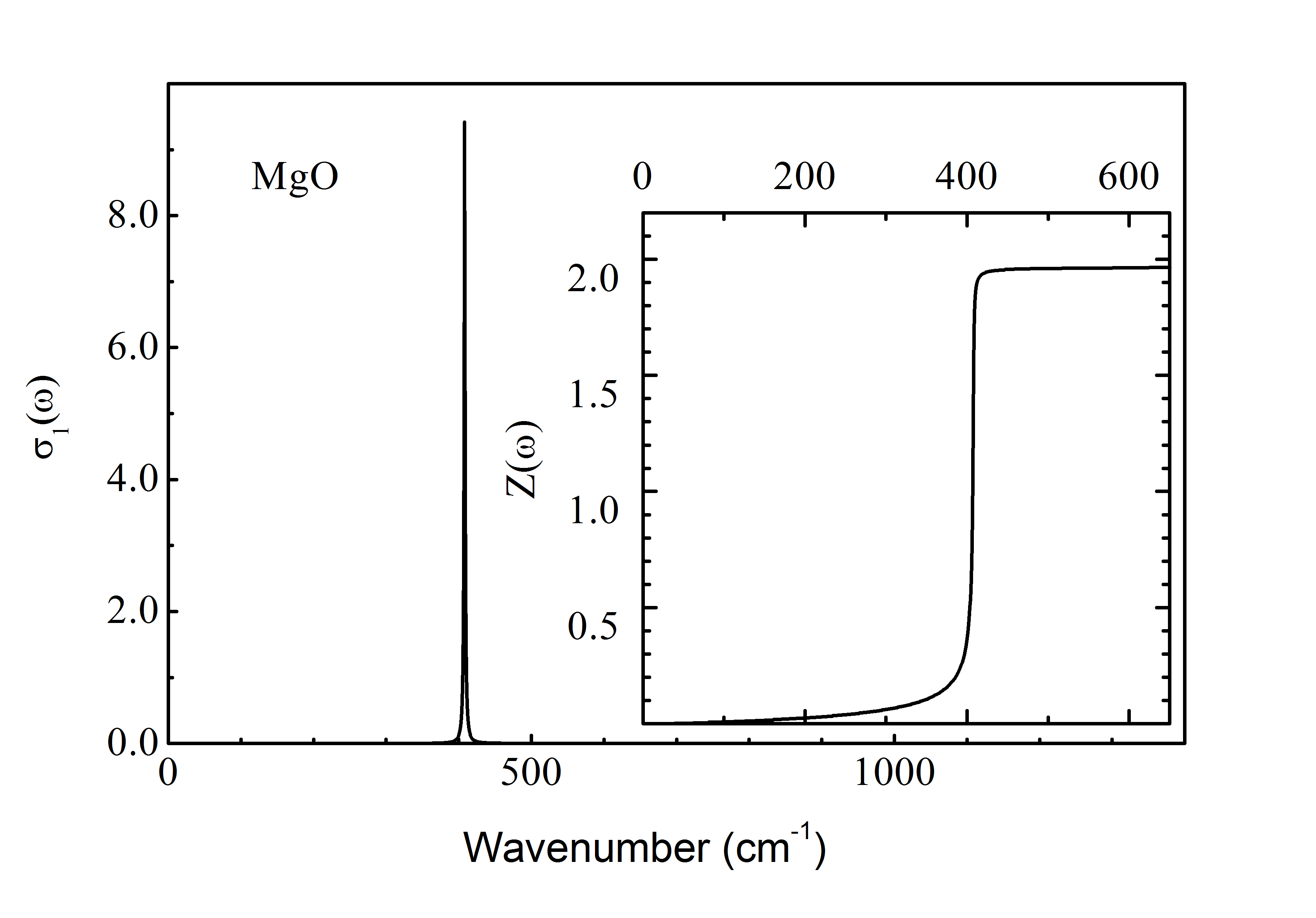
here the index j labels the different species. This sum rule can be applied to measure the charge of ions involved in vibrational modes. If we can separate the contribution to the optical conductivity due to the optical modes we can invert Eq. (131) to calculate the effective charge related to the mode. For example, in MgO (figure 23) both ions contribute an equal charge . We define the effective mass as and assume that the density of the two is equal. In that case we can rewrite Eq. (131) as,
| (132) |
where the integral has to be taken in a frequency range such that it includes the spectral weight of the optical phonon mode but nothing else.
We will now derive expressions for the conductivity sum rule from a more microscopic point of view. To do that we return to the Kubo expression for the optical conductivity,
| (133) |
The Hamiltonian in this expression is that of the system of interacting electrons without the interaction of light. It represents the optical conductivity for the system in an arbitrary (ground or excited) many-body state . A peculiar point of this expression is that although the velocity operators create a single electron-hole pair, due to the fact that the hamiltonian in the denominator of this expression still contains the interactions between all particles in the system, the optical conductivity represents the response from the full collective system of electrons. If we integrate this expression over frequency we get,
| (134) |
We now take a closer look at the right-hand side of this expression. Remember that,
| (135) |
Using the commutator we can rewrite,
| (136) |
Inserting this back into Eq. (134) we find after some rearranging
| (137) |
where stands for the trace over all many-body states. Here we have used that,
| (138) |
and the fact that . We can now obtain different expressions for the sum rule by working out the commutator on the right-hand side of Eq. (137) based on different model assumptions. In table 2 we summarize some results.
| Free electrons | ||
| Band electrons | ||
| N.N. |
The sum rule for band electrons is in practice the most useful. Suppose that we have a system with only a single reasonably well isolated band around the Fermi level that can be approximated by a tight binding dispersion . In that case we find an interesting relation,
| (139) |
This sum rule states that by measuring the optical spectral weight we are in fact measuring the kinetic energy of the charge carriers contributing to the optical conductivity. In real systems this relation only holds approximately: usually there are other bands lying nearby and the integral on the left contains contributions from these as well. Often the bands are described by more complicated dispersion relations in which case the relation does not hold. We can make some other observations from the sum rule for band electrons. Suppose again we have a single empty cosine like band (it is only necessary that the band is symmetric but it simplifies the discussion) at . Since the band is empty, the spectral weight is equal to zero. If we start adding electrons the spectral weight starts to increase until we reach half-filling. If we add more electrons the spectral weight will start to decrease again because the second derivative becomes negative for . If we completely fill the band the contributions from will precisely cancel the contributions from and the spectral weight is again zero. Now consider what happens if we have a half-filled band and start to increase the temperature. Due to the smearing of the Fermi-Dirac distribution higher energy states will get occupied leaving behind lower energy empty states. The result of this is that the spectral weight starts to decrease. One can show using the Summerfeld expansion that the spectral weight follows a temperature dependence. In the extreme limit of something remarkable happens: the Fermi-Dirac distribution is 1/2 everywhere and the electrons are equally spread out over the band. The metal has become an insulator!
IV.3 Applications of sum rules to superconductors
Before we have a look at some applications of sum rules to superconductors we first summarize some results from BCS theory. We want to apply our ideas to cuprate superconductors so we use a modified version from the original theory to include the possibility of d-wave superconductivity. In other words we suppose that there is some attractive interaction between the electrons that has a momentum dependence. The energy difference between the normal and superconducting state due to interactions can be written as marel ,
| (140) |
where and are the pair correlation function and its fourier transform respectively.
We can find an expression for ,
| (141) |
As usual,
| (142) |
and the temperature dependence of is given by,
| (143) |
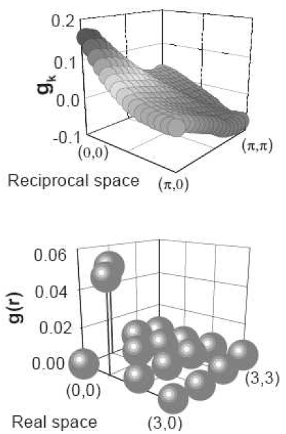
We now use a set of parameters extracted from ARPES measurements to do some numerical simulations. First of all we calculate and fourier transform it to obtain . The results are shown in figure 24.
Although is not so illuminating is. This function is zero at the origin and strongly peaked at the nearest neighbor sites. This is a manifestation of the d-wave symmetry. We also note that the correlation function drops off very fast for sites removed further from the origin.
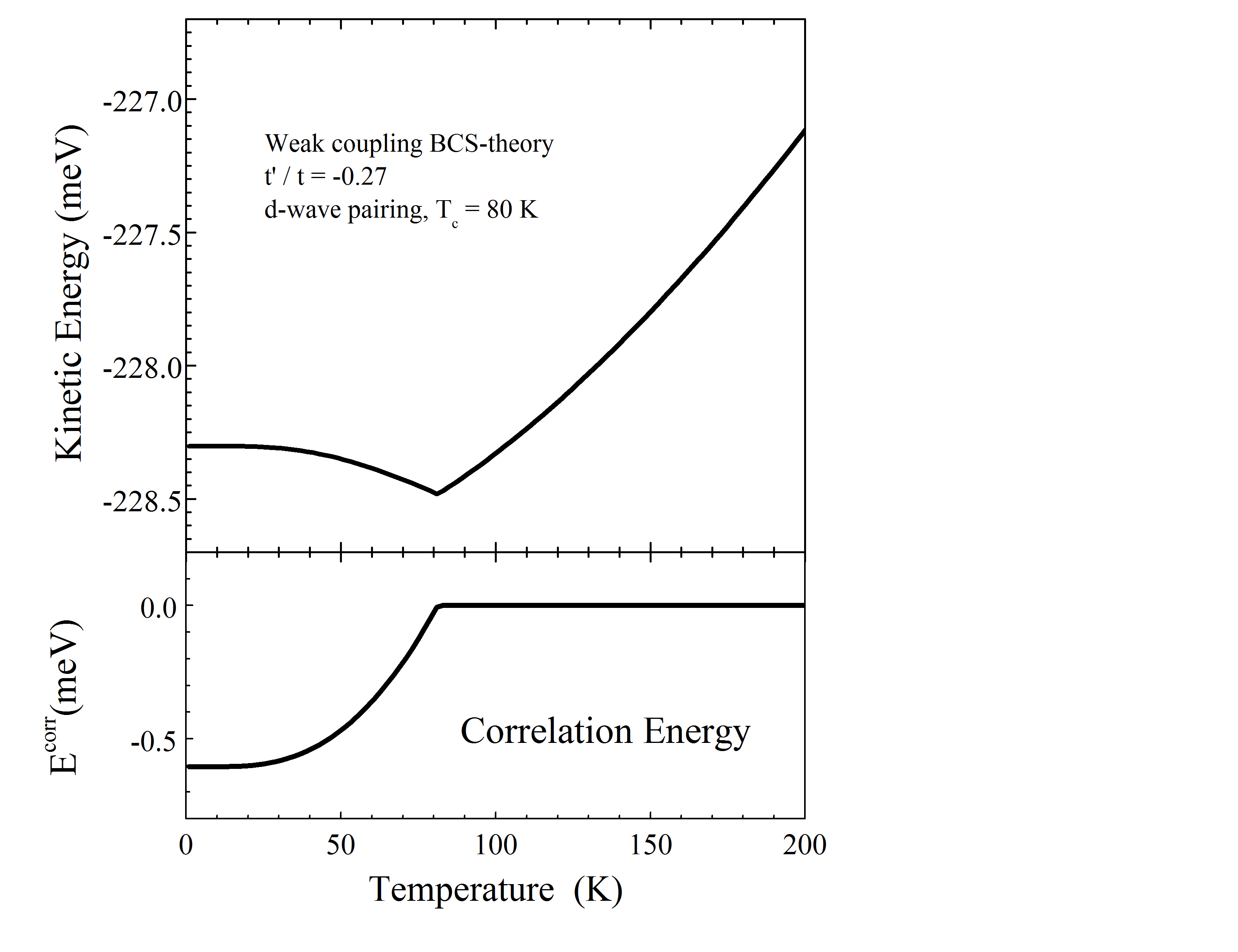
In figure 25 we show the results for a calculation of the correlation and kinetic energy using the parameters extracted from ARPES measurements on Bi-2212. The kinetic energy is calculated from,
| (144) |
We see that the kinetic energy increases in the superconducting state. This can be easily understood by looking at what happens to the particle distribution function below , as indicated in the left panel of figure 26: when the system enters the superconducting state the area below the Fermi energy decreases and the area above the Fermi energy increases thereby increasing the total kinetic energy of the system.
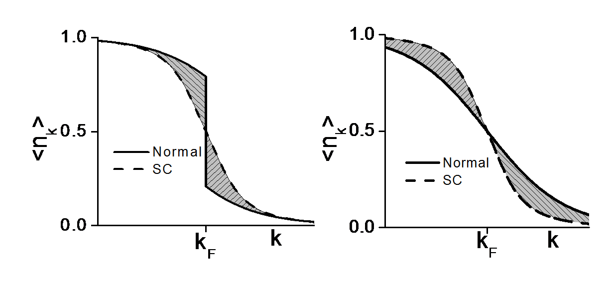
Nevertheless the total internal energy, which is the sum of the interaction energy and the kinetic energy, decreases and this is of course why the system becomes superconducting. Now let us take a look at what happens in the cuprates. In figure 27 we display the optical spectral weight as a function of for Bi-2223.
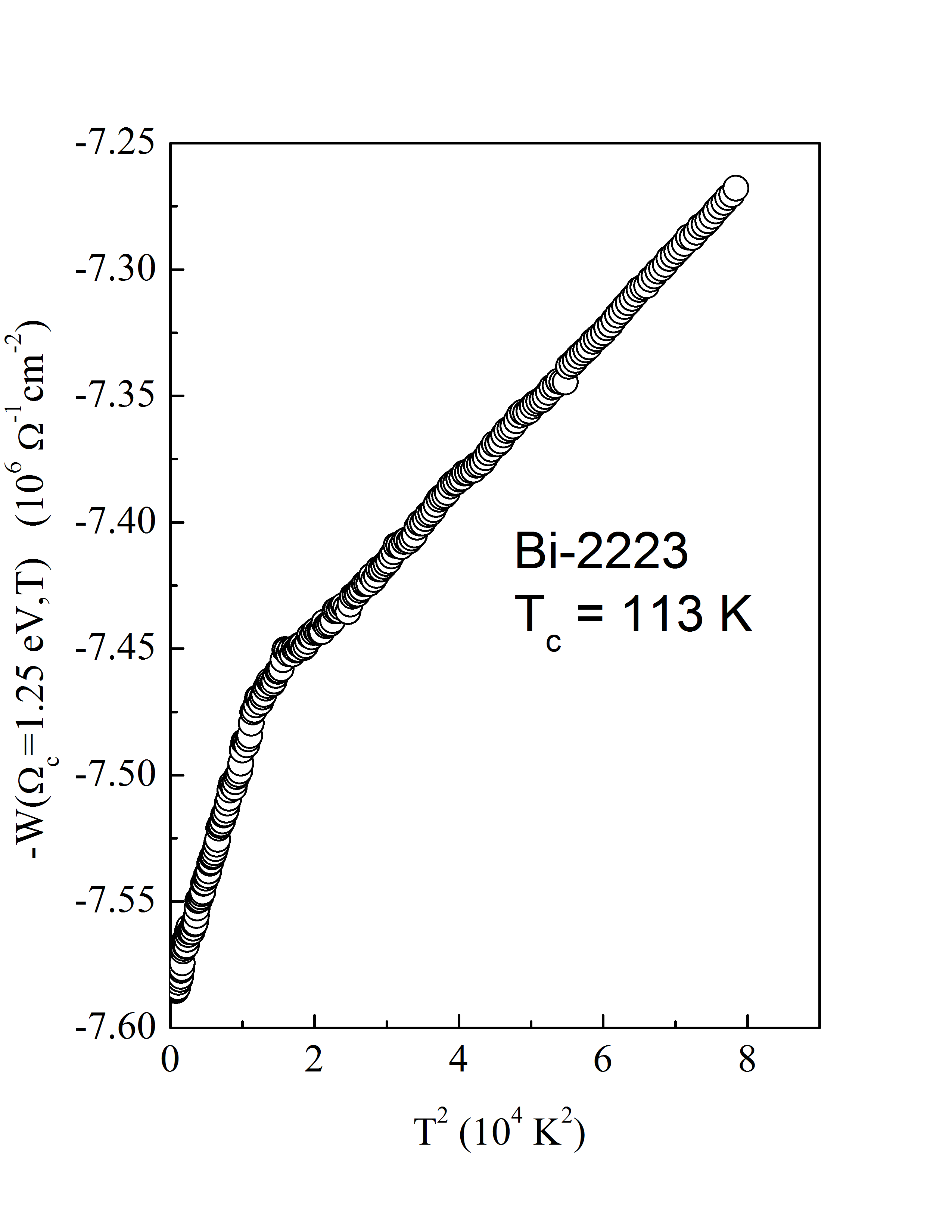
To compare this to the BCS kinetic energy we have plotted here . This result is contrary to the result from our calculation: the kinetic energy decreases in the superconducting state. This experimental result, observed first by Molegraaf et al. molegraaf , has sparked a lot of interest both experimentally heumen ; basov ; syro ; kuz2 ; carbone and theoretically hirsch ; anderson2 ; eckl ; wrobel ; haule ; toschi ; marsiglio ; mayer ; norman . We note that DMFT calculations with the Hubbard model as starting point have shown the same effect as observed here mayer . Roughly speaking the effect is believed to be due to the ”strangeness” of the normal state (right panel figure 26). It is well known that the normal state of the cuprates shows non Fermi-liquid behavior. So if the distribution function in the normal state does not show the characteristic step of the Fermi liquid at the Fermi energy but is rather a broadened function of momentum it is very well possible that the argument we made for the increase of the kinetic energy (see above) is reversed.
IV.4 Applications of sum rules: the Heitler-London model
Another interesting application of sum rules is that we can use them in some cases to extract the hopping parameters of a system. In order to see how this works we express the optical conductivity at zero temperature,
| (145) |
in terms of the dipole operator. Here is the groundstate of the system. To do this we make use of the commutator Eq. (135) and the insertion of a complete set of states. After integrating over frequency we get
| (146) |
We note that this can be done only for finite system sizes. Now consider the special case of a diatomic molecule with two energy levels, one on each atom and a hopping parameter t and distance between the two atoms. We also assume that there is a splitting between the two levels. The hamiltonian for such a system is,
| (147) |
The indices and indicate the left and right atom respectively. If we now put 1 electron in this system we have a two-level problem that is easily diagonalized. As usual we make bonding and anti-bonding states,
| (148) | |||
| (149) |
The coefficients and are given by,
| (150) |
The bonding and anti-bonding states are split by an energy ,
| (151) |
We are now in position to calculate the transition matrix element appearing in Eq. (146). The position operator can be represented by,
| (152) |
So the matrix element is,
| (153) |
Using this in the sum rule Eq. (146) finally gives us the spectral weight of this model,
| (154) |
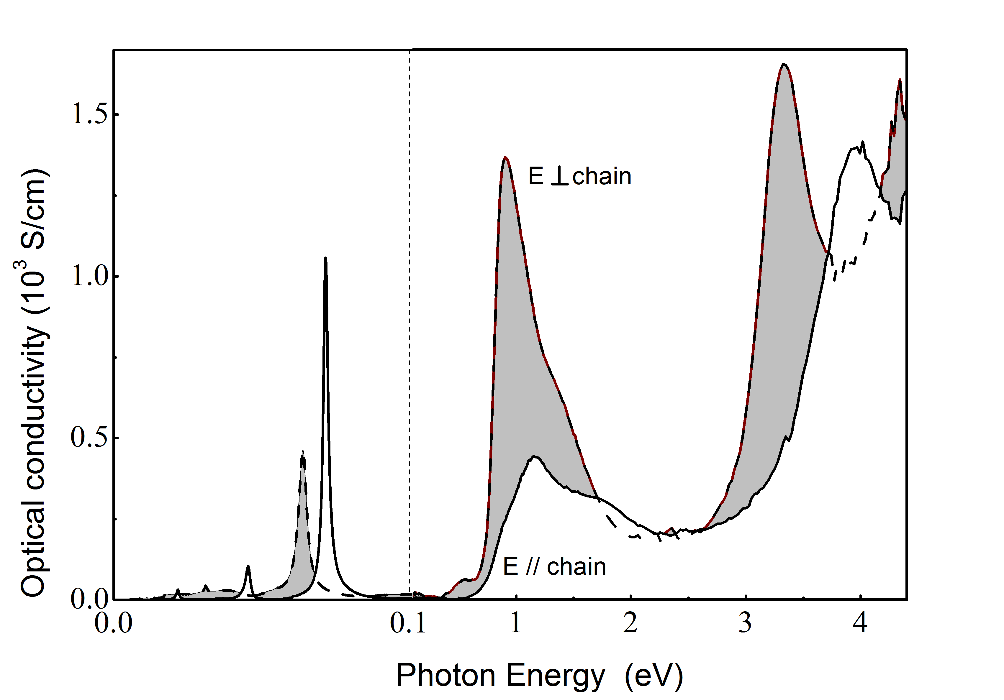
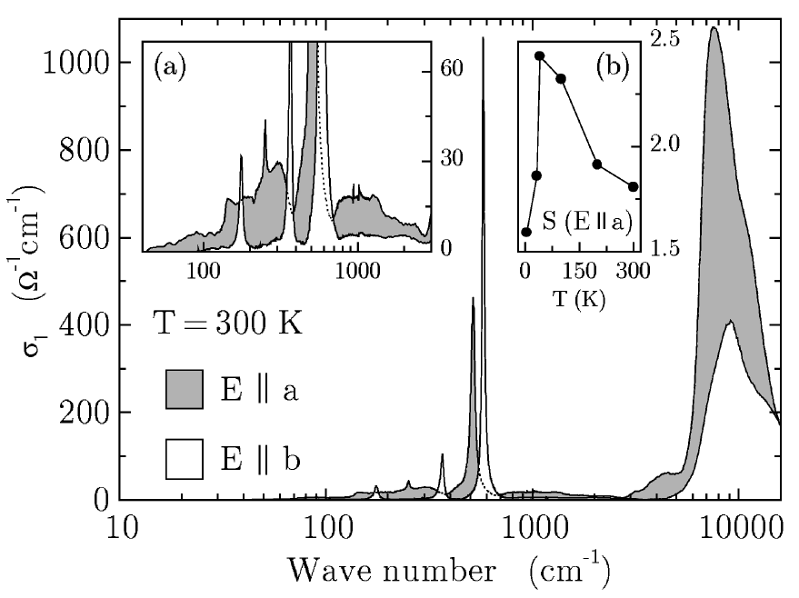
We see that there is a very simple relation between the spectral weight of this model and the hopping parameter. This sumrule has been applied to -NaV2O5 damascelli2 . This compound is a so-called ladder compound. It consists of double chains of vanadium atoms forming ladders which are weakly coupled to each other. Each unit cell contains 4 V atoms and 2 valence electrons. The vanadiums on the rungs of the ladder are more strongly coupled than those along the legs, i.e. . The Heitler-London model we have discussed above can be applied to this system since each rung forms precisely a two level system with different levels. The only difference that we have to take into account is that this is a crystal consisting of independent two level systems. Figure 28 shows the optical conductivity of -NaV2O5.
There are two measurements shown: one with light polarized parallel to the chains and one with light polarized perpendicular to the chains. We can immediately read of eV. Integrating the contribution to the optical conductivity of the peaks we find that the spectral weight perpendicular to the chains is roughly 4 times larger then the spectral weight parallel to the chains, so . Inverting Eq. (154) we can calculate and we find eV. The second strong peak at approximately 3.2 eV is a charge transfer peak from vanadium to oxygen. We will come back to this example in the last section on spin interactions.
IV.5 Generalized Drude formalism
We have already encountered the Drude formula for the optical conductivity of a metal (see the section on polaritons). Even though this model is based on a classical gas of non-interacting particles it describes amazingly well the optical properties of a good metal. This is even more surprising if one realizes that in a metal electrons reside in bands and that the transitions we are making with photons are vertical due to the negligible photon momentum. So from the band picture point of view, when we consider a single band of electrons interacting with photons we should expect a single delta function at the origin. The reason that this is not what is observed is because we have neglected the other interactions in the system. Electrons in solids interact with the lattice vibrations, impurities and/or other collective modes. Due to the electron-phonon interaction for instance we can have processes where a photon creates an electron-hole pair in which the electron ”shakes off” a phonon. In this process the phonon can carry away a much larger momentum then originally provided by the photon. Due to this effect we can have phonon-assisted transitions which give a width to the delta function. This width is called the scattering rate. If the interactions are inelastic, as in the interactions with impurities, this scattering rate is just a constant. Otherwise, this scattering rate can depend on frequency. However, if we define the scattering rate in Eq. (58) to be frequency dependent, , the KK-relations force us to introduce a frequency dependent effective mass as well. This is what is done in the generalized Drude formalism Allen . The optical conductivity is written as,
| (155) |
Having measured a conductivity spectrum we can invert these equations to calculate 1/ or via,
| (156) |
and
| (157) |
In the last equality of these equations we have defined an optical self-energy. Note that this quantity is not equivalent to the self-energy used in the context of Green’s functions. We can rewrite the optical conductivity in terms of as,
| (158) |
In the case of impurity scattering is simply given by
| (159) |
so that and . We can also capture the effect of the interaction of the electrons with the static lattice potential in a self-energy,
| (160) |
which gives and . This is also called static mass renormalization. Finally we consider dynamical mass renormalization where the electrons couple to a spectrum of bosons,
| (161) |
Here is a coupling constant and is a characteristic temperature scale related to the bosons. In this case we find,
| (162) |
and
| (163) |
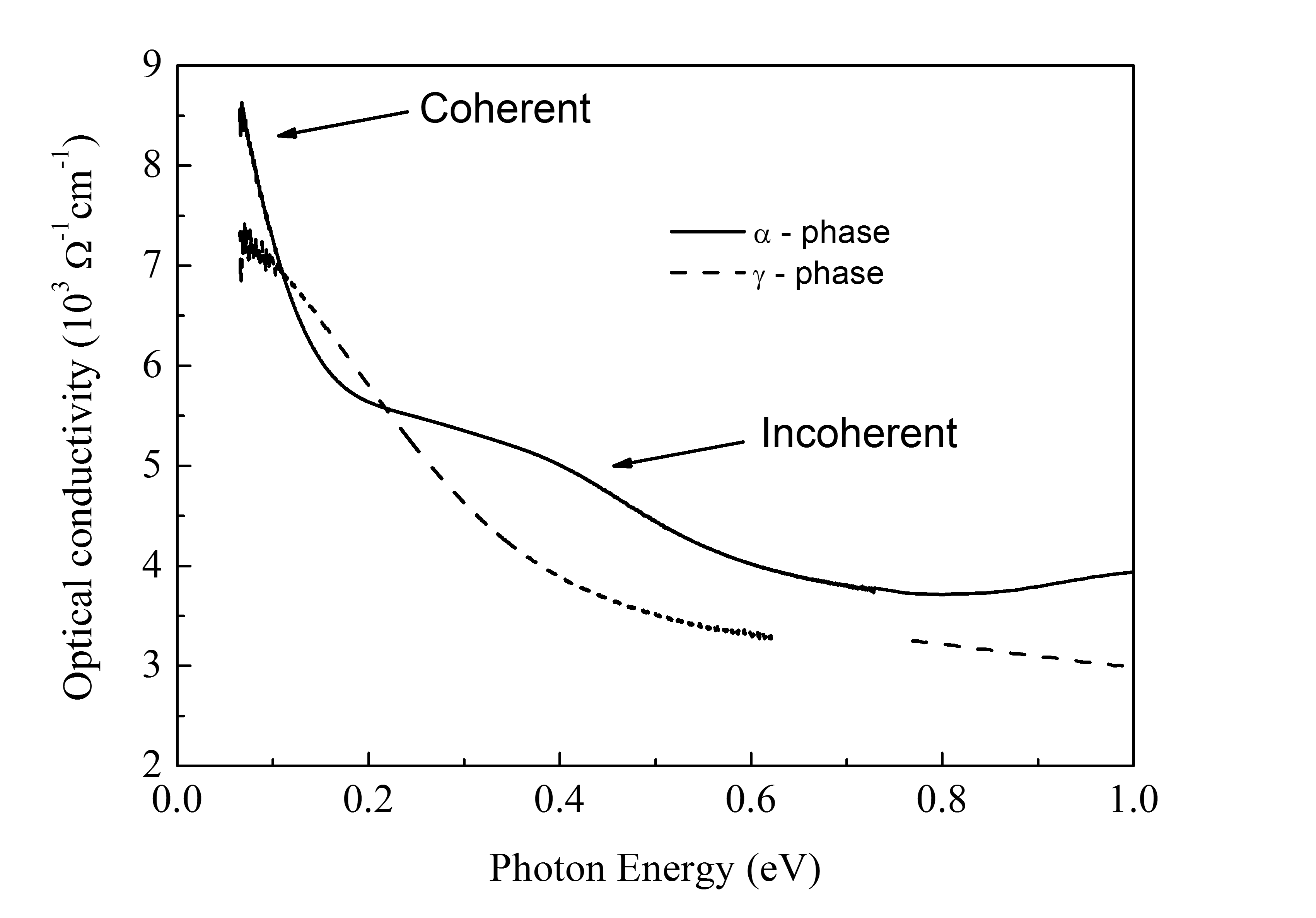
As an example we will discuss the -phase to -phase transition in pure Cerium. When Cerium is grown at elevated temperatures it forms in the so called -phase. At low temperatures a volume collapse occurs and the resulting phase is called the -phase. This iso-structural transition is first order. The reduction in volume can be as much as 20 to 30 . Ce has 4 valence electrons and these can be distributed between
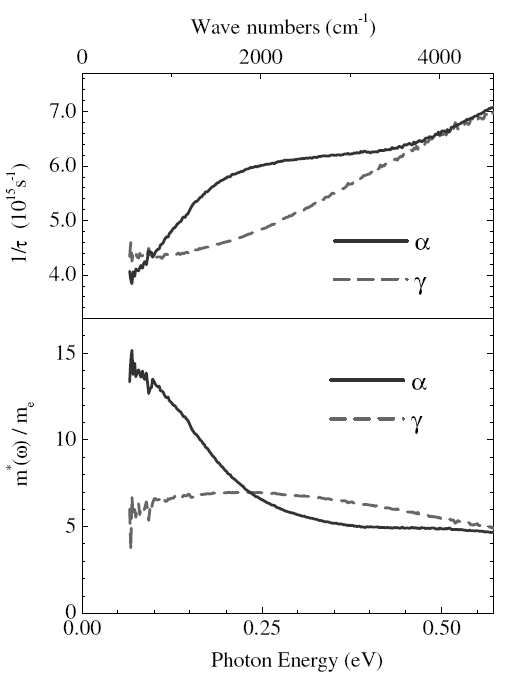
localized states and the states that form the conduction band. If occupied, the 4f states will act as paramagnetic impurities. In the -phase the Kondo temperature 100 K whereas in the -phase 2000 K. This difference can be understood to be simply due to the larger lattice spacing in the -phase: the hopping integral is smaller and hence is smaller. Figure 29 shows the optical conductivity of - and -Cerium. These measurements were done by depositing Ce films on a substrate at high and low temperature to form either the or phase. We see that -Cerium is less metallic than -Cerium. In the -phase there is only a weak Kondo screening of the impurity magnetic moments and this gives rise to spin flip scattering, which is the main source of scattering. In the -phase the moments are screened and form renormalized band electrons in a very narrow band. This suppresses the scattering. The difference in scattering rates shows up in the optical conductivity as a narrower Drude peak for the -phase (see figure 29). Figure 30 displays the scattering rate and effective mass extracted from the optical conductivity in figure 29 using Eq. (156) and (157). In the -phase extrapolates to a finite value due to local moment or spin-flip scattering. We can rewrite the real part of the optical conductivity in Eq. (158) with the self-energy of Eq. (161) as follows,
| (164) |
Note that we have defined a renormalized plasma frequency, , since the spectral weight is not conserved when adding to . With some simple algebra this can be rewritten as,
| (165) |
It follows that the real part of this expression is then,
| (166) |
We see that the optical conductivity is split into two contributions: a -function which represents the coherent part of the charge response and an incoherent contribution. The -function is usually broadened due to other scattering channels present in the system. In this case the -function represents the contribution due to the Kondo-peak whereas the incoherent contribution is due to the side-bands. This splitting of the conductivity in a coherent and incoherent contribution is nicely observed in the -phase of Cerium as indicated in figure 29.
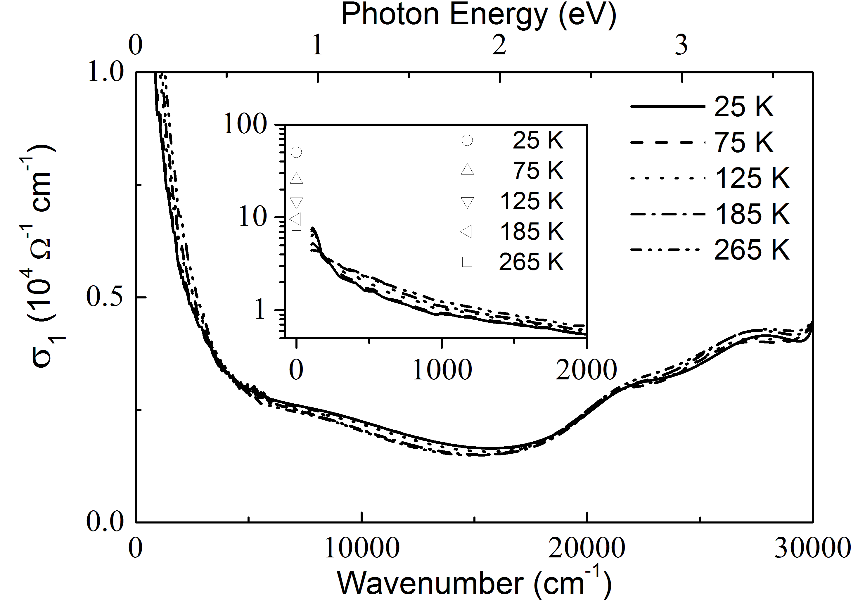
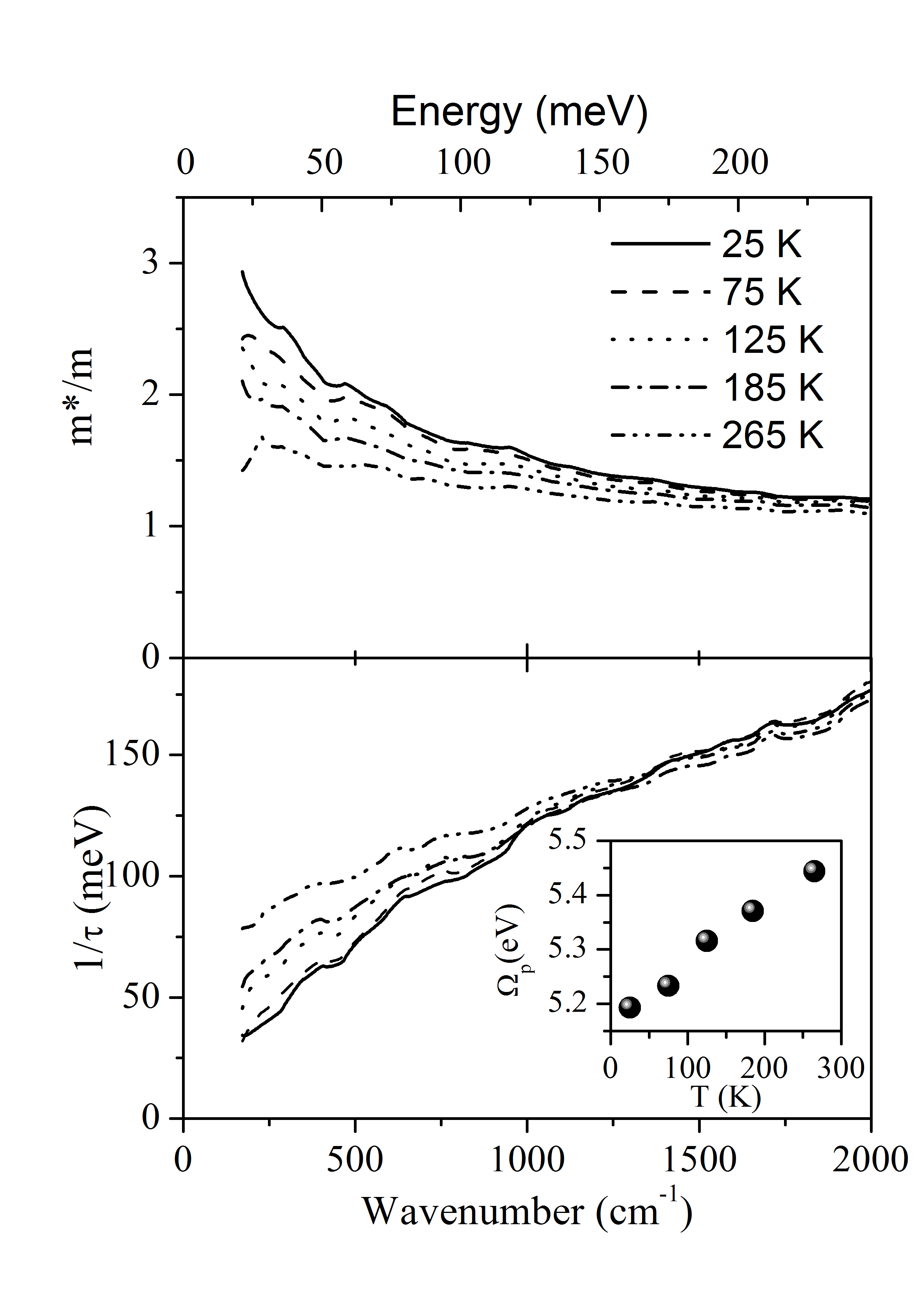
This splitting of the optical conductivity in coherent and incoherent contributions is much more general however and is frequently observed in correlated electron systems.
V Electron-phonon coupling
Electron-phonon coupling is most easily described in the framework of Migdal-Eliashberg theory. The application of the theory to optics can be found in the papers by Allen Allen . In the so-called Allen approximation the self-energy in Eq. (158) is calculated using,
| (167) |
Here the kernel is given by,
| (168) |
where the are Digamma functions. The function appearing in Eq. (167) is the phonon spectral function. The label ”tr” stands for transport indicating that the spectral function is related to a transport property. This function is different by a multiplicative factor from the true as measured by for instance tunnelling. The electron-phonon coupling strength is easily calculated from by integration,
| (169) |
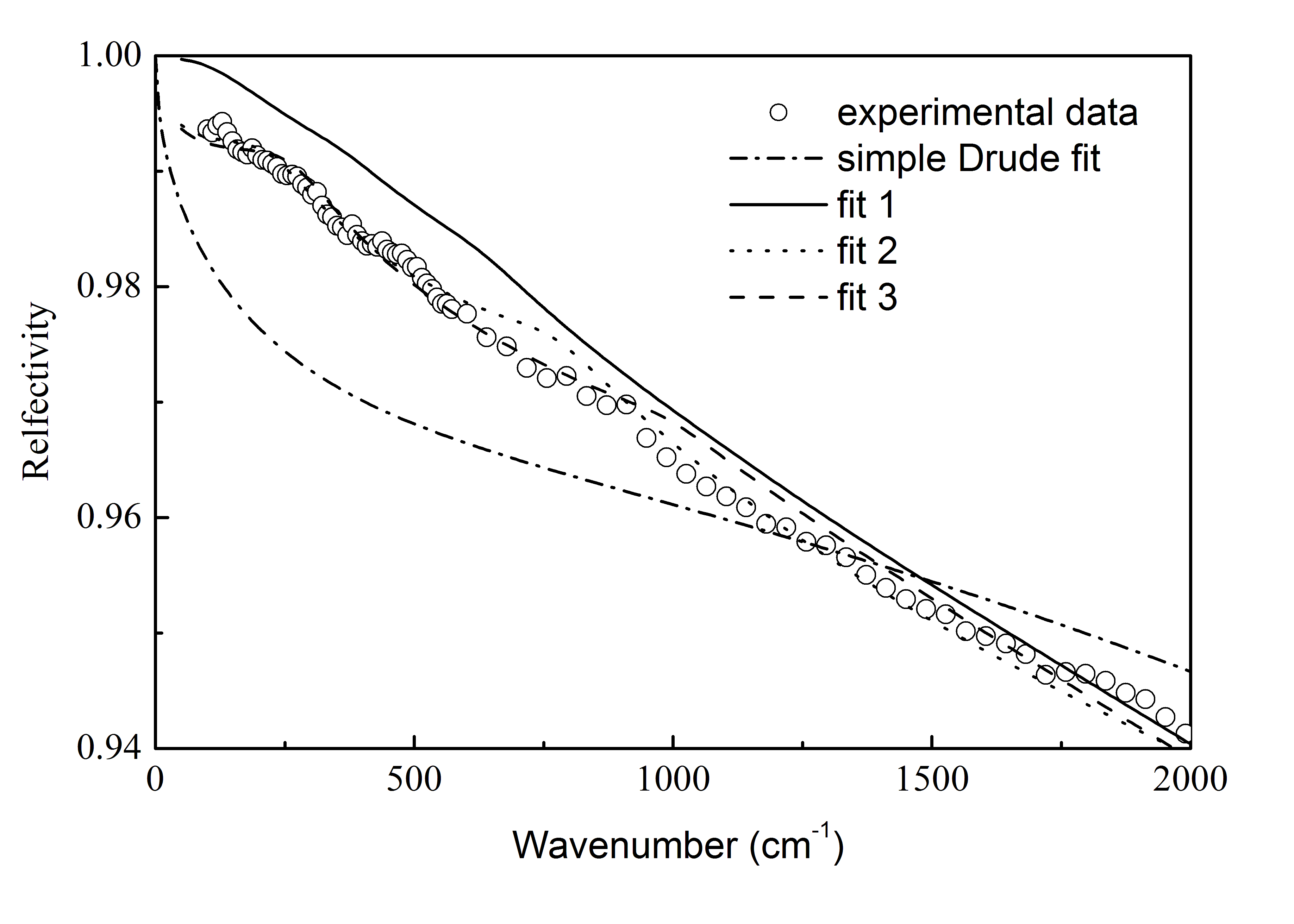
This approach was first applied by Timusk and Farnworth in a comparison of tunnelling and optical measurements on the superconducting properties of Pb Timusk . As an example we discuss the application of this formalism to the optical properties of ZrB12 teyssier . Figure 31 shows the optical conductivity of ZrB12. The spectrum consists of what appears to be a Drude peak and some interband contributions. Also shown are the calculated and . The temperature dependence of is what is usually observed for a narrowing of the Drude peak with decreasing temperature whereas the strong frequency dependence is suggestive of electron-phonon interaction. Using the McMillan formula (169) the coupling strength was estimated to be . In figure 32 the reflectivity of ZrB12 together with calculations based on Eq. (158) and (167) is shown. It is clear that a simple Drude form is not capable of describing the observed reflectivity. The first fit (fit 1) is a fit where the that was used as input was derived from specific heat measurements Lortz . Although it gives an improvement over the standard Drude fit there is still some discrepancy between the data and the fit. To make further improvements was modelled using a sum of -functions. The results of this modelling are indicated as fit 2 and fit 3. Using Eq. (169) we find coupling strengths 1 - 1.3. Another method to roughly estimate is due to Marsiglio Marsiglio1 ; Marsiglio2 . It states that a rough estimate of the shape of can be found by simply differentiating the optical data,
| (170) |
where is the plasma frequency. The obvious problem with this method is that it requires the double derivative of the data. Because of the inevitable noise in the data usually some form of smoothing is required. Applied to ZrB12 the extracted shows peaks at the same positions as the ones extracted before and a coupling strength . These results indicate a medium to strong electron-phonon coupling for ZrB12.
VI Polarons
There exist many definitions of what is a polaron. Electrons coupled to a phonon have been called polaron as have free electrons moving around in an insulator. Here we will consider the Landau-Pekar approximation for a polaron landau ; landau2 . The idea is that when an electron moves about the crystal it polarizes the surrounding lattice and this in turn leads to an attractive potential for the electron. If the interaction between electron and lattice is sufficiently strong this potential is capable of trapping the electron and it becomes more or less localized. The new object, electron plus polarization cloud is called polaron. This self-trapping of electrons can occur in a number of different situations and different names are used. For instance, one talks about small polarons in models where only short range interactions are considered, because this typically leads to polaron formation with polarons occupying a single lattice site. From the Landau-Pekar formalism we can get some feeling of when polarons form and what their
properties will be. First of all, the coupling constant is given by,
| (171) |
where stands for the unit Rydberg (1 Rydberg = = 13.6 eV), is the oscillator frequency of the (Einstein) phonon mode involved and are the band and free electron mass respectively and is given by,
| (172) |
For strong coupling (small polarons) the polaron mass is expressed in terms of the coupling constant as,
| (173) |
with the polaron binding energy given by,
| (174) |
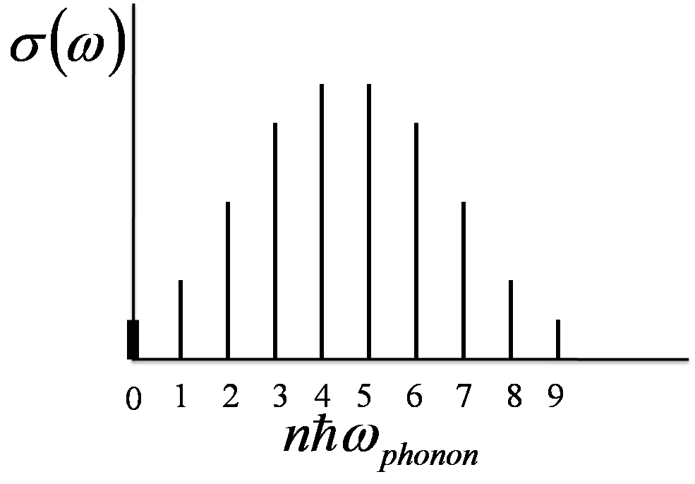
The polaron binding energy typically is of the order of a few 100 meV. The polaron mass is typically of the order of 50-100 times the electron mass. The effect of polaron formation on the optical conductivity can be described by assuming a gas of non-interacting polarons (i.e. low polaron density). This results in a spectrum that can be described by a Drude peak and a so-called Holstein side-band. If we assume that the electrons interact with a single Einstein mode the spectrum will look as in figure 33. The spectrum consists of a zero-phonon, coherent part (n = 0) with a spectral weight 1/(1+0.02) followed by a series of peaks that describe the incoherent movement of polarons assisted by n=1,2,3.. phonons. In real solids the peaks are smeared out due to the fact that phonons form bands. The real part of the optical conductivity can thus be described as,
| (175) |
The first term in this expression describes the coherent part of the spectrum, which in real solids will also be smeared out to finite frequency by other forms of scattering, and an incoherent term given by the second term which is called the Holstein band. The shape of the side-band can be qualitatively understood by imagining how a polaron has to move through the lattice. In order to move from one site to another the lattice deformation around the original site has to relax and be adjusted on the new site. This relaxation process results in the multi-phonon side-bands of the Drude peak.
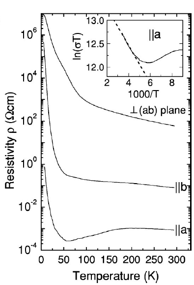
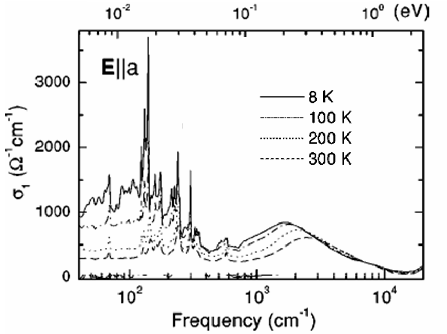
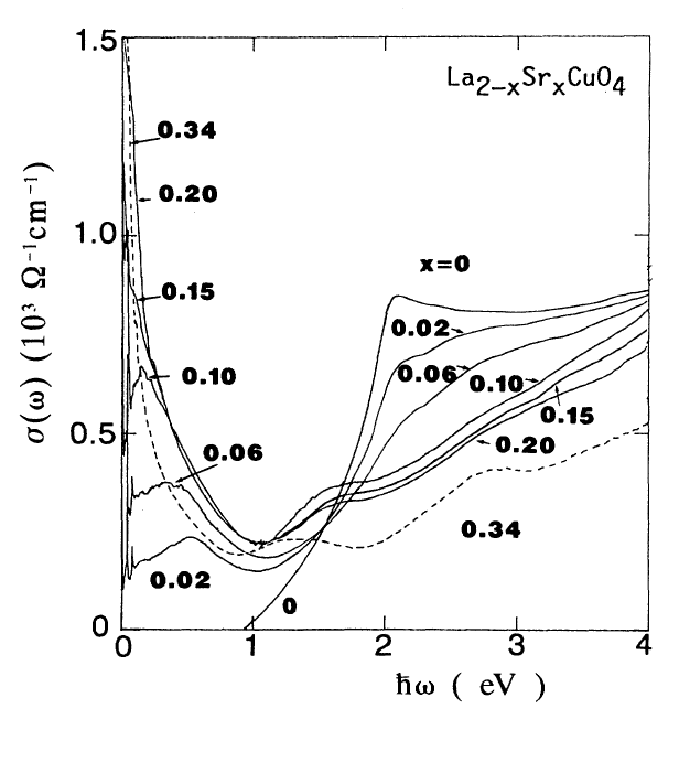
The observation of the Holstein side-band is somewhat complicated because it is not possible to distinguish between normal interband transitions and the effects due to polaron formation. There have been some claims that a band observed in the mid infrared region ( 100 - 500 meV) of the spectrum of high-Tc superconductors is due to polaron formation but many other interpretations exist. Figure 34 shows the doping dependence of La2-xSrxCuO4. The peak that occurs around 0.5 eV for the 0.02 doped sample has been interpreted as the Holstein side-band. Another example where polarons could play a role is in LaTiO3.41 kuntscher . In this material the resistivity (figure 35) shows a quasi one dimensional behavior with an upturn of the resistivity at lower temperatures. This could be due to polaron formation but it has also been interpreted as due to a charge density wave. The optical conductivity at low temperatures shows that a large part of the spectral weight is contained in a side-band around 300 meV (see figure 35). If this peak would be due to polarons we expect that when we warm up the system to higher temperatures its spectral weight should be diminished. This is because the increased temperature unbinds electrons from their self-trapping potential and therefore shifts spectral weight from the Holstein band to the Drude peak. This is also what is observed and at the same time explains the decrease of resistivity with increasing temperature.
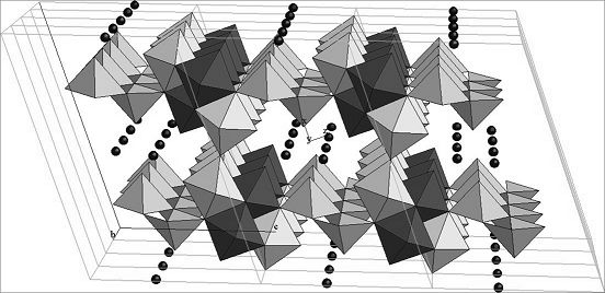
The last example we will discuss is NaV6O15. The structure of this compound is build up out off octahedra and tetrahedra of vanadium and oxygen atoms where the tetrahedra form quasi 1-dimensional zig-zag chains (see figure 36). There are 3 different types of vanadium sites in this structure: 2 of them are ionic with a charge 5+ on the vanadium which has then a configuration. The third site has half an electron more leading to a charge of 4.5+ on the vanadium atom in a configuration. Because of this we expect a quarter filled band and metallic behavior. Figure 37 shows the optical conductivity of - NaV6O15. The chains are along the direction labelled b. At energies around 3000 cm-1 we observe a broad peak for light polarized along the -direction which could be due to polarons although these transitions also correspond well with the energies predicted by the Hubbard model for d-d transitions. If we compare the conductivity with polarization parallel and perpendicular to the b-axis, we see that the conductivity perpendicular to the b-axis is insulating whereas the one along the b-axis is conducting. This conducting behavior is due to the quarter filled bands.
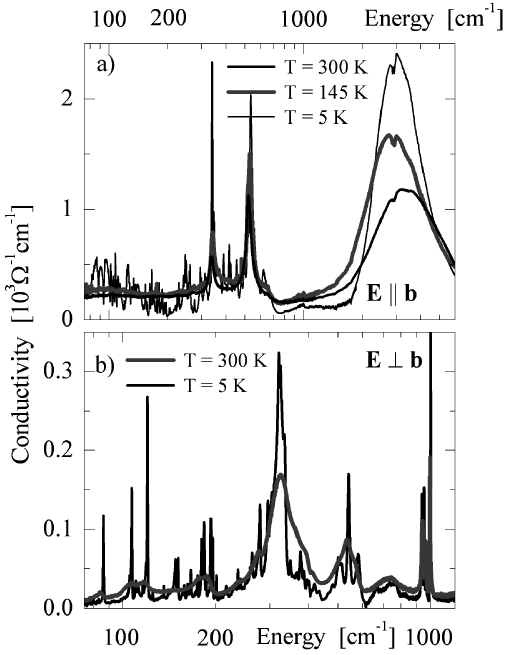
Are polarons playing an important role in the above examples ? It is nearly impossible to answer this question experimentally due to the above mentioned difficulty in separating polaronic behavior from normal interband transitions. Moreover, in most cases where polarons are invoked, other theories are also able to reproduce the experimental results. To close this section we briefly discuss what happens if the density of polarons becomes larger. Imagine what happens if we increase the density of polarons such that we are getting close to a system with one polaron on each site. In that case the original lattice will almost be completely deformed and one can wonder wether the electrons are still capable to self-trap. It seems reasonable that in this limit the polaron picture no longer applies. Another possibility is the formation of bipolarons. Since the deformation energy of the lattice is proportional to the electron charge , the binding energy of two polarons is . The binding energy of a bipolaron (two electrons trapped by the same polarization cloud) is twice as large however . This binding energy is usually not enough to overcome the Coulomb repulsion between the electrons.
VII Spin interactions
As mentioned in the previous section the signatures for the presence of polarons can often be interpreted with different ideas. Most often these models are based on coupling to magnetic interactions. Consider for example the spectrum of the parent (undoped) compound YBa2Cu3O6 which is a Mott insulator (see bottom panel of figure 14). Below 100 meV we see a series of peaks which are due to phonons. But what about the structure between 100 meV and 1 eV ? One of the difficulties in explaining this structure is that light does not directly couple to spin degrees of freedom. It is however possible to indirectly make spin flips with photons (see figure 38).
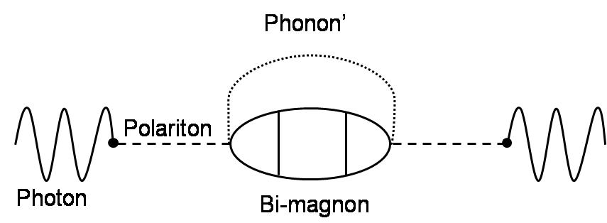
For this process to occur we have to include phonon-magnon interaction. When a photon enters the material it gets dressed with phonons forming a polariton which is then coupled to the spin degrees by the phonon-magnon interaction. This leads to the possibility of so-called phonon assisted absorption of spin-flip excitations Lorenzana . We see from figure 38 that the polariton creates a bi-magnon. This is because the intermediate state has to have spin S = 0. The dashed square represents all magnon-magnon interactions. The coupling constant for this process was first calculated by Lorenzana and Sawatzky and is
| (176) |
where is the superexchange constant and is the atomic displacement vector. In the process momentum and energy have to be conserved and this leads to
| (177) |
and
| (178) |
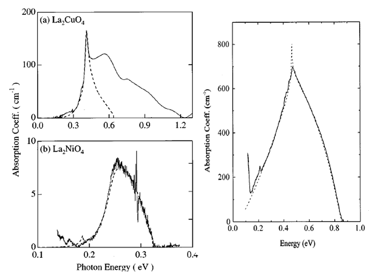
for the process in figure 38. This gives constraints on the possible absorptions. In figure 39 some examples are shown of materials in which we believe this process to play a role. One of the compounds where the predicted optical conductivity fits the spectrum very well is in the case of Sr2CuO3. To make the fit the magnon dispersion as measured with neutron scattering was used. The reason that this theory works so well for Sr2CuO3 is that the conduction is nearly one dimensional. This gives a good starting point because the magnon spectrum is completely understood. On the contrary, the theory is not completely capable of predicting the spectrum of La2CuO4. Most likely the peaks around 0.6 and 0.75 eV are due to 4 and 6 magnon absorption. In the case of YBa2Cu3O6 the situation gets even more complicated due to the presence of two layers per unit cell. Because of the doubling of the unit cell, there are now acoustic and optical magnon branches just as what would happen in the case of phonons. The effect of this on the optical conductivity was first discussed by Grueninger et al. Grueninger ; Grueninger2 .
Another example of probing of spin excitations occurs in NaV2O5. As already discussed in the previous section this compound has quasi one dimensional chains as shown in figure 36. These chains can be seen to form a so-called ladder structure, with the ladders parallel to the direction.
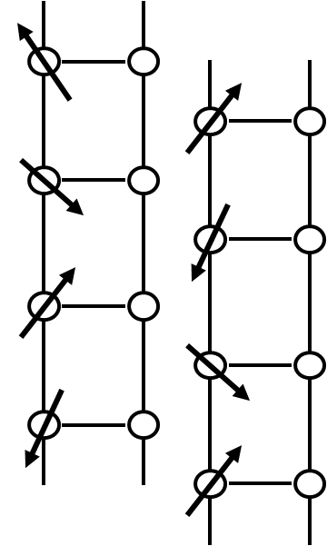
Each adjacent ladder is shifted with respect to the previous such that the rungs of one ladder fall in between those of the next (figure 40). The vanadium atoms that form the ladders have an average charge of +4.5. It has been claimed carpy that the charge distribution is inhomogeneous with most of the charge on one side of the ladder as indicated in figure 40.
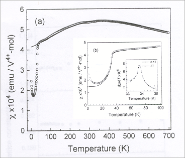
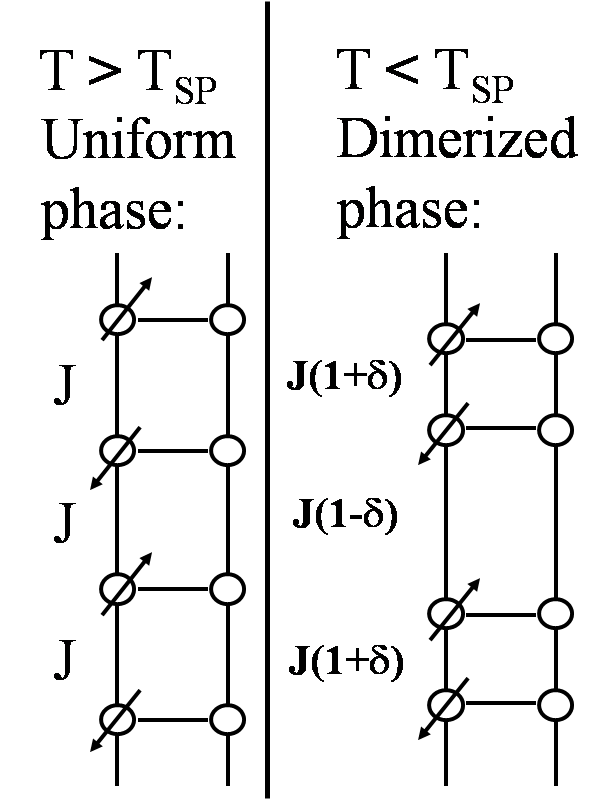
The temperature dependence of the magnetic susceptibility can be modelled pretty well using a Bonner-Fischer model for a spin-1/2 Heisenberg chain Isobe for temperatures higher then 34 K (see figure 42). Below 34 K, X-ray analysis shows a doubling of the a- and b- axes and a quadrupling of the c-axis. It indicates that the new unit cell consists of 64 vanadium atoms and 32 valence electrons. At the same temperature the susceptibility shows an abrupt drop. An explanation for this transition is in terms of a spin-Peierls transition. In the high temperature phase (T TSP) the left side of the ladder has a uniform spin distribution, as indicated in the left panel of figure 42, which is reasonably well described with an anti-ferromagnetic (AF) S = 1/2 Heisenberg spin chain with uniform exchange coupling . For T TSP the system dimerises due to a deformation of the lattice, leading to an alternation of exchange couplings (see right panel figure 42). Here we focus on the high temperature phase. If the charge inhomogeneity is present it would lead to a breaking of the inversion symmetry which in turn leads to a non-zero optical matrix element for two magnon absorption damascelli3 . The idea is similar to the Lorenzana-Sawatzky model discussed above. In the latter case the phonon effectively lowers the symmetry making the process optically allowed. The optical conductivity of - NaV2O5 is shown in figure 43. We can model - NaV2O5 with independent ladders where the hopping probability along a rung () is much larger than that along the ladder (). Furthermore we assume a large on-site repulsion U. We can then model a ladder by independent rungs. Assuming a quarter filled ladder (one electron per rung) we have a simple two level problem leading to bonding and anti-bonding levels (see also the discussion in the section on applications of sum rules). If we also include a potential energy difference between the sites the wavefunctions become asymmetric with higher probability on the low potential site and one can show that this again leads to bonding and anti-bonding solutions which are split by an energy damascelli3 ,
| (179) |
Transitions from the bonding to anti-bonding band are optically active and involve charge transfer (CT) from the left side of the ladder to the right. The large peak seen in figure 43 around 1 eV is due to these transitions. The energy position of the peak indirectly gives evidence for the charge inhomogeneity: band structure calculations and exact diagonalization of finite clusters give 0.35 eV, which would put the charge transfer peak around 0.7 eV. The observed value of 1 eV thus indicates 0. The spectral weight of the peak allows us to make an estimate for . One can show that,
| (180) |
Using Eq. (179) we find 0.3 eV and 0.8 eV. Besides the large CT peak seen in figure 43 there is also a broad continuum in the infrared region of the spectrum for (see inset). This part of the spectrum can be understood if we include the coupling between rungs of the ladder. For parallel spins on different rungs this coupling would have no effect since the Pauli principle would forbid hopping between the sites. For an anti-parallel spin configuration the system can gain some kinetic energy from virtual hopping of an electron from one rung to the next, putting two electrons on one rung. For very large U this electron would occupy the righthand side of the rung. Starting from an anti-parallel configuration a spin-flip transition on one rung thus leads to a net dipole displacement which leads to optical activity of this transition. We note that because of spin conservation rules we have to make two spin-flips. These excitations have been dubbed charged bi-magnon excitations.
References
- (1) F. Wooten, Optical Properties of Solids (Academic Press, New York, 1972).
- (2) M. Dressel and G. Grunner, Electrodynamics of Solids: Optical Properties of Electrons in Matter (Cambridge University Press, 2002)
- (3) A.A. Tsvetkov et al., Phys. Rev. B 60, 13196 (1999).
- (4) D. van der Marel et al., Proc. of the 10th Anniv. HTS Workshop on Physics, Materials and Applications, Houston, Texas, 1996, edited by B. Batlogg, C.W. Chu, W.K. Chu, D.U. Gubser, and K.A. Muller, World Scientific, Singapore, 1996, pp. 357.
- (5) E. van Heumen et al., Phys. Rev. B 75, 054522 (2007).
- (6) M. Grueninger, Ph.D. thesis University of groningen.
- (7) J.L.M. van Mechelen et al., Phys. Rev. Lett. 100, 226403 (2008).
- (8) A.B. Kuzmenko et al., Phys. Rev. Lett. 91, 37004 (2003).
- (9) P.W. Anderson, Phys. Rev. 110, 827 (1958); P.W. Anderson, Phys. Rev. 130, 439 (1963); P.W. Higgs, Phys. Rev. Lett. 13, 509 (1964); P. W. Higgs, Phys. Rev. Lett. 145, 1156 (1967). See also D. van der Marel, Journal of Superconductivity, 17, 559 (2004).
- (10) J. Zaanen, G.A. Sawatzky, J.W. Allen, Phys. Rev. Lett. 55, 418 (1985).
- (11) D. Y. Smith, E. Shiles, Phys. Rev. B 17, 4689 (1978).
- (12) M. Tinkham, and R. A. Ferrell, Phys. Rev. Lett. 2, 331 (1959).
- (13) A. Damascelli, K. Schulte, D. van der Marel, and A.A. Menovsky, Phys. Rev. B 55, R4863 (1997)
- (14) D. van der Marel, H.J.A. Molegraaf, C. Pressura, Chapter in ”Concepts in electron correlation”, Edited by A. Hewson and V. Zlatic, Kluwer (2003), p 7-16. ; cond-mat/0302169.
- (15) H.J.A. Molegraaf et al., Science 295, 2239 (2002).
- (16) D.N. Basov, S.I. Woods, A.S. Katz, E.J. Singley, R.C. Dynes, M.Xu, D.G. Hinks, C.C. Homes, M. Strongin, Science 283, 49 (1999).
- (17) A.F. Santander-Syro, R.P.S. Lobo, N. Bontemps, Z. Konstatinovic, Z.Z. Li, H. Raffy. Europhys. Lett. 62, 568 (2003).
- (18) A.B. Kuzmenko, H.J.A. Molegraaf, F. Carbone, and D. van der Marel, Phys.Rev.B 72, 144503 (2005).
- (19) F. Carbone et al., Phys. Rev. B 74, 024502 (2006).
- (20) J. E. Hirsch, Physica C 199, 305 (1992).
- (21) P.W. Anderson et al., J. Phys.: Condens. Matter 16, 755(R) (2004).
- (22) T. Eckl, W. Hanke and E. Arrigoni, Phys. Rev. B 68, 014505 (2003).
- (23) P. Wróbel, R. Eder and P. Fulde, J. Phys.: Condens. Matter 15, 6599 (2003).
- (24) K. Haule and G. Kotliar, cond-mat/0601478.
- (25) A. Toschi et al., Phys. Rev. Lett. 95, 097002 (2005).
- (26) F. Marsiglio, Phys. Rev. B 73, 064507 (2006)
- (27) Th.A. Maier, M. Jarrell, A. Macridin, and C. Slezak, Phys. Rev. Lett. 92, 27005 (2004).
- (28) M.R. Norman, C. Pépin, Phys. Rev. B 66, 100506(R) (2002)
- (29) A. Damascelli et al., Phys. Rev. Lett. 81, 918 (1998).
- (30) J.W. Allen and J. C. Mikkelsen, Phys. Rev. B 15, 2952 (1977).
- (31) J.E. van der Eb et al., Phys. Rev. Lett. 86, 3407 (2001).
- (32) B. Farnworth and T. Timusk, Phys. Rev. B 14, 5119 (1976).
- (33) J. Teyssier et al., accepted for Phys. Rev. B, cond-mat/0609426.
- (34) R. Lortz et al., Phys. Rev. B 72, 024547 (2005).
- (35) F. Marsiglio, T. Startseva, J. Carbotte, Phys. Lett. A 245, 172 (1998).
- (36) F. Marsiglio, J. of Superconductivity, 12, 163, (1999).
- (37) L.D. Landau, Phys. Z. Sowjetunion, 3, 644 (1933).
- (38) L.D. Landau and S. Pekar, J. Exptl. Theor. Phys. 18, 419 (1948).
- (39) Uchida et al., Phys. Rev. B 43, 7942 (1991).
- (40) C. A. Kuntscher, D. van der Marel, M. Dressel, F. Lichtenberg and J. Mannhart, Phys. Rev. B 67, 035105 (2003).
- (41) C. Presura et al., Phys. Rev. Lett. 90, 026402 (2003)
- (42) J. Lorenzana and G.A. Sawatzky, Phys. Rev. Lett. 74, 1867 (1995).
- (43) M. Grueninger, D. van der Marel, A. Damascelli, A. Erb, T. Nunner and T. Kopp, Phys. Rev. B 62 12422 (2000).
- (44) A. Carpy et al, Acta Cryst. 31, 1481 (1975)
- (45) M. Isobe, and Y. Ueda, J. Phys. Soc. Japan 65, 1178 (1996)
- (46) A. Damascelli et al, Phys. Rev. B 61, 2535 (2000). See also A. Damascelli, PhD thesis, Rijks Universiteit groningen, http://irs.ub.rug.nl/ppn/181459132.
