AFM local oxidation nanolithography of graphene
Abstract
We demonstrate the local oxidation nanopatterning of graphene films by an atomic force microscope. The technique provides a method to form insulating trenches in graphene flakes and to fabricate nanodevices with sub-nm precision. We demonstrate fabrication of a 25-nm-wide nanoribbon and sub-micron size nanoring from a graphene flake. We also found that we can write either trenches or bumps on the graphene surface depending on the lithography conditions. We attribute the bumps to partial oxidation of the surface and incorporation of oxygen into the graphene lattice.
Recently graphene has received special attention due to its remarkable electronic properties Novoselov et al. (2004); Zhang et al. (2005); Novoselov et al. (2005); Berger et al. (2006); Novoselov et al. (2007); Geim and Novoselov (2007). The most commonly used method for the fabrication of graphene nanodevices has used conventional electron-beam lithography and subsequent plasma etching Russo et al. (2008); Han et al. (2007); Chen et al. (2007); Bunch et al. (2005); Stampfer et al. (2008). On the other hand, alternative lithography techniques, especially those based on scanning probe microscopy, have shown great potentials for patterning various materials at nanoscale Tseng et al. (2005). Atomic force microscopy (AFM) based local anodic oxidation (LAO) lithography has been used to fabricate micro- and nano- structures on metallic or semiconductor surfaces Snow and Campbell (1994); Held et al. (1997); Rokhinson et al. (2002). In particular, AFM has been used to cut carbon nanotubes Kim et al. (2003) or etch holes in highly oriented pyrolytic graphite (HOPG) Park et al. (2007). The advantages of LAO include the ability to pattern surfaces with nanometer resolution and to examine devices during the lithography process, and easy tuning of the fabrication. LAO nanolithography is performed in the ambient environment and eliminates several fabrication steps, such as photoresist processing needed in conventional lithography. The main disadvantage of LAO - shallow oxidation of materials - should not be an issue when pattering a few layers of graphene. Moreover, atomic resolution of freshly cleaved graphite is routinely achievable in mainstream scanning probe microscopy, thus atomic control of oxidation is possible. In this letter, we report direct LAO of graphene flakes. As an example, we fabricate a 25-nm-wide nanoribbon and a sub-micron nanoring in a single layer graphene. We also report that under certain conditions we can form bumps on the surface of graphene flakes instead of trenches. This may indicate partial oxidation and incorporation of oxygen into the graphene lattice instead of formation of volatile carbon oxide.
We have characterized LAO patterning of grapheneflakes with thickness ranging from one to several atomic layers. Our graphene sheets were mechanically exfoliated from a natural graphite and transferred onto a 300 nm-thick SiO2 on a heavily doped Si substrate. The graphene flakes are identified by their color contrast under an optical microscope followed by thickness measurements by AFM. Cr/Au (3 nm/50 nm) electrodes, used for electrical characterization as discussed below, were fabricated by electron beam lithography and metal deposition before or after LAO lithography.
We use a Veeco Dimension 3100 AFM system with an environmental enclosure with controlled humidity. The system has a noise floor 0.3 nm in the lateral directions, precluding atomic resolution for graphene. For both imaging and lithography, a conductive silicon tip was used in a non-contact (tapping) mode in which constant height is maintained using optical feedback. The sample substrate is grounded. A small negative bias voltage (amplitude 15-30 V) is applied on the tip, creating an electric field large enough to induce electrochemical oxidation on the sample at room temperature. The bias voltage is modulated between zero and the set value with a 100-Hz square wave to help stabilize a water meniscus around the tip. We did not find that electrically grounding or floating the graphene itself makes significant differences for the LAO.
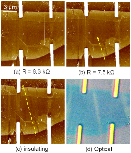
We first demonstrate that LAO can be used to electrically isolate different regions in a graphene flake. Fig. 1(a) shows a test flake before patterning, with a resistance, measured from the left to the right end, of 6.3 k. A line written across half of the flake using LAO results in a small increase of that resistance to 7.5 k (Fig. 1(b)). As the line is continuously cut through the whole flake in the subsequent lithography step, the resistance across the line becomes infinite (Fig. 1(c)). The line is barely seen in the AFM image but is clearly seen under the optical microscope (Fig. 1d). The width of the line from the optical image is overestimated by a factor of 5.
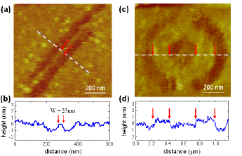
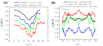
Several graphene nanodevices have been fabricated using the LAO technique. In Fig 2a we show a graphene nanoribbon formed between two LAO-patterned trenches. The width of a 800 nm long ribbon is 25 nm, the trench depth is equal to the flake thickness of 1 nm (corresponding to 1-2 layers of graphene). In Fig 2c, a ring pattern fabricated by LAO is shown. The inner and outer radii of the ring are 160 nm and 380 nm respectively. The width of the conducting region of the ring is 220 nm. We have characterized the conductance () of the ring (additional trenches were cut to confine the current in the flake to flow through the ring). At temperature () below 50 K, we observe reproducible fluctuations of conductance as a function of magnetic field () or gate voltage (), shown in Fig. 3. We attribute these fluctuations to universal conductance fluctuations (UCF) Staley et al. (2008); Graf et al. (2007); Moriki et al. (2007); Russo et al. (2008) in such a mesoscopic device. From the UCF in we estimate a phase coherence length via , where is the half with of the autocorrelation function of (after subtracting a smooth background in ) and is a flux quantum. At 4.2 K, thus calculated nm is much smaller than the circumference (1.7 m) of the ring, consistent with the absence of Aharonov-Bohm oscillations Russo et al. (2008); Recher et al. (2007) in our device.
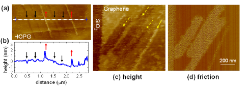
The formation of trenches as described above can be understood as due to the oxidation of graphene into volatile carbon oxides under the AFM tip Kondo et al. (1995). On the other hand, we have found that for certain LAO conditions we can form bumps rather than trenches on graphene flakes as well as on HOPG. The conditions that result in trenches or bumps can be controlled by the combination of a set point voltage (which controls the tip-sample distance in the dynamical mode) and tip bias voltage. In general, lower bias voltages and/or lower set points () result in bumps, while higher bias voltages and/or higher set points result in trenches. In Fig. 4a, 6 lines (from left to right) are written with the same tip voltage of V while was cycled through 0.3, 0.2, 0.1, 0.3, 0.2, 0.1 volts, which correspond to 15%, 10%, 5%, 15%, 10% and 5% of the free-oscillation amplitude for an unloaded tip respectively. While higher and 0.2 V consistently results in formation of trenches, bumps are written for V. Alternatively, the type of writing can be controlled by the tip bias voltage. In Fig. 4b all the lines are written with the same V while the tip bias voltage varied between -20 and -18 V for the lines marked by dashed arrows (left to right) and -16 V for the rightmost line marked with the solid arrow. This rightmost line is a bump rather than a trench. All the lines have similar morphology and are indistinguishable in a frictional image (Fig. 4c). We speculate that at low bias voltages and low set point voltages, the AFM tip partially oxidize the graphene into nonvolatile graphene oxide (GO) with some oxygen incorporated into the graphene lattice. GO is known to have a larger layer thickness Gómez-Navarro et al. (2007) than graphene, therefore corresponding to bumps on graphene or graphite surfaces.
To summarize, we have demonstrated AFM-based LAO on graphene. The lithography is capable of producing small features ( nm) with sub-nm spacial resolution, allowing in situ monitoring of the device parameters (such as dimensions or electrical conduction) during the fabrication and easy tuning of the fabrication. We also found that we can write either trenches or bumps on the graphene surface depending on the lithography conditions. We attribute bumps to partial oxidation of the graphene with oxygen incorporated into the graphene lattice.
The work was partially supported by NSF Grant No. ECS-0348289. YPC gratefully acknowledge the support by the Nanoelectronics Research Initiative (NRI) through the Midwest Institute of Nanoelectronics Discovery (MIND) and by the Miller Family endowment.
References
- Novoselov et al. (2004) K. Novoselov, A. Geim, S. Morozov, D. Jiang, Y. Zhang, S. Dubonos, I. Grigorieva, and A. Firsov, Science 306, 666 (2004).
- Zhang et al. (2005) Y. Zhang, Y.-W. Tan, H. L. Stormer, and P. Kim, Nature 438, 201 (2005).
- Novoselov et al. (2005) K. Novoselov, A. Geim, S. Morozov, D. Jiang, M. Katsnelson, I. Grigorieva, S. Dubonos, and A. Firsov, Nature 438, 197 (2005).
- Berger et al. (2006) C. Berger, Z. Song, X. Li, X. Wu, N. Brown, C. Naud, D. Mayou, T. Li, J. Hass, A. N. Marchenkov, et al., Science 312, 1191 (2006).
- Novoselov et al. (2007) K. Novoselov, Z. Jiang, Y. Zhang, S. Morozov, H. L. Stormer, U. Zeitler, J. Maan, G. Boebinger, P. Kim, and A. Geim, Science 315, 1379 (2007).
- Geim and Novoselov (2007) A. K. Geim and K. S. Novoselov, Nature Mater. 6, 183 (2007).
- Russo et al. (2008) S. Russo, J. B. Oostinga, D. Wehenkel, H. B. Heersche, S. S. Sobhani, L. M. K. Vandersypen, and A. F. Morpurgo, Phys. Rev. B 77, 085413 (2008).
- Han et al. (2007) M. Y. Han, B. Oezyilmaz, Y. Zhang, and P. Kim, Phys. Rev. Lett. 98, 206805 (2007).
- Chen et al. (2007) Z. Chen, Y.-M. Lin, M. J. Rooks, and P. Avouris, Phys. E 40, 228 (2007).
- Bunch et al. (2005) J. S. Bunch, Y. Yaish, M. Brink, K. Bolotin, and P. L. McEuen, Nano Lett. 5, 287 (2005).
- Stampfer et al. (2008) C. Stampfer, J. Guettinger, F. Molitor, D. Graf, T. Ihn, and K. Ensslin, Appl. Phys. Lett. 92, 012102 (2008).
- Tseng et al. (2005) A. A. Tseng, A. Notargiacomo, and T. P. Chen, J Vac. Sci. Tech. B 23, 877 (2005).
- Snow and Campbell (1994) E. S. Snow and P. M. Campbell, Appl. Phys. Lett. 64, 1932 (1994).
- Held et al. (1997) R. Held, T. Heinzel, A. P. Studerus, K. Ensslin, and M. Holland, Appl. Phys. Lett. 71, 2689 (1997).
- Rokhinson et al. (2002) L. P. Rokhinson, D. C. Tsui, L. N. Pfeiffer, and K. W. West, Superlattices Microstruct. 32, 99 (2002).
- Kim et al. (2003) D. H. Kim, J. Y. Koo, and J. J. Kim, Phys. Rev. B 68, 113406 (2003).
- Park et al. (2007) J. G. Park, C. Zhang, R. Liang, and B. Wang, Nanotechnology 18, 405306 (2007).
- Staley et al. (2008) N. Staley, C. Puls, and Y. Liu, Phys. Rev. B 77, 155429 (2008).
- Graf et al. (2007) D. Graf, F. Molitor, T.Ihn, and K. Ensslin, Phys. Rev. B 75, 245429 (2007).
- Moriki et al. (2007) T. Moriki, A. Kanda, T. Sato, H. Miyazaki, S. Odaka, Y. Ootuka, Y. Aoyagi, and K. Tsukagoshi, Phys. E 40, 241 (2007).
- Recher et al. (2007) P. Recher, B. Trauzettel, A. Rycerz, Y. M. Blanter, C. W. J. Beenakker, and A. F. Morpurgo, Phys. Rev. B 76, 235404 (2007).
- Kondo et al. (1995) S. Kondo, S. Heike, M. Lutwyche, and Y. Wada, J. Appl. Phys. 78, 155 (1995).
- Gómez-Navarro et al. (2007) C. Gómez-Navarro, R. T. Weitz, A. M. Bittner, M. Scolari, A. Mews, M. Burghard, and K. Kern, Nano Lett. 7, 3499 (2007).