Electronic structures of organic molecule encapsulated BN nanotubes under transverse electric field
Abstract
The electronic structures of boron nitride nanotubes (BNNTs) doped by different organic molecules under a transverse electric field were investigated via first-principles calculations. The external field reduces the energy gap of BNNT, thus makes the molecular bands closer to the BNNT band edges and enhances the charge transfers between BNNT and molecules. The effects of the electric field direction on the band structure are negligible. The electric field shielding effect of BNNT to the inside organic molecules is discussed. Organic molecule doping strongly modifies the optical property of BNNT, and the absorption edge is red-shifted under static transverse electric field.
pacs:
75.75.+a, 73.22.-f, 72.80.RjI introduction
Nanotube is a very important actor in nanodevice applications due to its novel properties. Compared to the more widely studied carbon nanotube (CNT), boron nitride nanotube (BNNT) has its own distinctive properties. Besides the excellent mechanical stiffness and thermal conductivity comparable to CNT, review BNNT has a unified electronic structure regardless of its diameter, chirality, and the number of walls of the tube. bn1 ; bn2 ; bn3 BNNT also shows pronounced resistance to oxidation, and it is stable up to 700 ∘C in air, while CNT survives only below 400 ∘C. bn5 All these properties make BNNT an attractive candidate for nano-electronics.
Pristine BNNT is a wide-gap semiconductor. For electronics application, it is desirable to make - or -type doping to BNNT. Our previous study shows that the electronic structure of BNNT can be modified by organic molecule encapsulation. bnhe Electrophilic molecule introduces acceptor states in the wide gap of BNNT close to the valence band edge (VBE), which makes the doped system a -type semiconductor. However, with typical nucleophilic organic molecules, instead of shallow donor states, only deep occupied molecular states are observed. There is a significant electron transfer from BNNT to an electrophilic molecule, while the charge transfer between a nucleophilic molecule and BNNT is negligible.
On the other hand, previous theoretical studies field0 ; field1 ; field2 showed that the band gap of CNT or BNNT can be reduced and even closed by applying a transverse electric field, due to the giant Stark effect (GSE). field1 The electric field can mix the nearby subband states in the valence band (VB) complex and conduction band (CB) complex separately, leading to an electric field dependence for the band gap. This effect is more remarkable in BNNTs than in CNTs, due to the reduced screening of the electric field in BNNTs. The GSE was lately confirmed experimentally using the bias dependent scanning tunneling microscopy and scanning tunneling spectroscopy. field3
Since the electronic structure of BNNT can be tuned by both organic molecule encapsulation and transverse electric field, it is thus interesting to see what will happen if we apply both. In this paper, by performing density functional theory (DFT) calculations, we study the electronic structures of organic molecule encapsulated BNNTs under a transverse electric field. The electrostatic shielding of BNNT to the inside molecules and the effects of organic molecule doping and electric field on the optical properties of BNNT are also studied.
Following our previous study, bnhe several typical electrophilic and nucleophilic molecules are considered for BNNT encapsulation. The two electrophilic molecules studied are tetracyano-p-quinodimethane (TCNQ) and tetrafluorocyano-p-quinodimethane (F4TQ). Three nucleophilic molecules are selected: tetrakis(dimethylamino)ethylene (TDAE), anthracene (ANTR), and tetrathia-fulvalene (TTF). The (16,0) BNNT is chosen as a prototype in this study. We name the organic molecules capsulated BNNT as M@BN, where M is the name of the doped organic molecules.

The rest of the paper is organized as follows: In Sec. II, the theoretical approach and computational details are briefly described. In Sec. III, the calculated band structures, charge transfers between BNNT and molecules, shielding effect under electric field, and optical properties are discussed. Finally, we conclude in Sec. IV.
II Computational Details
To investigate the geometry structure and electronic states of the organic molecule encapsulated BNNT, we performed first-principles spin-polarized DFT calculations. The computational details of geometry optimization and band structure calculation can be found in our previous study, bnhe and we only give a brief summary here. We used the projector augmented-wave (PAW) method 20 ; 21 implemented in the Vienna Ab Initio Simulation Package (VASP). 17 ; 18 The Perdew, Burke and Ernzerhof (PBE) exchange-correlation functional was chosen. 19 We note that more rigorous band structure calculations are required to yield correct band gaps. Baumeier07 However, PBE functional has been widely used in similar systems, and it should give correct trends which are interested in this study. The energy cutoff for plane-waves was 400 eV. In our calculation, each BNNT was separated by 10 Å of vacuum, and the minimum distance between periodically repeated organic molecules along the BNNT tube axis was 8.7Å. A 411 -centered Monhkorst-Pack -point grid was used for Brillouin zone sampling.
The way to handle electric field in VASP is adding an artificial dipole sheet in the middle of the vacuum part in the periodic supercell. vaspdipole1 ; vaspdipole2 In our study, the direction of the electric field was chosen to be perpendicular to the nanotube’s axis (along the direction), with a magnitude of 0.20 or 0.50 V/Å. As discussed later, the selected fields are strong enough to make significant change of the electronic structure, and weak enough to avoid artificial field emission.
All linear optical properties, such as absorption coefficient and refractive index, can be obtained as functions of dielectric function. The real part of the dielectric function can be obtained from its imaginary part by Kramer-Kronig transformation, and the imaginary part can be calculated based on the independent-particle approximation, Adolph0108 i.e.,
| (1) |
where is the unit cell volume, and is the photon energy. Summations for and are performed for valence and conduction bands, respectively. denotes the dipole transition matrix elements obtained from the self-consistent band structure calculations and is the point weighting. The same method has been applied to h-BN, and the results are in reasonably good agreement with experiments. Guo0502 The number of bands used for dielectric function calculations are the sum of the electron number and the ion number. The number of occupied bands is half of the number of electron, and the number of unoccupied bands are more than 380 for all the systems studied in this paper. The optical polarization in dielectric function calculations is perpendicular to the nanotube axis. In this way, for some parts of the tube wall, the optical polarization is nearly perpendicular to the BN layer, while for the other parts of the tube wall, it is roughly parallel to the BN layer.
III RESULTS AND DISCUSSION
III.1 Geometric and band structures
As reported in our previous study, bnhe after the organic molecules are encapsulated into BNNT, their geometries changes little. This suggests the weak interaction between BNNT and the encapsulated molecules, due to the large distances between them. The separations between neighboring molecules and between molecule and BNNT are larger than additions of the corresponding atomic van der Waals radius. Optimizations under the transverse electric field gave similar structure as in the zero-field case. The optimized geometrical structures under a 0.5 V/Å electric field are shown in Fig. 1. The relaxed geometries of the M@BN systems before and after applying electric field change little. The largest change of bond length, comparing to the geometry under zero field, is smaller than 0.01 Å. Consistently, the direction of the transverse field does not affect the geometric and electronic structures. Our test calculation gave almost identical band structures for F4TQ@BN under 0.5 V/Å transverse electric field along two different directions. For simplicity, in the rest part of the paper, all electronic structure calculations were done based on the geometrical structures obtained without electric field.
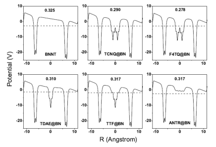
Before calculating the electronic structure of M@BN with transverse electric field applied, two important issues are needed to be discussed. One is that the vacuum region should be broad enough to avoid the overlap between the charge density and the artificial dipole sheet used to generate electric field. The width of the vacuum layer between two neighboring BNNTs in our calculation is 10 Å, and the work function of (16,0) BNNT is 6.36 eV. The charge density of BNNT roughly decay as , where is the work function in eV and is the distance from the BNNT in Å. vaspdipole3 The charge density thus decays one magnitude every 0.91 Å. The dipole sheet is 5 Å far from the BNNT, and there is thus only negligible charge density there. The other issue is that the vacuum region should not be too broad so as to attract electrons to vacuum (field emission). In Fig. 2, we plot the electrostatic potential of the M@BN system under a 0.5 V/Å electric field, the strongest electric field used in our calculations. We can see that the lowest potential in vacuum region is still higher than the edge of the highest occupied band (HOBand), which confirms that the artificial field emission has not been introduced in this study.
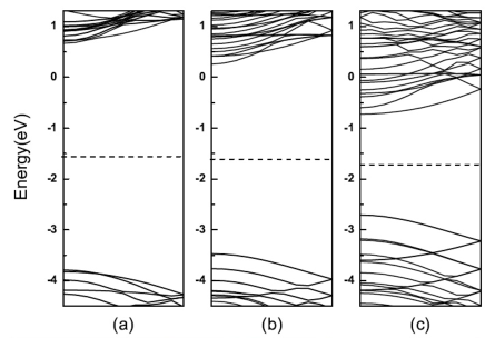
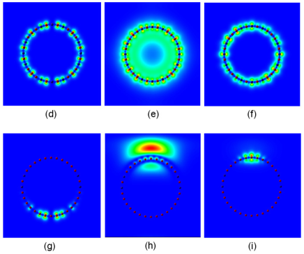
We first calculate the band structure of the pristine BNNT under the 0.2 and 0.5 V/Å electric fields, and the results are shown in Fig. 3. The band gap decreases from 4.45 to 3.73 and 1.98 eV, when the field increases from 0 to 0.2 and 0.5 V/Å, respectively. Our result is consistent with the previous theoretical study on similar systems. field1 Such band gap decrease is a result of the extensive mixing among the subband states within the valence and conduction band complex under electric filed. The band mixing is also reflected by the band-resolved charge density distributions, as shown in Fig. 3, where the density of the HOBand, the lowest unoccupied band (LUBand), and LUBand+1 under 0.0 and 0.5 V/Å field are plotted. The orbital density move along the electric field for occupied states, and against the field direction for unoccupied states. From the density distributions, the LUBand state can be identified as a nearly free electron (NFE) state. field1
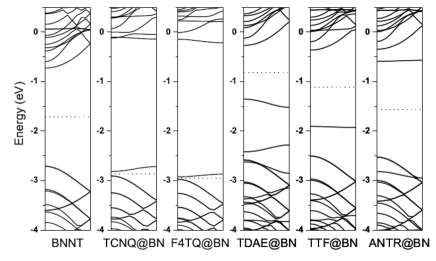
The band structures of the M@BN systems under 0.2 and 0.5 V/Å electric field are then calculated. Similar to results under zero electric field, bnhe the bands are either mainly from molecules or mainly from BNNT. The molecular bands are much flatter than the BNNT bands. Since there is no qualitative difference between the band structure of the M@BN systems under 0.2 and 0.5 V/Å electric fields, we will focus on the 0.5 V/Å case (Fig. 4). For the two electrophilic molecules (TCNQ and F4TQ), the lowest unoccupied molecular bands become very close to the BNNT VBE, which means good -type doping. It also suggests a considerable charge transfer between the molecules and the BNNT. We define the gap between the lowest unoccupied molecular band and the BNNT VBE as , and the gap between the highest occupied molecular band and the BNNT conduction band edge (CBE) as . Their values are listed in Table 1. For the nucleophilic organic molecules TDAE and TTF, drops from 2.30 and 2.85 eV at zero field bnhe to 1.08 and 1.54 eV, respectively. However, it is still too large to form good -type doping. For ANTR@BN, the highest occupied molecular band is pushed into the BNNT valence band manifest, and there is only an unoccupied molecular band close to the BNNT CBE. Therefore, neither -type or -type doping is introduced to BNNT by ANTR encapsulation.
| Gap | BN | TCNQ | F4TQ | TDAE | TTF | ANTR | |
|---|---|---|---|---|---|---|---|
| 0.0 | — | 0.15 | 0.09 | 4.37 | 3.55 | 2.96 | |
| 0.2 | — | 0.17 | 0.11 | — | 3.25 | 2.65 | |
| 0.5 | — | 0.09 | 0.05 | — | — | 1.93 | |
| 0.0 | — | — | — | 2.30 | 2.85 | 3.71 | |
| 0.2 | — | — | — | 1.86 | 2.49 | 3.40 | |
| 0.5 | — | — | — | 1.08 | 1.54 | — | |
| 0.0 | 4.45 | 4.45 | 4.48 | 4.45 | 4.46 | 4.43 | |
| 0.2 | 3.73 | 4.00 | 4.18 | 3.63 | 3.79 | 3.81 | |
| 0.5 | 1.98 | 2.79 | 2.91 | 2.31 | 2.14 | 2.18 |
To consider the molecular effect on the intrinsic electronic structure of BNNT under electric field, we define the energy gap between the CBE and VBE of BNNT as . As shown in Table 1, without external field, it is not very sensitive to the type of molecules. However, for TCNQ@BN and F4TQ@BN under electric field is much larger than other systems under the same field. This can be easily understood by their electronic structures. Under strong external field, the energy gaps of TCNQ@BN and F4TQ@BN become very small, which means enhanced metallicity and stronger electrostatic screening. With stronger screening, the reduction of electrostatic potential along the direction of electric field is slower (see Fig. 2), therefore, reduction compared to pristine BNNT and other M@BN systems is smaller. Similar behavior has been observed in our study on defective BNNTs under an electric field. bnhu
III.2 Charge transfer
An important property of the molecule encapsulated system is the charge transfer between the molecules and BNNT. We calculate the charge transfer using the method described in our previous work, bnhe originally proposed by Lu et al..charge1 Briefly speaking, the boundary between the organic molecule and the BNNT is determined by the maximum/minimum position of the cylinder-integrated differential electron density curve, and the corresponding maximum/minimum value is the charge transfer value. The differential electron density is defined as the difference between electron densities of the M@BN system under electric field and the sum of charge densities of BNNT and molecules without electric field. The range of the radial position of boundary between molecule and BNNT can be estimated by the density distribution of the BNNT bands. For electrophilic molecules, should be inside the region where the BNNT HOBand has a high density ( Å), while for nucleophilic molecules, should be inside region where the BNNT LUBand has a high density ( Å). bnhe
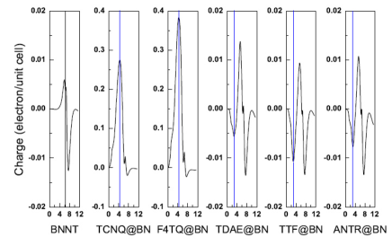
For pristine BNNT, the differential electron density is just the density change before and after applying electric field. As shown in Fig. 5, the electron density increases inside the nanotube wall, while it decrease outside the wall. Of course, the absolute value of this change is very small (0.01 electron). For the electrophilic organic molecules TCNQ and F4TQ, under 0.5 V/Å electric field, there are 0.28 and 0.38 electrons per molecule transfer from BNNT, about twice as the value without field (0.10 and 0.24 electron). bnhe This is due to the closer molecular state in energy to VBE. The boundary radius is 4.3 Å, which is basically the midpoint between the molecule and the BNNT as in the no field case. For the nucleophilic organic molecules TDAE, TTF and ANTR, the charge transfers form molecules to BN also increase, which is 0.006, 0.011, and 0.008 electron per molecule, respectively (0.004, 0.008, and 0.005 electrons without external field). Such small electron transfers also indicate that the doped system is not a good -type semiconductor.
III.3 Shielding effect
It is interesting to study the effects of BNNT to the geometry and electronic structure of the inside molecules under an electric field. In Fig. 6, we compare the molecular partial densities of states (PDOS) with and without external field for two representative molecules: an electrophilic one (F4TQ) and a nucleophilic one (TTF). The calculated PDOS shows different behaviors for these two types of molecules. For the electrophilic organic molecules F4TQ (Fig. 6a), there is an nearly rigid upshift of the molecular PDOS after applying the electric field. This is due to the electron transfer from BNNT to the molecules. For the nucleophilic organic molecules TTF (Fig. 6c), the molecular PDOS almost does not change after applying the electric field, which is consistent with the little charge transfers between BNNT and the molecules.
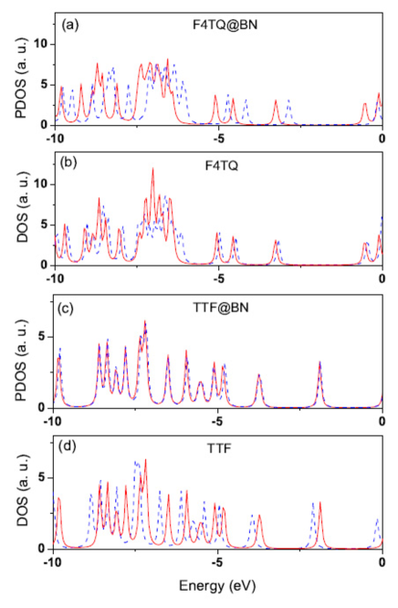
We also check the shielding effect by applying electric field to individual molecules without a BNNT encapsulation. First, we relax the geometry of the individual molecules under the 0.5 V/Å electric field. Contrasting to the encapsulated case, we found a significant geometry relaxation after applying the electric field. Then, we fix the molecular geometry to the one as inside BNNT, and calculate the electronic structure under zero and finite electric field. The effect of electric field to the molecular electronic structures for individual molecules is different from that for molecules encapsulated by BNNT (see Fig. 6). For F4TQ molecule, the DOS energy shift caused by electric field is smaller than that for PDOS of F4TQ@BN. However, we can see a notable change of the overall DOS shape after applying the electric field. For TTF, electric field shifts the DOS of individual molecules, but it does not change the molecular PDOS. In summary, our results indicates, although not good as CNT, the BNNT still provides a significant electrostatic shielding for the inside molecules: the geometry of the inside molecules and the electronic structures of nucleophilic molecules are almost not affected by an external field under the protection of BNNT.
III.4 Optical properties
The calculated imaginary part of the dielectric function of the pristine BNNT without external electric field is shown in the inset of Fig. 7a. A much denser -point sampling is required to obtain smooth curves. Guo0502 However, the main features of are already presented in our results. And our calculated of prinstine BNNT agrees well with the previous theoretical result on the zigzag BNNTs. Guo0502 Mainly, there are three peaks at about 5.6, 10.6, and 13.5 eV, respectively. The strong peak around 5.6 eV corresponds to the interband transitions. The two other peaks higher in energy and weaker in intensity are associated with interband transitions also involving the bands. We note that the peak around 10.6 eV does not appear in our test calculation with the optical polarization along the tube axis. By optical selection rule analysis, Guo0502 the 10.6 eV peak should correspond to and transitions, and the 13.5 peak mainly contributed by transitions. In Fig. 7a, we also plot of the pristine BNNT under transverse electric field. Similar to a previous study on pristine BNNT, field5 the whole imaginary dielectric function is not strongly affected by the static field, but the absorption edge is red-shifted.
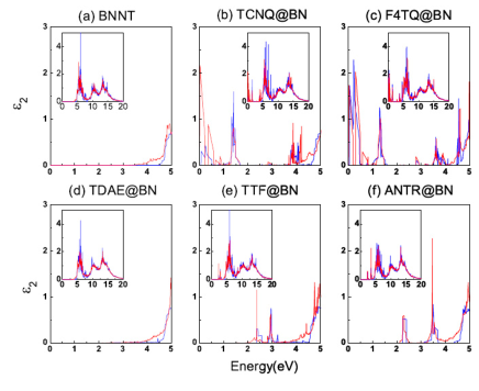
With molecule intercalation, all the three peaks are still clearly shown in the M@BN system. However, new features appear in the low-energy region from 0 to 5 eV. These peaks below the BNNT absorption edge (4.5 eV) are clearly from transitions between molecular bands and the BNNT bands or between molecular bands themselves. For the two electrophilic molecules, there are peaks close to the zero energy. This is consistent with the very narrow band gap calculated for these two systems. There is no significant peaks below 4.5 eV for TDAE@BN, and the new peaks for TTF@BN and ANTR@BN are close to the BNNT absorption edge. Our results indicate that the optical property of BNNT can be strongly modified by different organic molecule encapsulation.
Next, we study the case where both molecule intercalation and electric field exist. The theoretical imaginary part of the dielectric functions of the molecule doped BNNT under a 0.5 V/Å transverse static electric field are also presented in Fig. 7. The three peaks from BNNT are still not strongly affected by the static field. However, if we look into the details below 5 eV, we can see three different behaviors. For transitions between valence band and conductance bands of BNNT, the electric field GSE broadens the band manifests, thus broadens the absorption peaks too. This broadening effect red-shifts the absorption edge of BNNT as shown in Fig. 7d. For transitions between molecular bands, due to electrostatic shielding of BNNT, the electric field does not strongly affect the peaks, as shown in Fig. 7e and 7f. For transitions between BNNT bands and molecular bands, the electric field affects both the amplitude of the peaks and the peak positions, as shown in Fig. 7b and 7c.
IV conclusion
In summary, we calculate the electronic structure and optical properties of BNNT under transverse electric field with different molecule intercalations. When applying transverse electric field, the band gap of BNNT decrease, while the band structures of organic molecules change little, or only with a rigid shift. After applying electric field, there is more charge transfer between molecules and nanotube in the -type semiconductors TCNQ@BN and F4TQ@BN. BNNT provides relatively good electrostatic shielding for the geometry relaxation of the inside organic molecular chain, and for the electronic structure of nucleophilic molecules. Organic molecule doping strongly modifies the optical properties of the composite M@BN systems. The absorption edge is slightly red-shifted under static electric field.
Acknowledgements.
The postprocessing routine downloaded from the homepage of Prof. Furthmuller has been used in the optical property calculations. This work is partially supported by the National Natural Science Foundation of China (50721091, 20533030, 50731160010), by National Key Basic Research Program under Grant No.2006CB922004, by the USTC-HP HPC project, and by the SCCAS and Shanghai Supercomputer Center.References
- (1) D. Golberg, Y. Bando, C. C. Tang, and C. Y. Zhi, Adv. Mater. 19, 2413(2007).
- (2) A. Rubio, J. L. Corkill, and M. L. Cohen, Phys. Rev. B 49, 5081 (1994).
- (3) N. G. Chopra, R. J. Luyken, K. Cherrey, V. H. Crespi, M. L. Cohen, S. G. Louie, and A. Zettl, Science 269, 966 (1995).
- (4) X. Blase, A. Rubio, S. G. Louie, and M. L. Cohen, Europhy. Lett. 28, 335 (1994).
- (5) Y. Chen, J. Zou, S. J. Campbell, and G. L. Caer, Appl. Phys. Lett. 84, 2430 (2004).
- (6) W. He, Z. Li, J. Yang, and J. G. Hou, J. Chem. Phys., 128, 164701 (2008).
- (7) J. O’Keeffe, C. Wei, and K. Cho, Appl. Phys. Lett. 80, 676 (2002).
- (8) K. H. Khoo, M. S. C. Mazzoni, and S. G. Louie, Phys, Rev. B 69, 201401 (2004)
- (9) C. W. Chen, M. H. Lee, adn S. J. Clark, Nanotechnology 15, 1837 (2004)
- (10) M. Ishigami, J. D. Sau, S. Aloni, M. L. Cohen, and A. Zettl, Phys, Rev. Lett. 94, 056804 (2005)
- (11) G. Kresse, D. Joubert, Phys. Rev. B 59, 1758 (1999).
- (12) P. E. Blochl, Phys. Rev. 50, 17953 (1994).
- (13) G. Kresse, J. Furthm ller, Phys. Rev. B 64, 11169 (1996).
- (14) G. Kresse, J. Furthmuller, Comput. Mater. Sci. 6, 15 (1996).
- (15) J. P. Perdew, K. Burke, and M. Ernzerhof, Phys. Rev. Lett. 77, 3865 (1996).
- (16) B. Baumeier, P. Kruger, and J. Pollmann, Phys. Rev. B 76, 085407 (2007).
- (17) J. Neugebauer and M. Scheffler, Phys. Rev. B 46, 16067 (1992).
- (18) G. Kresse and J. Furthmuller, VASP Guide.
- (19) B. Adolph, J. Furthmuller, and F. Bechsted, Phys. Rev. B 63, 125108 (2001)
- (20) G. Y. Guo and J. C. Lin, Phys. Rev. B 71, 165402 (2005)
- (21) P. J. Feibelman, Phys. Rev. B 64, 125403(2001).
- (22) S. Hu, Z. Li, X. C. Zeng, and J. Yang, J. Phys. Chem. C, ASAP article (2008)
- (23) X. Lu, M. Grobis, K. H. Khoo, S. G. Louie, and M. F. Crommie, Phys. Rev. B 70, 115418 (2004).
- (24) C. W. Chen, M. H. Lee, and Y. T. Lin, Appl. Phys. Lett. 89, 223105 (2006).