Adsorption of metal impurities on H-terminated Si surfaces and their influence on the wet chemical etching of Si
Abstract
We use first-principles methods to investigate the adsorption of Cu, Pb, Ag, and Mg onto a H-terminated Si surface. We show that Cu and Pb can adsorb strongly while Ag and Mg are fairly inert. In addition, two types of adsorption states are seen to exist for Pb. We also study the clustering energetics of Cu and Pb on the surface and find that while Cu clusters eagerly, Pb may prefer to form only small clusters of a few atoms. This kind of behavior of impurities is incorporated in kinetic Monte Carlo simulations of wet etching of Si. The simulation results agree with experiments supporting the idea that micromasking by Cu clusters and Pb atoms is the mechanism through which these impurities affect the etching process.
pacs:
81.65.Cf, 68.43.-hKeywords: adsorption, silicon, metal impurities, clusters, etching, pinning, surface morphology, ab-initio, kinetic Monte Carlo
1 Introduction
Anisotropic wet chemical etching of silicon is an important method in the fabrication of micro-electromechanics systems (MEMS) such as cantilevers [1], microfluidic channels [2], and inertial sensors [3]. However, as structures become smaller, possible defects and rough features can become detrimental for the manufactured devices. Therefore it is important to understand how the features seen on etched surfaces are created. In principle, the etching process should rapidly attack protrusions and lead to atomistically smooth surfaces [4]. Still, impurities [5, 6, 7], hydrogen bubbles [8, 5, 9] or etchant inhomogeneities [10, 11] can disturb the process and lead to features such as hillocks [5, 12, 13, 14], zig-zags [15, 16], pits [7] or step bunches [4, 17, 11]. Since these morphologies are the result of complicated interplay between the etchant, the surface, and the possible impurities, the problem of rough surfaces is also theoretically challenging.
Experimentally, it is known that out of the metal impurities commonly present in etchant solutions, only Cu and Pb affect the etching process [6, 18, 7] while the presence of metals such as Ag, Al, Cr, Zn, Ni, Fe, and Mg has no effect [19] (Mg can nullify the effects of Cu if both are present in the etchant, though [20]). In general, having Cu in the etchant results in rough surfaces and sometimes also in low etch rates. For instance, on the (110) and (100) surfaces, Cu can induce the appearance of hillocks or etch pits [7]. Pb only affects the etch rates without changing the surface morphologies. In the case of Cu, this behavior is understood to be due to adsorption of the impurity particles on the surface. Adsorption enables the Cu to locally inhibit etching and act as a pinning agent [7, 19]. The Si surface is nearly fully terminated by Si–H bonds during wet etching [21, 22, 4] and first-principles calculations have shown that Cu adsorption on such a surface is energetically favored [23]. Furthermore, Monte Carlo simulations incorporating adsorbing impurities have demonstrated that local pinning by impurities and impurity clusters can change the morphology of etched surfaces [14, 24]. However, a comprehensive theoretical understanding of the influence of other metal impurities does not exist.
In order to form a complete picture of the behavior of metal impurities in wet etching of Si, we investigate the adsorption of Pb, Ag, and Mg in addition to Cu. (Note that the adsorption energies of individual copper atoms cited in this article have been presented previously in [23].) While Cu and Pb are the most active metals according to the existing experimental knowledge, Ag and Mg are also examined as examples of the other, inert impurities. We use first-principles calculations to study the adsorption energetics of these impurities on the hydrogen-terminated Si surface. For Cu and Pb, we also investigate the tendency for forming clusters on the surface. Based on the first-principles data, we carry out kinetic Monte Carlo simulations of etching under the influence of different types of impurities. By comparing the resulting surface morphologies and roughnesses as well as etch rates to real etched surfaces, we link the theoretical study to experiments.
2 Methods
2.1 First-principles calculations
We calculate the adsorption energies of Cu, Pb, Mg and Ag atoms on H-terminated Si surfaces at various surface sites using the linear combination of atomic orbitals based siesta code [25, 26] implementing the density-functional theory (DFT) [27, 28]. For exchange-correlation, we use the PBE gradient corrected functional [29]. Core electrons are described by norm-conserving pseudopotentials using the Troullier-Martins parametrization and including scalar relativistic corrections. The pseudopotentials were generated in electron configurations [Ne] for Si, for H, [Ar] for Cu, [Xe] for Pb, [Ne] for Mg, and [Kr] for Ag. Here square brackets denote the core electron part. Having tested different basis sets, we use double zeta with a single shell of polarization orbitals for Si, H, and the electrons of Ag and triple zeta with two shells of polarization for Cu, Pb, Mg, and the electrons of Ag. The convergence of system properties with respect to points and mesh was also checked. A () Monkhorst-Pack -mesh and an energy cutoff of 150 Ry were found sufficient for these systems. The used energy shift is 25 meV. Basis set superposition errors are handled using counterpoise corrections [30]. The metal impurities are treated as neutral atoms in the calculations. The impurities present in an etchant are originally in an ionic form in the solution, however, the ions are reduced at the surface and adsorb in the neutral state [23, 6, 7].
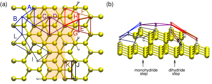
The calculations are carried out in supercells of 79–113 atoms forming two-dimensional Si slabs with both sides terminated by H atoms in order to saturate dangling bonds. The convergence with respect to slab thickness was tested and three or four layers of Si atoms were found to be sufficient. The bottom layer of hydrogen and the lowest layer of silicon are kept frozen, mimicking bulk silicon. Other atoms are allowed to relax using a conjugate gradient scheme until atomic forces become 0.02 eV/Å or less. The surface orientations of the slabs used in the calculations are (111), (112) and (221). This allows us to probe the adsorption energies of impurities at a variety of sites on both ideal (111) terraces as well as on stepped or kinked surfaces. The most important site types that appear on realistic surfaces are shown in Figure 1 using the naming conventions of [23, 24]. (The image does not represent a calculation supercell.) Note that two kinds of steps are shown in the image. The Si in the step on the left share a bond with one H while on the right there are two H-saturated bonds per Si. These step types are called mono- and dihydride steps and they appear on the (221) and (112) surfaces, respectively.
2.2 Kinetic Monte Carlo simulations
We model the etching process using an atomistic kinetic Monte Carlo (KMC) approach. The possible events in the simulation are Si removal, Cu/Pb adsorption, and Cu/Pb desorption and at each KMC step the simulator stochastically decides between these according to their relative occurrence rates. Our implementation [31, 19] uses the K-level search algorithm [32, 33] and an event-tree which combines both Si etching and impurity adsorption and desorption [24]. The Si are treated as an ideal lattice where the removal rates for all atoms are determined by their local neighborhoods, i.e., the numbers of the first and second nearest neighbor Si atoms on surface and in bulk [34]. The relative removal rates for the most common sites are given in Table LABEL:table:rates. A more thorough classification of the Si atom types on the surface as categorized by the simulator is given in [35]. Low etchant concentration is realized in simulations by setting the etch rate of dihydride steps much higher than that of monohydride steps. Similarly, high concentration corresponds to rapidly etching monohydride steps [19].
-
low concentration high concentration terrace monohydride step monohydride kink monohydride double kink dihydride step dihydride kink dihydride double kink
The surface is characterized by a constantly updated triangulation mesh based on the positions of H atoms on the surface. This mesh is generated as a Delaunay triangulation [36] from a 2D projection of the atomic positions. Each triangle in the mesh then represents a potential adsorption site for an impurity in the simulation. The triangles are identified according to their shapes and unique adsorption and desorption rates are assigned to each triangle type. The rates are estimated as , where is the activation energy, is a parameter, and is the temperature (350 K) multiplied by the Boltzmann constant. The adsorption rates of Cu are site-dependent and the used activation energy values reach from 0.1 to 1.5 eV [24]. The adsorption rates for Pb are treated site-independently with an activation energy of 0.3 eV for all triangles (see Subsection 3.1). The etchant is treated as a limited reservoir of impurities which may adsorb on the surface. Once adsorbed, an impurity pins the Si atoms connected to the adsorption site triangle. In this model pinning is handled by lowering the removal rates of the silicons by a factor of . Desorption of impurities can occur thermally with an activation energy of 1.5 eV or via underetching, i.e., by removing a Si to which the impurity is connected [24].
To simulate impurity clustering in a simplified way, the adsorption rates on sites (triangles) sharing a vertex with the already impurity-populated sites are multiplied by an enhancement factor. We use a factor of , where eV for Cu and eV (i.e. no clustering) for Pb, as explained in Subsection 3.2. For a more detailed description of the simulation method and especially the treatment of Cu clusters, see [24] (the “Interaction enhanced adsorption” scheme).
3 Results
3.1 Adsorption of individual impurities
The calculated adsorption energies for the different metal impurities on various surface sites are given in Table LABEL:table:ae. Since we know from experiments that only Cu and Pb affect the etching process, most effort has been allocated for studying these metals. Two values have been calculated also for Mg and Ag for comparison.
-
site Cu Pb (A) Pb (R) Mg Ag A * - - B * - - C * D * - - E * - - F - * G * - - H - * - - I - * - - J - * - - K - * - -
The results for Cu have been previously presented and analyzed in detail in [23]. In summary, adsorption of Cu is energetically favorable, with the site-dependent adsorption energies being approximately proportional to the number of bonds the Cu atoms can create with the surface H and Si. The adsorbed Cu atoms typically sit in between H atoms in the middle of the triangular or quadrangular sites drawn in Figure 1. The highest adsorption energy (in absolute value), 1.43 eV, is on the F site found on vertical dihydride steps. Also the H and I sites found on dihydride steps and kinks, respectively, are favored by Cu.
For Pb, we find two qualitatively different adsorption states. As an example, electron density plots of these states at the G site are shown in Figure 2. Like Cu, Pb can adsorb on the H-terminated surface. However, the bonding between Pb and H atoms is weak and the adsorption energies are lower than for Cu [column “Pb (A)” in Table LABEL:table:ae]. Additionally, Pb does not exhibit strong site specificity like Cu does — adsorption energies are close to 0.5 eV regardless of the adsorption site. The lowest energy found is 0.39 eV for the terrace site D, and the highest is 0.54 eV for the dihydride step site G shown in Figure 2 (a).
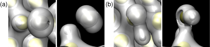
The other possibility, shown in Figure 2 (b), is that a Pb replaces a hydrogen on the surface in a reaction Si–H + Pb Si–Pb–H. The energy gain in this reaction is always higher than in plain adsorption of Pb or Cu [column “Pb (R)” in Table LABEL:table:ae] and the reaction can happen on any site. The energy change when replacing the H atom on a monohydride step (corresponds to the shared vertex for sites A and B in Figure 1) is 1.22 eV. (The other vertices of the A and B triangles in Figure 1 are not equivalent, but reactions where Hs at these sites are replaced have not been calculated.) On the (111) terrace (H shared by sites C and D), the energy is 1.26 eV. However, on these sites, merely placing a Pb on the site and letting the geometry relax results in the weakly adsorbed state. (This is denoted by asterisks in Table LABEL:table:ae.) The reacted states are reached from initial configurations where one hydrogen atom is slightly pulled away from the surface allowing the Pb to bond between Si and H.
On the dihydride step, a few different configurations are found depending on the initial position from which the Pb atom is allowed to relax. Placing a Pb on the G site results in a reaction with the hydrogen on the upper terrace near the step (H shared by sites D and G) with an energy of 1.64 eV. The resulting structure is shown in Figure 2 (b). (In this case the weakly adsorbed state is reached by placing the Pb initially relatively far away from the surface.) Starting from the F or H sites leads to a reaction with an H on the horizontal dihydride step (H shared by sites E–H), but the obtained final configurations differ in the orientation of the Si–Pb–H structure. A configuration where the hydrogen in the Pb–H pair ends up on the side of the upper terrace (relaxation of Pb started from site F) is a local minimum with an energy of 1.55 eV. The opposite case, where the hydrogen is on the side of the lower terrace (relaxation started from site H) is the real minimum energy state for this site with a very low energy of 2.12 eV. Placing the Pb atom initially on the E site leads to a weakly adsorbed state. Still, the reacted state with the energy of 2.12 eV is reachable also from the E site if the corresponding hydrogen atom is initially pulled away from the surface. Finally, on sites K and J a Pb atom replaces the H on the vertical dihydride step (shared by sites K and J) with an adsorption energy of 1.46 eV.
Since the Si–Pb–H states can be reached by the structural optimization alone on some sites, the energy barrier for the reaction is likely to be low. To verify this, we calculate the energy barriers for adsorption and the H replacing reaction on the D terrace site using the drag method. Indeed, we find no barrier for a free Pb atom for reaching the weakly adsorbed state and the barrier between the weak and strong adsorption states is also low, only about 0.3 eV. This suggests that it is relatively easy for a Pb atom to adsorb and react with the surface.
To compare the Cu and Pb results with other metals that do not affect the etching process, we also calculate the adsorption energies of Mg and Ag in two test cases. Here, Mg is an example of a metal whose general properties are very different compared to Cu or Pb while Ag is interesting since it resembles Cu quite closely (for instance, the electronic configurations and electronegativities of Cu and Ag are similar). We calculate their adsorption energies on sites C and F found on (111) terraces and dihydride steps, respectively. The obtained values are 0.04 and 0.42 eV for Mg and 0.12 and 0.31 eV for Ag, i.e., the energy of an adsorbed Mg is higher or roughly equal to that of a free atom, and for Ag the energy gain in adsorption is quite small. This suggests that these metals do not adsorb on the surface during etching, explaining why they have no effect on the process.
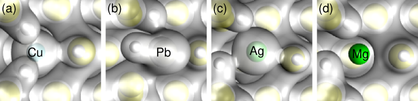
The electron densities for all four impurities adsorbed at site F on a dihydride step are shown in Figure 3. Cu, Ag and Mg all sit between the three surrounding Hs, close to the topmost Si layer. In the case of Ag and Mg [Figs. 3 (c) and (d)], the horizontal dihydrides (seen at the left side of the images) twist, while in the presence of Cu the structure of the step is almost undisturbed. Also, while Cu clearly forms bonds with the hydrogens, the electron cloud surrounding Ag only slightly overlaps with the electrons of the Hs. Mg loses its electrons completely and becomes ionic so no bonds are seen (the core electrons are not plotted). Pb is shown in the Si–Pb–H state, where it has replaced a H that was bonded with the Si in the lower left corner of the image.
3.2 Clustering of adsorbed impurities
Although the calculated adsorption energetics agree with experiments by suggesting that Cu and Pb can adsorb on the Si surface while other impurities cannot, they do not explain, for instance, how Cu changes the surface morphology of the (110) orientation to that covered in hillocks and Pb only slows down the etch rate [7]. In [24], it was argued based on KMC simulations that Cu impurities should be able to cluster on the surface and that these clusters are necessary to stabilize the apices of the hillocks. Therefore, studying the tendencies of Cu and Pb to form clusters on the surface may be the key to understanding the mechanisms by which the impurities influence the etching process. We calculate the structures and relative energies of Cu and Pb clusters of up to four impurity atoms on a (111) terrace. As the size of the cluster is increased, the number of possible stable or metastable structures also increases. Some of the energetically most favored configurations are shown in Figure 4.
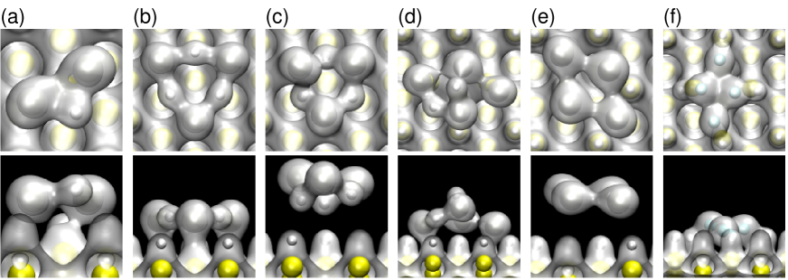
Like individual Pb atoms, Pb atoms in clusters can replace Hs on the surface [see Figs. 4 (a), (b), and (d)]. In this case the Pb atoms bond strongly with the exposed Si atoms and the removed H atoms become a part of the cluster. The other possibility is that the Pbs cluster with each other and this cluster then weakly adsorbs on the surface [Figure 4 (e)]. For a Pb dimer, the energy of a Pb-H-Pb structure shown in Figure 4 (a) is 0.99 eV below the energy of a weakly adsorbed Pb-Pb structure. (This latter structure truly is weakly adsorbed: it has an adsorption energy of only 0.14 eV.) For a Pb trimer, the most stable structure found is the symmetric Pb3H3 ring shown in Figure 4 (b). Each Pb in the ring has bonded with a Si by replacing a H and these Hs then connect the Pb atoms to each other.
We also calculate the binding energy of a Pb3H3 ring on an undisturbed H-terminated surface [Figure 4 (c)] and find that there is no interaction with the surface: the adsorption energy is only 0.06 eV. This means that if the Pb atoms reacted with the H2 released in etching by forming such clusters already in the etchant, these clusters would not adsorb at all. Therefore, the hydrogen in the adsorbed clusters should at least initially come from the Hs removed from the surface by the Pb replacement reaction.
For tetramers, the only stable symmetric structure found is a metallic Pb4 cluster [Figure 4 (e)] despite running several calculations starting from various initial configurations. Even if the initial configuration is symmetric, the structural optimization results in the tetramer breaking up. The tetramer structure with the lowest calculated energy is shown in Figure 4 (d). Two Hs have been removed from the surface and the left- and rightmost Pb atoms are bonded with Si. The Hs have moved to the left side of the cluster while the top- and rightmost Pbs in the image are only weakly interacting with the other Pb and H atoms. Interestingly, the energy of the weakly adsorbed Pb4 [Figure 4 (e)] is only 0.23 eV above the energy of this Pb4H2 tetramer, and all other calculated tetramers containing strong Si–Pb bonds have an even higher energy. This suggests that as the number of Pb atoms increases, the purely metallic clusters become more favorable than the structures containing hydrogen atoms. On the other hand, since these clusters adsorb so weakly on the H-terminated surface, they should not influence the etching process by acting as pinning agents if they do indeed form.
Cu atoms on the other hand are eager to form clusters by bonding both with each other and with the H atoms on the surface, as shown for a tetramer in Figure 4 (f). This suggests that Cu should have no difficulties in forming quite large clusters on the surface. As a measure of the clustering tendency, we plot the binding energies of impurities in clusters as a function of cluster size in Figure 5. The binding energy is calculated as , where is the energy of the energetically most favorable system containing the Si(111) slab and an -mer. In other words, measures the energy gain from joining an impurity to a cluster of atoms to form the -mer against the energy associated with the adsorption of the impurity alone as a monomer. If is positive, clustering is favored.

We see that the graphs for Cu and Pb are qualitatively different. is 0 eV by definition, and also the dimer binding energy is the same, 1.0 eV, for both metals. (Cf. with 0.9 eV for Cu in [24] calculated by comparing a system with a dimer to one with two monomers present.) Since the symmetric Pb3H3 ring is very stable, is 1.72 eV for Pb whereas it is only 0.79 eV for Cu, i.e., even slightly lower than . Most importantly though, for Pb drops dramatically to only 0.48 eV, more than one eV below the trimer binding energy. Cu behaves in a completely opposite way as climbs to 1.94 eV. Despite the small decrease at , the binding energies for Cu seem to grow when cluster size increases. (The average binding energy per Cu atom, , does always increase as a function of .) This indicates that it is energetically favorable to create quite large clusters. The binding energies of Pb in dimers and trimers are also considerable suggesting that also Pb may form clusters. However, the slump seen in tetramer binding energies means that although joining a Pb in a trimer in order to form a tetramer is energetically slightly better than having a monomer and a trimer [], it is more favorable to join the Pb with another monomer or a dimer []. The optimal Pb configuration may in fact consist of many small clusters — preferably the ring-shaped trimers — and of no large complexes. (The average binding energy per Pb atom is lower in tetramers than in trimers.)
3.3 Influence of impurities on etching
In order to quantify how clustering of impurities affects the etching process, we simulate the etching of (110) and (100) surfaces. Cu is simulated as an impurity that forms clusters. The site specific adsorption rates for Cu are set to be the same as in [24], following the first-principles adsorption activation energy hierarchy. Pb on the other hand is treated as an impurity that does not cluster. Although our first-principles results suggest that Pb may form clusters of a few atoms, the pinning effect of such small particles should not be much stronger than that of individual atoms and so we ignore the formation of Pb clusters altogether. We use a constant adsorption rate for Pb everywhere since the adsorption energy barriers should be low according to the first-principles results. Figure 6 shows the time evolution of the (110) surface in simulated etching at high etchant concentration and the (100) surface at low concentration (see Table LABEL:table:rates). We study these specific surfaces and conditions since trapezoidal and pyramidal hillocks are seen in the corresponding experiments [19].
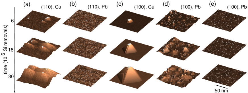
In Figure 6 (a), Cu clusters are seen on (110) and trapezoidal hillocks develop underneath. Since the lifetime of the clusters and also hillocks is long, the limited size of the simulated system is reached and the hillocks start merging. Conversely, there is no mechanism that drives cluster formation in the Pb simulations. Since Pb adsorption is uniform, the impurities are scattered randomly on the surface, as shown in Figure 6 (b). The surface morphology remains unchanged as etching proceeds.
In Figure 6 (c), the (100) surface is seen when etched under the influence of Cu. A Cu cluster is protecting the apex of a pyramidal hillock. Again, the hillock is stable enough to grow until it reaches the size of the simulation supercell. The effect of Pb on simulated (100) depends on the etchant concentration, however. If the etching of dihydride steps is fast enough with respect to the monohydrides (as in Table LABEL:table:rates), small hillocks are seen [Figure 6 (d)]. Since the ridges of the hillocks consist of Si atoms similar to those on monohydride steps and the facets are formed by (111) terraces, the hillocks become very stable in these conditions and even individual impurities can stabilize them. Still, the impurities are removed from the surface quite quickly due to underetching and the lifetime of these hillocks is short. The steady state morphology of the surface, where the surface is textured with the small hillocks and their remains, is reached quickly. If the relative stability of monohydrides is weakened slightly (the removal rates of Si atoms on monohydride step and kink sites are increased by a factor of 10 from the previous situation), hillocks remain quite stable and grow underneath impurity clusters [Figure 6 (c)] but not individual impurities [Figure 6 (e)] due to faster underetching.
Since the simulated Cu clusters are so stable that they enable hillocks to grow larger than feasible simulation cell sizes, it is not possible to reliably measure the impurity effect on etch rate and surface roughness from these simulations. In addition, the applied simulation method does not include the necessary effects to simulate e.g. the formation of deep etch pits which also affect these properties. Still, we make a qualitative comparison between the different cases presented above by calculating the etch rates and roughnesses (standard deviation of height). The properties are calculated for 120 nm120 nm systems with 435 impurity atoms present [3 impurities/(10 nm)2] after 30 million Si removal events (etch rate is measured for the final 6 million events) and averaged over five simulations. The obtained values are plotted in Figure 7. In addition to simulating etching with Cu and Pb, we also investigate the case where no impurities are adsorbing on the surface. Note that while the surfaces containing Pb or other non-adsorbing impurities reach a steady state during the simulation, the systems with Cu do not.
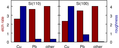
For (110), we find that Cu greatly increases surface roughness compared to when no impurities are present since it induces hillock growth. Cu also lowers the etch rate considerably. Pb on the other hand affects neither the surface morphology nor roughness. Pb does lower the etch rate, though. In fact, the simulated etch rate decreases further when the impurity concentration is increased (not shown). The relative etch rates of (100) with the different impurities are very close to those obtained for (110): Cu and Pb decrease the etch rate by about one third and one eighth, respectively. The Pb roughness shown as a blue bar in Figure 7 corresponds to the morphology of Figure 6 (d) with small hillocks. The roughness of this surface is twenty times the roughness of the systems with no adsorbing impurities, although still clearly below the roughness obtained with Cu. [The undisturbed simulated (100) is almost atomistically smooth.] For the hillockless morphology of Figure 6 (e) (white bar in Figure 7), roughness is almost as low as for the system with no impurities. Similar change in etching conditions has only a marginal effect for the other impurities and also the average etch rate with Pb remains virtually unchanged between the systems shown in Figs. 6 (d) and (e).
4 Discussion
Tanaka et al. [7] explained the experimentally observed effects of Cu and Pb on the etching process using an argument based on the oxidation-reduction potentials at high pH: Since the potentials of Cu and Pb, 0.40 and 0.91 V, respectively, are roughly the same or higher than that of hydrogen, 0.85 V, the H2 released in the etching process reduces the ionic impurities to a neutral state allowing them to adsorb in metallic form. Most of the impurities have low potentials and thus they remain as ions that do not adsorb. On the other hand, the potential of Ag is high, 0.40 V, and it should also be in the metallic state according to this argument. However, since our calculations show that the adsorption energy of metallic Ag on the H-terminated Si surface is close to zero, we argue that Ag does not adsorb even in the neutral state and thus it does not affect the etching reactions.
The tendency to react with the surface seen with Pb but not with the other impurities can be understood by examining electronegativities. Pb is more electronegative than H, the Pauling values being 2.3 and 2.2, respectively, and so Pb seeks additional electrons more eagerly than H. Therefore, instead of only bonding with the surface hydrogens, it is energetically favorable for Pb to bond directly with the silicons in a Si–Pb–H structure where a H is replaced by the Pb. Since Cu and Ag have lower electronegativities, 1.9 both (same as Si), they cannot replace Hs like Pb can. The electronegativity of Mg is so low (1.3) that the atom would give away its outer electrons to the Si surface if it was adsorbing in the neutral state, as seen in Figure 3 (d). (Although, according to the argument based on oxidation-reduction potentials, Mg should not be adsorbing in the neutral state in the first place.)
The adsorption behavior of Cu and Pb are qualitatively different. Cu adsorption energies are strongly site-specific while for Pb the adsorption energy depends mostly on the type of adsorption state rather than the adsorption site. However, the most important qualitative difference between Cu and Pb, when etching is considered, is the clustering tendency of Cu. Although the first-principles calculations do not prove that Pb cannot cluster on the Si surface, they suggest that Pb forms only small complexes. The energetically most favorable configuration found for Pb is a trimer. If the number of Pb atoms is increased, a metallic cluster consisting purely of Pb may become the lowest energy configuration. However, according to the first-principles calculations, such Pb clusters interact only weakly with the H-terminated surface (unlike Cu clusters). In this regard the two different adsorption states of Pb play an important part in separating Pb and Cu, since Pb needs to replace the hydrogens on the surface in order to adsorb strongly — something the metallic cluster does not do.
The surface morphology features obtained in KMC simulations based on the picture of impurities that either do or do not form clusters agree with experimentally seen morphologies and support the idea. More importantly, the estimated etch rate and surface roughness trends for (110) agree with the measured values in [6]. In experiments, Cu was seen to increase surface roughness by a factor of four by inducing the growth of hillocks. Cu also lowered the experimentally measured etch rate by some tens of percents depending on the Cu concentration. These effects are also seen in the simulations. (The increase in simulated roughness is by a factor of eight instead of four, though, and it would be even greater if the simulated systems were larger. However, the surfaces seen in experiments are much rougher than what can be realized in the small simulated systems in any case.) The increased roughness is obviously due to hillocks but, in fact, so is the decreased etch rate: The rapidly etching (110) floor gets replaced by the approximately {311} oriented, slowly etching hillock facets and this slows down the average etch rate of the whole surface [6, 19]. Pb on the other hand does not affect the surface roughness but lowers the etch rate, again in agreement with the experiments. This is due to the impurities adsorbing on the surface and slowing the etching process locally. Since the Pbs constantly desorb and adsorb, the morphology is left unchanged and effectively the etch rate of the whole surface is decreased. Increasing the number of Pb atoms in the simulation decreases the average etch rate even further. This is true also in the experiments up to a concentration of 100 ppb [6].
We are not aware of experiments where (100) is etched at low etchant concentration while Cu and Pb concentrations are manipulated. [Such experiments exist for (100) at high concentration, though, but in such conditions the presence of Cu impurities leads to the appearance of round pits instead of hillocks [7].] Still, it is experimentally known that pyramidal hillocks are common in these etching conditions [19, 5, 12, 13], although, their appearance may often be induced by other means than a high concentration of metal impurities, e.g., by hydrogen bubbles [5, 8, 9]. The KMC simulations, where these additional factors are not present, predict that large pyramidal hillocks can be stabilized by Cu clusters just like the trapezoidal hillocks on (110). In addition, the presence of Pb impurities may also be sufficient for inducing the growth of small hillocks. The stability of these small hillocks depends quite delicately on the etching conditions, though, and it is possible that they do not appear in real etching.
5 Conclusions
We have demonstrated using first-principles calculations that Cu and Pb adsorb on the hydrogen-terminated Si surface while other common metal impurities, represented by Mg and Ag, do not. This explains why only Cu and Pb have been observed to affect the wet etching process of Si. The adsorption energies of Cu depend strongly on the adsorption site whereas Pb adsorption is quite homogeneous. Furthermore, calculated energies of clusters of up to four metal atoms on the surface indicate that it is energetically favorable for Cu to form large clusters, while for Pb the optimal size of a strongly adsorbed cluster is three Pb atoms. Clusters of four Pb atoms containing H tend to break suggesting that large Pb clusters adopt a metallic state. However, these metallic clusters interact very weakly with the H-terminated Si surface and so only the small Pb clusters may act as micromasks during etching. This picture is supported by kinetic Monte Carlo simulations of wet etching of Si in which clusters of adsorbed impurities lead to rough surfaces and decreased etch rates (compared to etching in the absence of impurities) while individually adsorbed impurities lower the etch rate but do not affect the surface roughness. These two types of behavior correspond to, and explain, the experimentally observed effects of Cu and Pb impurities, respectively.
References
- [1] D. Saya, K. Fukushima, H. Toshiyoshi, G. Hashiguchi, H. Fujita, and H. Kawakatsu. Sensors and Actuators A, 95:281, 2002.
- [2] J. W. Kwon and E. S. Kim. Sensors and Actuators A, 97-98:729, 2002.
- [3] Gerold Schröpfer, Michel de Labachelerie, Sylvain Ballandras, and Pascal Blind. J. Micromech. Microeng., 8:77, 1998.
- [4] M. A. Hines. Annu. Rev. Phys. Chem., 54:29, 2003.
- [5] S. A. Campbell, K. Cooper, L. Dixon, R. Earwaker, S. N. Port, and D. J. Schiffrin. J. Micromech. Microeng., 5:209, 1995.
- [6] H. Tanaka, Y. Abe, T. Yoneyama, J. Ishikawa, O. Takenaka, and K. Inoue. Sensors and Actuators A, 82:270, 2000.
- [7] H. Tanaka, D. Cheng, M. Shikida, and K. Sato. Sensors and Actuators A, 128:125, 2006.
- [8] H. Schröder, E. Obermeier, and A. Steckenborn. J. Micromech. Microeng., 9:139, 1999.
- [9] W. Haiss, P. Raisch, L. Bitsch, R. J. Nichols, X. Xia, J. J. Kelly, and D. J. Schiffrin. J. Electroanal. Chem., 597:1, 2006.
- [10] S. P. Garcia, H. Bao, and M. A: Hines. Phys. Rev. Lett., 93:166102, 2004.
- [11] M. A. Gosálvez, Y. Xing, T. Hynninen, M. Uwaha, A. S. Foster, R. M. Nieminen, and K. Sato. J. Micromech. Microeng., 17:S27, 2007.
- [12] A. J. Nijdam, E. van Veenendaal, H. M. Cuppen, J. van Suchtelen, M. L. Reed, J. G. E. Gardeniers, W. J. P. van Enckevort, E. Vlieg, and M. Elwenspoek. J. Appl. Phys., 89:4113, 2001.
- [13] E. van Veenendaal, K. Sato, M. Shikida, A. J. Nijdam, and J. van Suchtelen. Sensors and Actuators A, 93:232, 2001.
- [14] M. A. Gosálvez and R. M. Nieminen. New J. of Phys., 5:100, 2003.
- [15] M. Shikida, T. Masuda, D. Uchikawa, and K. Sato. Sensors and Actuators A, 90:223, 2001.
- [16] E. van Veenendaal, K. Sato, M. Shikida, and J. van Suchetelen. Sensors and Actuators A, 93:219, 2001.
- [17] S. P. Garcia, H. Bao, and M. A. Hines. J. Phys. Chem. B, 108:6062, 2004.
- [18] H. Tanaka, S. Yamashita, Y. Abe, M. Shikida, and K. Sato. Sensors and Actuators A, 114:516, 2004.
- [19] M. A. Gosálvez, K. Sato, A. S. Foster, R. M. Nieminen, and H. Tanaka. J. Micromech. Microeng., 17:S1, 2007.
- [20] H. Tanaka, D. Cheng, M. Shikida, and K. Sato. Sensors and Actuators A, 134:465, 2007.
- [21] J. Rappich, H. J. Lewerenz, and H. Gerischer. J. Electrochem. Soc., 140:L187, 1993.
- [22] P. Allongue. Phys. Rev. Lett., 77:1986, 1996.
- [23] A. S. Foster, M. A. Gosálvez, T. Hynninen, R. M. Nieminen, and K. Sato. Phys. Rev. B, 76:075315, 2007.
- [24] T. Hynninen, M. A. Gosálvez, A. S. Foster, H. Tanaka, K. Sato, M. Uwaha, and R. M. Nieminen. New J. of Phys., 10:013033, 2008.
- [25] J. Junquera, Ó. Paz, D. Sánchez-Portal, and E. Artacho. Phys. Rev. B, 64:235111, 2001.
- [26] J. M. Soler, E. Artacho, J. D. Gale, A. García, J. Junquera, P. Ordejón, and D. Sánchez-Portal. J. Phys.: Condensed Matt., 14:2745, 2002.
- [27] P. Hohenberg and W. Kohn. Phys. Rev., 136:B864, 1964.
- [28] W. Kohn and L. J. Sham. Phys. Rev., 140:A1133, 1965.
- [29] J. P. Perdew, K. Burke, and M. Ernzerhof. Phys. Rev. Lett., 77:3865, 1996.
- [30] S. F. Boys and F. Bernadi. Mol. Phys., 19:553, 1970.
- [31] M. A. Gosálvez, A. S. Foster, and Risto M. Nieminen. Appl. Surf. Sci., 202:160, 2002.
- [32] J. L. Blue, I Beichl, and F. Sullivan. Phys. Rev. E, 51:R867, 1995.
- [33] M. A. Gosálvez, Y. Xing, K. Sato, and R. M. Nieminen. J. Micromech. Microeng., 18:055029, 2008.
- [34] Z. Zhou, Q. Huang, W. Li, and W. Deng. J. Micromech. Microeng., 17:S38, 2007.
- [35] M. A. Gosálvez, Y. Xing, and K. Sato. J. Microelectromech. Syst., 17:410, 2008.
- [36] B. Delaunay. Otdelenie Matematicheskikh i Estestvennykh Nauk, 7:793, 1934.