Proposal for a nanoscale variable resistor/electromechanical transistor
Abstract
A nanoscale variable resistor consisting of a metal nanowire (active element), a dielectric, and a gate, is proposed. By means of the gate voltage, stochastic transitions between different conducting states of the nanowire can be induced, with a switching time as fast as picoseconds. With an appropriate choice of dielectric, the transconductance of the device, which may also be considered an “electromechanical transistor,” is shown to significantly exceed the conductance quantum , a remarkable figure of merit for a nanoscale device.
Index Terms:
Nanotechnology, Varistors, Transistors, Electromechanical effects.I Background
Metal nanowires have attracted considerable interest in the past decade due to their remarkable transport and structural properties [1]. Long gold and silver nanowires were observed to form spontaneously under electron irradiation [2, 3, 4], and appear to be surprisingly stable. Even the thinnest gold wires, essentially chains of atoms, have lifetimes of the order of seconds at room temperature [5]. Metal nanowires exhibit striking correlations between their stability and electrical conductance [6, 7]. That these filamentary structures are stable at all is rather counterintuitive [8, 9], but can be explained by electron-shell effects [10, 11, 8, 9, 12].
Because most of their atoms are at the surface, with low coordination numbers, metal nanowires behave essentially like fluids [9]. Classically, the Rayleigh instability would break up any wire whose length exceeds its circumference [8]. Nevertheless, nanowires violating the Rayleigh criterion have been observed [2, 3, 4]. The instability is suppressed through quantum effects, with stabilization occurring through the nanowire’s electronic shell structure. A quantum linear stability analysis [8, 13, 14, 15] showed the existence of “islands of stability” for discrete intervals of the radius . These correspond to conductance “magic numbers” that agree with those observed in experiments. For low enough temperatures, there remain finite regions of stable against long-wavelength perturbations. Therefore, stable wires exist only in the vicinity of certain “magic radii” and consequently at quantized conductance values that are integer multiples of the conductance quantum .
However, the linear stability analysis ignores large thermal fluctuations that can lead to breakup of the wire. Nanowire lifetimes are inferred from conductance histograms, compiled by cycling a mechanically controllable break junction (MCBJ) thousands of times [10, 16, 11]. These studies indicate that conductance peaks disappear above fairly well-defined temperatures.
Bürki et al. [17] studied the lifetimes of these nanowires using techniques developed in [18]. By modelling thermal fluctuations through stochastic Ginzburg-Landau classical field theories, they constructed a self-consistent approach to the fluctuation-induced “necking” of nanowires that is in good agreement with experiment [17, 19]. Their theory indicates that passivated noble metal nanowires are sufficiently stable at room temperature to serve as interconnects between nanoscale circuit elements.
Of particular interest for the applications considered in this proposal is the nature of the barriers separating wires of different magic radii (and hence quantized conductances). These barriers can be surmounted in several ways: among them are raising the temperature, applying strain, shortening the wire, or changing the Fermi energy. The first three are discussed in [17, 19], but the last is new to this proposal. For the purposes of a new nanoscale device, the first two may be unsatisfactory for various reasons having to do either with nonoptimal operating conditions (temperature), or probable inability to implement these controls on the nanoscale (strain).
On the experimental side, nanowires suitable for the proposed device, i.e. with conductance between a few and a few hundred conductance quanta, and lengths below or around a few nanometers have been fabricated using various techniques, including scanning tunnelling microscopy (STM) [20, 21], MCBJ [22, 10], thin-film transmission electron microscopy (TEM) [2, 23], electromigration [24], and electrochemical fabrication [25]. Nanowires with diameters less than a nanometer have been directly observed [2] using TEM to remain stable under low beam intensities below for the duration of observation. Stochastic switching between different conductance values has been observed in contacts made using MCBJ [26], while controllable switching has been achieved recently using electromigration to grow or shrink a nanobridge between two wires [27]. A structural thinning process of the nanowire similar to the one described by the theory of Bürki et al. [17, 28] has been observed to take place for gold nanowires in TEM experiments. The nanowire was observed [4] to thin step by step via a process where a structural step (corresponding to a change in radius of the order one atomic diameter) forms at one end of the wire and subsequently propagates along the wire.
II Description of the device
Variable resistors are commonly used circuit elements in many electronic applications. However, their large size and slow response time have heretofore limited their use primarily to the human-circuit interface. In this article, we describe how the exploitation of quantum and stochastic effects at the nanoscale allows one to combine what would ordinarily be distinct macroscale circuit elements into a single nanoscale device with multiple functionalities, and to achieve response times on the order of picoseconds.

.
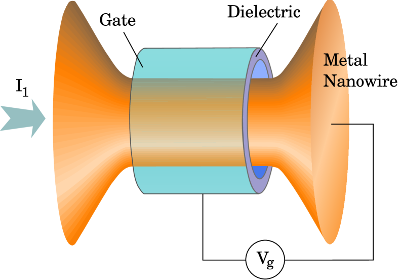
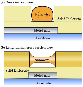
The proposed device is illustrated in Fig. 1. The physics behind its operation is the following: A metal nanowire is the active circuit element, and is embedded in a dielectric sheath, surrounded by an outer conductor of comparable dimensions, referred to as the gate. A positive/negative voltage applied to the gate enhances/depletes the density of carriers in the nanowire. Importantly, the resulting shift in the Fermi energy alters the electron-shell structure of the nanowire, which in turn determines its stability.
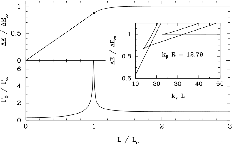
The magic radii are the minima of the electron-shell potential (see Fig. 2, and e.g. [12]), which depends on the dimensionless parameter , with the Fermi wavevector and the wire radius. A shift in is thus analogous to applying strain, and can be used to induce rapid (i.e., on the scale of the Debye frequency) transitions between neighboring magic radii. These have conductances differing by , where is an integer (see Fig. 2). (As a rule of thumb, the jumps scale as for a wire with initial radius .) The switching time between two adjacent magic radii was shown [17] to be given by the Kramers formula
| (1) |
where is the energy barrier, is Boltzmann’s constant, and is the temperature. The rate prefactor , of order the Debye frequency, was calculated explicitly in Ref. [17]. The dependence of on the parameter is illustrated in Fig. 3.

The possibility of shifting electrostatically, as described above, depends in an essential way on the crucial feature that the nanowire has a radius of order nanometers, and thus has a very low density of states at . As a function of the applied gate voltage , the shift in is given by [29]
| (2) |
where is the mutual capacitance between gate and nanowire, and is the density of states of the nanowire at . As discussed in [29], the denominator in Eq. (2) can be well approximated in terms of material and geometrical parameters, yielding a convenient rule-of-thumb estimate
| (3) |
where is the Fermi gas parameter for the nanowire material (essentially the mean interelectron separation in the bulk metal), is the mean dielectric constant of the dielectric sheath, and is a dimensionless parameter of order unity, which depends logarithmically on the device dimensions (Fig. 1).
In order to achieve the maximum switching speed, it is necessary to achieve a shift in the shell-potential parameter. From Eq. (3), this implies a preferred operating gate voltage
| (4) |
For typical metals, –3, while in the domain of validity of the nanoscale free electron model [30, 31]. It is therefore desirable to use a dielectric with to minimize the necessary gate voltages.
II-A Transconductance
Because the mechanical switching time of the nanoscale variable resistor can be as short as picoseconds, it may also be thought of as an electromechanical transistor. It is thus useful to compute its transconductance, a figure of merit used to characterize transistors. The transconductance can be estimated as
| (5) |
Using Eq. (4) and , one finds
| (6) |
For large dielectric constants , and bias voltages V, one can thus achieve , an exceptional figure of merit for a nanoscale device [32], thereby enabling its advantageous use as an effective transistor. In addition to the structural switching time of order picoseconds, the electrical rise time can be estimated to be of order 1 femtosecond for typical device dimensions/materials, and so is not a limiting factor in device performance.
II-B Ohmicnon-Ohmic transition
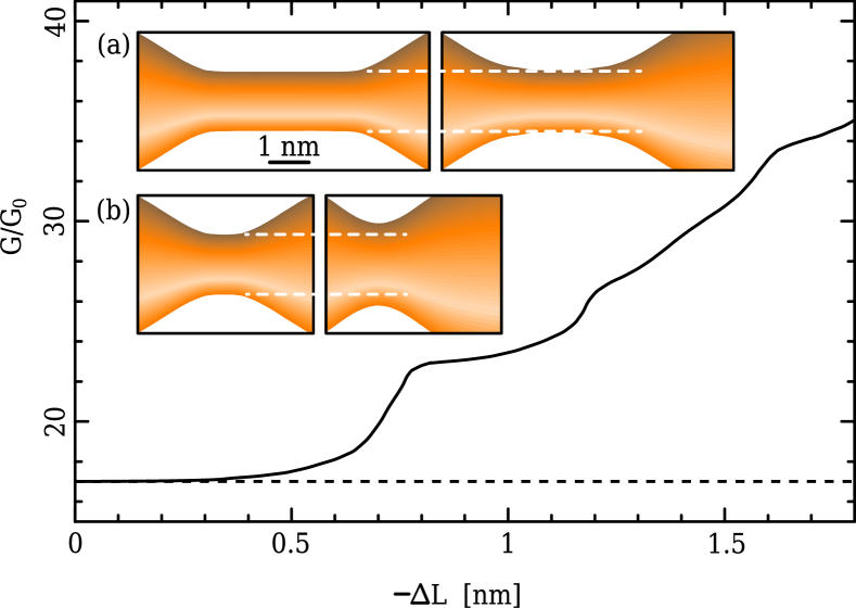
The device discussed above is one where barriers are controlled by shifting the Fermi energy of the nanowire through electrostatic means. Another possibility is to change the wire length. In [17] it was predicted that a transition in activation behavior occurs as a function of wire length: below a critical length , the barrier decreases rapidly with length, while above it is roughly constant. The transition can be continuous (second-order) or discontinuous (first-order) (see Fig. 4). This effect may have already been observed: a recent study [33] reported a transition from linear to nonlinear behavior in gold nanowires, as distance between electrodes shortened due to applied bias. In a Comment [19], we were able to explain this result as a consequence of the transition in radius stability as a function of wire length (cf. Fig. 4). This leads to another device possibility, namely changing wire length directly by changing the applied voltage. This would convert a wire with linear characteristics to one with nonlinear ones (see Fig. 5). At the present time, it remains unclear how easily controllable such a transition might be.
III Fabrication of the device
Commercial fabrication of a nanoscale variable resistor/electromechanical transistor will require combining the three components of the device—metal nanowire, dielectric, and gate—integrated with other circuitry on a chip. Accordingly, the formation of the nanoscale circuitry may be based on the following steps:
Step 1: The initial structure of the nanowire, including its electrical connection to the rest of the integrated circuit, can be formed with standard semiconductor fabrication and patterning processes such as for example E-beam direct write, or alternatively in the long term masked ion beam lithography, to deposit a metal wire tens of nanometers in diameter on the substrate (e.g., a Si wafer or other insulating substrate). Suitable metals for nanowire formation include Au, Ag, Cu, Pt, and Al, among others.
Step 2: To form an active device, a short section of the nanowire must be thinned down to a diameter of order one nanometer using e.g. a focused scanning electron microscope (SEM), electromigration [34, 35, 36], chemical etching [25], or a combination of these techniques.
Step 3: The active segment of the nanowire must be encased in dielectric, which also serves to passivate the nanowire surface, increasing durability.
Step 4: The nanowire encased in dielectric must be placed in proximity to one or more metal gates, used to control the nanowire resistance through induced structural transitions.
III-A Dielectric
To achieve optimal device characteristics, the space between the active segment of the nanowire and the gate(s) should be filled with a dielectric with . If a solid dielectric (only) is used, a small gap around the active segment of the nanowire must be provided (see Figure 7(b)) to permit the nanowire surface to fluctuate freely. In that case, the mean dielectric constant of the region between the nanowire and the gate(s) (including the gap) should exceed ten. Many intrinsic semiconductors could serve as suitable solid dielectrics with (e.g., Si, Ge, InSb, InAs, InP, GaSb, or GaAs). The material should be chosen so that the semiconducting energy gap exceeds the maximum desired voltage difference between the gate and nanowire.
A liquid dielectric or combination of solid and liquid dielectrics could also be utilized. This would allow for optimal filling of the dielectric region, while still permitting free motion of the nanowire surface. Liquid dielectrics have been used in conjunction with some of the previous techniques [37, 38, 25], in the context of single molecule measurements, as well as for STM measurements of metal contact transport. In the latter context, they have been shown to have little influence on the stability and transport properties of the nanocontact [38].
Liquid dielectrics can have large dielectric constants and, being liquids, would easily adapt to the shape of the nanowire, without preventing its deformation. They are thus ideal candidates for the proposed device. For example, the dielectric constant of water at room temperature is close to 80. While the finite conductivity of water might be problematic, deionized water still has a dielectric constant of 15. As another example, Glycerol has a dielectric constant above 40. Various oil-based dielectrics [see e.g. US patent No 413189] have been developed and could be suitable for the proposed device. Alternatively, a dielectric gel or sol-gel or a combination of solid and gel dielectrics can be placed between the active segment of the nanowire and the gate(s).
IV Examples
Examples of specific nanowire devices are provided below. It is important to note that the device architectures described in the examples are generic in nature, and the list of examples included is not intended to be exhaustive.
Example 1
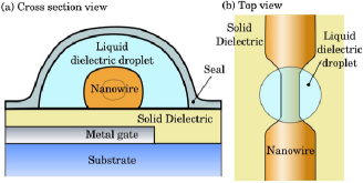
In one embodiment of the proposed device (see Figure 6), a layer of solid dielectric is deposited on a substrate prepatterned (using standard vapor deposition techniques) with a metallic gate to address the nanowire device. A metal nanowire several tens of nanometers in diameter with a “notch” or constriction at the desired location is then deposited on the surface of the dielectric, in alignment with the submerged gate electrode. The nanowire at the notch can then be thinned down to the specified operating diameter by electromigration, SEM, or chemical etching. A nanodroplet of liquid dielectric is then deposited on the surface of the wafer, immersing the nanowire device (see Figure 6). The nanowire device, together with the droplet of liquid dielectric, is then hermetically sealed, e.g., with an epoxy seal.
Example 2
In another embodiment of the proposed device (see Figure 7), a layer of solid dielectric is deposited on a substrate prepatterned with a metallic gate to address the nanowire device, as in Example 1. A metal nanowire of uniform diameter several tens of nanometers is then deposited on the surface of the dielectric, in alignment with the submerged gate electrode. This fabrication step can be carried out within standard semiconductor patterning techniques, such as for example E-beam direct write or alternatively in the long term masked ion beam lithography. A further layer of solid dielectric is then deposited, fully encasing the nanowire. A nanoscale pit or cavity is then etched in the dielectric layer, exposing the active segment of the nanowire. The exposed segment of the nanowire is then thinned down to the specified diameter (of order one nanometer) via e.g., focused SEM, chemical etching, or electromigration, or a combination of these techniques.
A hermetic seal can be applied to increase the durability of the nanowire device. For example, an epoxy bubble seal may be used to enclose an inert atmosphere (e.g., nitrogen or argon) about the exposed segment of the nanowire. Alternatively, a passivation layer over the nanowire device is used to scavenge any small amounts of oxidant from the sealed environment.
The pit containing the nanowire (see Figure 7(b)) can also be filled with a liquid or gel dielectric before the seal is applied, to enhance device performance.
For some applications, both a top gate (not shown) and a bottom gate are included, above and below the nanowire device, respectively. Multiple gates may be desirable e.g. to address individual devices in a large array. For example, if the gate voltage is chosen appropriately, the device will switch conducting states rapidly only if the voltage is applied to both gates.
Example 3
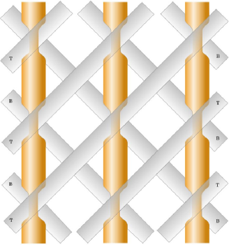
In order to individually address individual devices in a large array on a chip, it may be desirable to fabricate a criss-crossing pattern of top and bottom gates (see Figure 8). With an appropriate choice of operating voltages, only the nanowire device located at the intersection of the two active gates is addressed, and caused to switch conducting states.
Because the three (or more) terminals of the nanoscale variable resistor are comprised of metal patterned by standard semiconductor fabrication techniques, such devices can be readily integrated with conventional circuitry on a chip. Because the throughput impedance of such a device is on the scale of several hundred to several thousand Ohms, appropriate amplification may be required to interface with standard CMOS circuitry.
Acknowledgments
This work was supported by NSF Grant Nos. 0312028 (CAS) and PHY-0651077 (DLS). Part of this work was done when CAS and DLS were at the Aspen Center for Physics.
References
- [1] N. Agraït, A. Levy Yeyati, and J. M. van Ruitenbeek, “Quantum properties of atomic-sized conductors,” Phys. Rep., vol. 377, pp. 81–279, 2003.
- [2] Y. Kondo and K. Takayanagi, “Gold nanobridge stabilized by surface structure,” Phys. Rev. Lett., vol. 79, no. 18, pp. 3455–3458, 1997.
- [3] V. Rodrigues, J. Bettini, A. R. Rocha, L. G. C. Rega, and D. Ugarte, “Quantum conductance in silver nanowires: Correlation between atomic structure and transport properties,” Phys. Rev. B, vol. 65, no. 15, p. 153402, 2002.
- [4] Y. Oshima, Y. Kondo, and K. Takayanagi, “High-resolution ultrahigh-vacuum electron microscopy of helical gold nanowires: junction and thinning process,” J. Electron Microsc., vol. 52, pp. 49–55, 2003.
- [5] R. H. M. Smit, C. Untiedt, and J. M. van Ruitenbeek, “High-bias stability of monatomic chains,” Nanotech., vol. 15, p. S472, 2004.
- [6] D. F. Urban, J. Bürki, A. I. Yanson, I. K. Yanson, C. A. Stafford, J. M. van Ruitenbeek, and H. Grabert, “Electronic shell effects and the stability of alkali nanowires,” Solid St. Comm., vol. 131, no. 9-10, pp. 609–614, 2004.
- [7] A. I. Mares, D. F. Urban, J. Bürki, H. Grabert, C. A. Stafford, and J. M. van Ruitenbeek, “Electronic and atomic shell structure in aluminum nanowires,” Nanotechnology, vol. 75, no. 26, p. 265403, 2007.
- [8] F. Kassubek, C. A. Stafford, H. Grabert, and R. E. Goldstein, “Quantum suppression of the rayleigh instability in nanowires,” Nonlinearity, vol. 14, pp. 167–177, 2001.
- [9] C.-H. Zhang, F. Kassubek, and C. A. Stafford, “Surface fluctuations and the stability of metal nanowires,” Phys. Rev. B, vol. 68, p. 165414, 2003.
- [10] A. I. Yanson, I. K. Yanson, and J. M. van Ruitenbeek, “Observation of shell structure in sodium nanowires,” Nature, vol. 400, pp. 144–146, 1999.
- [11] A. I. Yanson, J. M. van Ruitenbeek, and I. K. Yanson, “Shell effects in alkali metal nanowires,” Low Temp. Phys., vol. 27, pp. 807–820, 2001.
- [12] J. Bürki, R. E. Goldstein, and C. A. Stafford, “Quantum necking in stressed metallic nanowires,” Phys. Rev. Lett., vol. 91, p. 254501, 2003.
- [13] D. F. Urban and H. Grabert, “Interplay of Rayleigh and Peierls instabilities in metallic nanowires,” Phys. Rev. Lett., vol. 91, p. 256803, 2003.
- [14] D. F. Urban, J. Bürki, C.-H. Zhang, C. A. Stafford, and H. Grabert, “Jahn-teller distortions and the supershell effect in metal nanowires,” Phys. Rev. Lett., vol. 93, p. 186403, 2004.
- [15] D. F. Urban, J. Bürki, C. A. Stafford, and H. Grabert, “Stability and symmetry breaking in metal nanowires,” Physical Review B, vol. 74, p. 245414, 2006.
- [16] A. I. Yanson, I. K. Yanson, and J. M. van Ruitenbeek, “Supershell structure in alkali metal nanowires,” Phys. Rev. Lett., vol. 84, pp. 5832–5835, 2000.
- [17] J. Bürki, C. A. Stafford, and D. L. Stein, “Theory of metastability in simple metal nanowires,” Phys. Rev. Lett., vol. 95, p. 090601, 2005.
- [18] R. S. Maier and D. L. Stein, “Droplet nucleation and domain wall motion in a bounded interval,” Phys. Rev. Lett., vol. 87, p. 270601, 2001.
- [19] J. Bürki, C. A. Stafford, and D. L. Stein, “Comment on ‘Nonlinear current-voltage curves of gold quantum point contacts’,” Appl. Phys. Lett., vol. 88, p. 166101, 2006.
- [20] N. Agraït, J. G. Rodrigo, and S. Vieira, “Conductance steps and quantization in atomic-size contacts,” Phys. Rev. B, vol. 47, pp. 12 345–12 348, 1993.
- [21] G. Rubio, N. Agraït, and S. Vieira, “Atomic-sized metallic contacts: mechanical properties and electronic transport,” Phys. Rev. Lett., vol. 76, pp. 2302–2305, 1996.
- [22] A. I. Yanson, G. Rubio Bollinger, H. E. van den Brom, N. Agraït, and J. M. van Ruitenbeek, “Formation and manipulation of a metallic wire of single gold atoms,” Nature, vol. 395, pp. 783–785, 1998.
- [23] Y. Kondo and K. Takayanagi, “Synthesis and characterization of helical multi-shell gold nanowires,” Science, vol. 289, pp. 606–608, 2000.
- [24] D. R. Strachan, D. E. Smith, D. E. Johnston, T.-H. Park, M. J. Therien, D. A. Bonnell, and A. T. Johnson, “Controlled fabrication of nanogaps in ambient environment for molecular electronics,” App. Phys. Lett., vol. 86, p. 043109, 2005.
- [25] H. X. He, S. Boussaad, B. q. Xu, C. Z. Li, and N. J. Tao, “Electromechanical fabrication of atomically thin metallic wires and electrodes separated with molecular-scale gaps,” J. Electroanal. Chem., vol. 522, pp. 167–172, 2002.
- [26] J. M. Krans, J. M. van Ruitenbeek, and L. J. de Jongh, “Atomic structure and quantized conductance in metal point contacts,” Physica B, vol. 218, pp. 228–233, 1996.
- [27] K. Terabe, T. Hasegawa, T. Nakayama, and M. Aono, “Quantized conductance atomic switch,” Nature, vol. 433, pp. 47–50, 2005.
- [28] J. Bürki, “Discrete thinning dynamics in a continuum model of metallic nanowires,” Physical Review B, vol. 75, p. 205435, 2007.
- [29] F. Kassubek, C. A. Stafford, and H. Grabert, “Force, charge, and conductance of an ideal metallic nanowire,” Phys. Rev. B, vol. 59, no. 11, pp. 7560–7574, 1999.
- [30] C. A. Stafford, D. Baeriswyl, and J. Bürki, “Jellium model of metallic nanocohesion,” Phys. Rev. Lett., vol. 79, pp. 2863–2866, 1997.
- [31] J. Bürki and C. A. Stafford, “On the stability and structural dynamics of metal nanowires,” Applied Physics A, vol. 81, no. 8, pp. 1519–1525, 2005.
- [32] D. M. Cardamone, C. A. Stafford, and S. Mazumdar, “Controlling quantum transport through a single molecule,” Nano Letters, vol. 6, p. 2422, 2006.
- [33] M. Yoshida, Y. Oshima, and K. Takayanagi, “Nonlinear current-voltage curves of gold quantum point contacts,” Appl. Phys. Lett., vol. 87, p. 103104, 2005.
- [34] W. J. Kim and M. N. Carr, S. M. Wybourneb, “Direct contact buckling of electrochemically grown gold nanowires,” Appl. Phys. Lett., vol. 87, p. 173112, 2005.
- [35] M. Saka and R. Ueda, “Formation of metallic nanowires by utilizing electromigration,” J. Mater. Res., vol. 20, no. 10, p. 2712, 2005.
- [36] G. Riveros, S. Green, A. Cortes, H. Gómez, R. E. Marotti, and E. A. Dalchiele, “Silver nanowire arrays electrochemically grown into nanoporous anodic alumina templates,” Nanotechnology, vol. 17, p. 561, 2006.
- [37] B. Xu, H. Huixin, and N. J. Tao, “Controlling the conductance of atomically thin metal wires with electrochemical potential,” J. Am. Chem. Soc., vol. 124, pp. 13 568–13 575, 2002.
- [38] H. X. He, C. Shu, C. Z. Li, and N. J. Tao, “Adsorbate effect on the mechanical stability of atomically thin metallic wires,” J. Electroanal. Chem., vol. 522, pp. 26–32, 2002.
| Jérôme Bürki received the Ph.D. degree in physics from the University of Fribourg, Switzerland, in 2000. From 2004 to 2008, he held a position of Research Associate in the Physics Department at the University of Arizona. He is currently Assistant Professor of Physics in the Department of Physics and Astronomy at California State University, Sacramento. His research focuses on quantum effects on various properties, including nonlinear dynamics, of metal nanostructures. |
| Charles A. Stafford received the Ph.D. degree in physics from Princeton University, Princeton, New Jersey, in 1992. Since 1998, he has been on the faculty of the Physics Department at the University of Arizona, where he is currently Associate Professor of Physics. His research has focused on strongly-correlated electron systems and, more recently, on quantum transport and cohesion in nanostructures. His current interests include electron transport in single-molecule heterojunctions and the structural dynamics of metal nanowires. |
| Daniel L. Stein received the Ph.D. degree in physics from Princeton University, Princeton, New Jersey, in 1979. Since 2005, he has been a Professor of Physics and Mathematics at New York University. His research in recent years has focused primarily on quenched disorder in statistical mechanical systems, particularly spin glasses, and on stochastic processes in both macroscopic and nanoscale systems. |