–Draft–
Surface waves in photonic crystal slabs
Abstract
Photonic crystals with a finite size can support surface modes when appropriately terminated. We calculate the dispersion curves of surface modes for different terminations using the plane wave expansion method. These non-radiative surface modes can be excited with the help of attenuated total reflection technique. We did experiments and simulations to trace the surface band curve, both in good agreement with the numerical calculations.
The most well-known feature of Photonic crystals (PCs) is the photonic band gap (PBG), inside which the electromagnetic waves are prohibited to propagate in all directions book Soukoulis . However, when appropriately terminated, PCs can support surface modes with frequencies lying inside the PBG book PC . Surface modes are easily obtained for one-dimensional PCs (stacks of alternating continuous layers) and their dispersion relation has been obtained experimentally and theoreticallysw3 .
For a 2D PC the existence of surface waves has been shown theoretically (in band structure calculations for semi-infinite PC) sw1 ; sw2 and experimentally by attenuated total reflection (ATR) measurements mit atr . Further numerical work has shown that the existence and dispersion of surface waves at a 2D PC are very sensitive to the surface termination sw2 ; observe surface state . When terminated improperly, both the poor impedance matching and the interaction with surface modes can disrupt the electromagnetic wave propagation and are bad to the performance of photonic devices such as PC waveguides and PC cavities observe surface state . Recent studies also show that when the PC is appropriately periodically corrugated at the surface, enhanced transmission and beaming of light can be achieved through a PC waveguide with a subwavelength width beaming 1 ; beaming 2 ; ozbay . This effect is due to the excitation of surface modes and constructive interference at the axis of the waveguide.
In this paper, we study experimentally and numerically the dispersion relation of surface modes for different surface corrugations that support surface waves. In contrast to previous work, we determine experimentally the complete dispersion relation of the surface modes within the photonic band gap of the PC.
In addition to the well-known theoretical band-structure calculations for the infinite periodic PC we also perform full-wave frequency-domain finite element (FEMLAB) simulations to determine the surface mode dispersion relation numerically for a finite PC and compare the three different approaches.
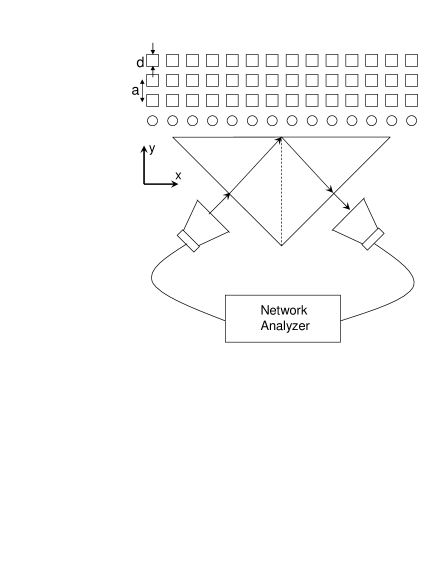
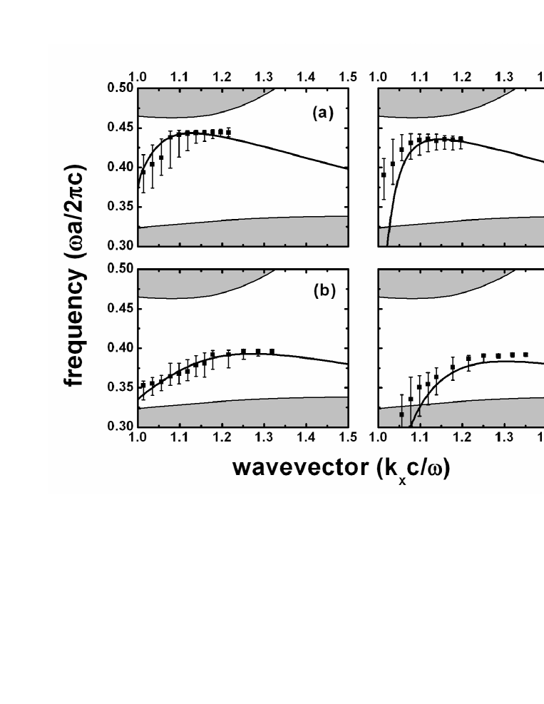
The 2D PC we study is a square array of square alumina rods, 21 layers in direction and 15 layers in direction. The lattice constant is and the square rods are of dimension with permittivity and height (Fig. 1). With the help of the supercell technique, the band structure of the finite-size PC can be calculated using the plane wave expansion method 1990 Ho . We studied TM (electric field along the rods) modes through out the work since only TM modes can give a full band gap for a two dimensional PC book PC . As shown, for example, in Fig.2 (a), the PC has a band gap in between the light gray areas. There are no modes inside the band gap.
The uncorrugated PC does not support surface waves (in the lowest total band gap); to observe surface modes we have to corrugate the surface layer of the PC, rendering it different from the air on one side and the PC bulk on the other side.
The actual shape of the corrugation layer elements is not very important. We use cylindrical rods of different diameters, but also cut semi-cylinders mit atr , rectangular cross-section rods different from the ones comprising the bulk PC square corrugation or geometrically identical rods with different dielectric constant might be used. However, there is no guarantee to obtain surface modes for a particular surface termination; the surface layer parameters have to be chosen carefully for the corrugated PC to support surface modes in the band gap of the bulk PC.
In order to support surface modes, we add a new layer at the surface of the PC with circular alumina rods as a periodic corrugation (Fig. 1). The band structure of the corrugated PC was calculated using the plane wave expansion and the supercell technique. The solid lines in Figures 2(a) and 2(b) show the dispersion relation of the surface modes which lie inside the band gap when the diameter of the circular rods is and , respectively. A surface mode cannot extend into the PC since the frequency is within the band gap. Nor can it extend into air because the surface mode lies to the right of the light line (). So this mode is localized to the surface of the structure and can be called a surface mode. The diameter of the corrugation rods needs to be chosen properly so that the surface dispersion lies within the band gap. When the surface mode goes out of the band gap, the mode can extend into the PC and is no longer a surface mode. Actually, a single layer of only dielectric rods surrounded by air can support surface modes. The solid line in Fig. 2 (c) and (d) shows the surface band of a single layer of circular alumina rods with diameter and , respectively. These two surface dispersion curves shown in Figures 2(c) and 2(d) are different from the two (shown in Fig. 2 (a) and (b)) which also involve the PC. This can be explained from the fact that the presence of the PC modifies the surface mode of a single layer.
Since surface modes lies to the right of the light line, they cannot be excited by propagating waves directly. To observe a surface mode experimentally, we use the ATR method (Otto configuration) book SP . Consider a dielectric prism with index of refraction . If the incident angle at the reflecting surface is larger than the critical angle , , total internal reflection occurs at the outgoing interface. When there is nothing behind, the incident wave would be totally reflected. However, apart from the reflected wave, total reflection also involves a transmitted evanescent wave which travels along the interface and decays exponentially away from the surface. That is because the wavevector component parallel to the interface,
| (1) |
is conserved across the interface. So outside the prism, the wavevector component perpendicular to surface, , is imaginary. When we put the corrugated PC close to the prism, the tail of this evanescent wave may couple to a surface mode at the surface of the PC. By changing the incident angle, we can change the value of and get coupling with different surface modes. By plotting the experimental results at different incident angles, the surface band can be obtained.
The first ATR experiment on surface modes of PC was reported more than 10 years ago mit atr . However, it was not straightforward to see the coupling of surface waves from the experimental data and a dispersion relation was not obtained experimentally. In our experiment, an HP-8510 network analyzer was used to measure the S parameters so that the reflection spectrum can be immediately seen. A pair of horn antennas serves as transmitter and receiver (Fig. 1). The dielectric prism used in our experiments is an isosceles-right-triangle-shaped wedge with side length of and with index of refraction . The horn antennas were placed in such a way that the E field is polarized along the dielectric rods. For a given incident angle, Snell’s law was used to identify the angle and position of the horn antennas such that the setup is symmetric along the dashed line.
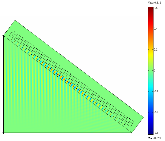
The ATR method requires the structure to be set close to the prism to get good coupling effect because the evanescent waves decay fast; however, while we are making use of the prism, the prism itself modifies the surface modes especially when it is very close to the structure. To get a satisfying experimental result, we need to optimize the airgap size to be able to record the mode while keeping the structure as far away from the prism as possible. In Fig. 3 the solid curves show the coupling effect at different air gap sizes at incident angle for the PC with corrugation layer of circular rods with diameter . You can see clearly in Fig. 3 that when the surface waves are excited, there is a very well defined dip in the reflection data. This is well shown for the distance of . In Fig. 4, one sees clearly that a surface wave is excited and almost no reflection is seen. Fig. 4 is an illustration of field distribution when a surface mode is excited, given by simulation. A surface wave with intensity much stronger than the incoming wave is seen along the corrugation layer of the PC. Actually the intensity of the surface wave is so strong that the reflected wave is hardly seen. This effect is observed as a dip in the reflection spectrum of the prism in our experiments (see Fig. 3 for ). The prism disturbs the coupling and the observed reflection dip position when the air gap is small; the dip converges to a constant frequency as the air gap increases. At larger incident angles, the coupling of the evanescent waves to surface waves is smaller and the dip position converges faster. This is because larger incident angle provides larger and thus larger absolute value of imaginary ; so the evanescent wave decays faster. For the surface corrugated PC, the ATR dip is still strong enough to be observed when the air gap between the prism and the surface of the structure is and is already converged except at incident angles near the critical angle. For a single layer of corrugation rods, the coupling is not as strong as for the full structure (PC and corrugation layer) case. To get good coupling, for the single corrugation layer, the air gap size is chosen to be .
Fig.2 shows the experimental results of the surface bands together with the calculation results for two different corrugation layers with and without PC. The solid points are the averaged dip frequencies over three measurements while the error bar on each point comes from the half width of the reflection dip, averaged over three different measurements. We can see that the experimental results are in good agreement with the calculated surface bands. However, at smaller incident angles, especially close to the critical angle, relatively large error bars are obtained. This is because the finite-width incident beam might not be fully reflected; some plane wave components propagate through the interface and change the coupling to the surface mode. Instead of a nice and sharp coupling dip, the coupling now is over a larger frequency range. That makes the half width of the dip larger. Also the evanescent wave decays slower at smaller and the coupling may not have converged yet at the largest air gap. So the overall experimental error is larger.
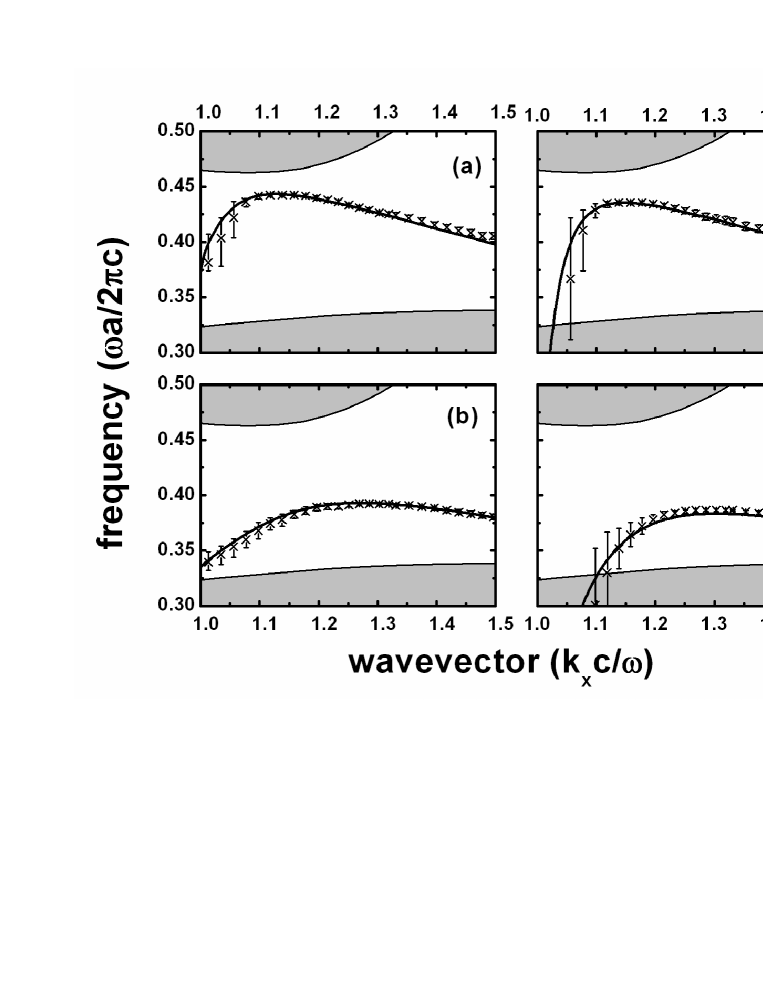
Simulations with a similar setup were done in FEMLAB and the results are shown in Fig.5. In the simulations, the source is a Gaussian beam normally incident at one side of a right-angled dielectric wedge. The rod array is set behind the hypotenuse of the wedge. The reflected power is obtained by integrating over the other side of the wedge. To get a coupling at different angles, the two acute angles of the wedge are changed so that the Gaussian beam is always normally incident on the wedge. Compared with experiments (Fig. 3), the reflection spectrum in simulations is always smoother. Also, the coupling can still be seen when the air gap is several centimeters large. The simulation results are in excellent agreement with the supercell calculations, as shown in Fig. 5.
In conclusion,we have investigated the excitation of surface waves on surface-corrugated PCs as well as single PC layers. ATR experiments and simulations have been done to excite different surface modes and the dispersion relations have been obtained, both being in good agreement with numerical calculations using the plane wave expansion method and the supercell method.
We gratefully acknowledge the support of Ames Laboratory, which is operated by Iowa State University under contract No. W-7405-Eng-82, EU projects PHOREMOST, METAMORAHOSE and DARPA contract No. HR0011-05-C-0068. This work was supported by the AFOSR under MURI grant FA9550-06-1-0337.
References
- (1) See, for example, Photonic Band Gap Materials, ed. by C. M. Soukoulis (Kluwer, Dordrecht, 1996); Photonic Crystals and Light Localization in the 21st Century, ed. by C. M. Soukoulis (Kluwer, Dordrecht, 2001).
- (2) J. D. Joannopoulos, R. D. Meade, J. N. Winn, Photonic Crystals: Molding the Flow of Light (Princeton University Press, Princeton, NJ, 1995).
- (3) W. M. Robertson and M.S. May, ”Surface electromagnetic wave excitation on one-dimensional photonic band-gap arrays”, Appl. Phys. Lett. 74, 1800 (1999).
- (4) J. M. Elson and P. Tran, ”Coupled-mode calculation with the R-matrix propagator for the dispersion of surface waves on a truncated photonic crystal”, Phys. Rev. B 54, 1711 (1996).
- (5) F. Ramos-Mendieta and P. Halevi, ”Surface electromagnetic waves in two-dimensional photonic crystals: Effect of the position of the surface plane”, Phys. Rev. B 59, 15112 (1999).
- (6) W. M. Robertson, G. Arjavalingam, R. D. Meade, K.D. Brommer, A. M. Rappe, and J. D. Joannopoulos, ”Observation of surface photons on periodic dielectric arrays”, Opt. Lett. 18, 528 (1993).
- (7) Y. A. Vlasov, N. Moll, and S. J. McNab, ”Observation of surface states in a truncated photonic crystal slab”, Opt. Lett. 29, 2175 (2004).
- (8) P. Kramper, M. Agio, C. M. Soukoulis, A. Birner, F. Muller, R. B. Wehrspohn, U. Gosele, and V. Sandoghdar, ”Highly Directional Emission from Photonic Crystal Waveguides of Subwavelength Width”, Phys. Rev. Lett. 92, 113903 (2004).
- (9) Esteban Moreno, F. J. Garcia-Vidal, and L. Martin-Moreno, ”Enhanced transmission and beaming of light via photonic crystal surface modes”, Phys. Rev. B 69, 121402 (2004).
- (10) I. Bulu, H. Caglayan, and E. Ozbay, ”Beaming of light and enhanced transmission via surface modes of photonic crystals”, Opt. Lett. 30, 3078 (2005).
- (11) K. M. Ho, C. T. Chan, and C. M. Soukoulis, ”Existence of a photonic gap in periodic dielectric structures”, Phys. Rev. Lett. 65, 3152 (1990).
- (12) F. Ramos-Mendieta and P. Halevi, “Surface modes in a 2D array of square dielectric cylinders”, Solid State Commun. 100, 311 (1996).
- (13) H. Raether, Surface Plasmons on Smooth and Rough Surfaces and on Gratings (Springer-Verlag, Berlin 1988).