A microscopic description of light induced defects in amorphous silicon solar cells
Abstract
Using a combination of quantum and classical computational approaches, we model the electronic structure in amorphous silicon in order gain understanding of the microscopic atomic configurations responsible for light induced degradation of solar cells. We demonstrate that regions of strained silicon bonds could be as important as dangling bonds for creating traps for charge carriers. Further, our results show that defects are preferentially formed when a region in the amorphous silicon contains both a hole and a light-induced excitation. These results agree with the puzzling dependencies on temperature, time, and pressure observed experimentally.
pacs:
PACS: 71.23.An, 61.43.Dq,72.10.FkDespite great promise as an inexpensive and efficient solar cell materialShah et al. (1999), hydrogenated amorphous silicon(a-Si:H) is severely limited by the Staebler-Wronski effect (SWE)Staebler and Wronski (1977), in which the efficiency is degraded by 25-30% within a few hours of exposure to light. While there is a strong consensus Stutzmann et al. (1985) that unsaturated (dangling) silicon bonds play an important role in the SWE by acting as charge traps, it is also clear that they cannot explain the entire effect Fritzche (2001). In fact, the photoconductivity can vary by more than a factor of ten at the same density of dangling bondsShimizu (2004).
In experiments, it has been observedBoland and Parsons (1992); Cody et al. (1981); Sriraman et al. (2002) that the quality of the random bond network of amorphous silicon is crucial to creating a high-quality sample. Large amounts of hydrogen are used, not to saturate dangling bonds, but to reduce the number of strained bonds. To date, however, it is unclear how this information about the deposition process relates to light-induced degradation, primarily because it is unfeasible to isolate individual defects in the amorphous material for study. Because of this, after 30 years of intense research aimed at understanding and mitigating this relatively straightforward macroscopic effect, a complete microscopic explanation for the performance degradation remains obscure.
In this Letter, we investigate the effect of the silicon bond network on the formation of charge carrier traps. Using a combination of classical force fields, density functional theory, and quantum Monte Carlo methods, we have sampled the space of random networks through bond switches, in which two silicon atoms exchange neighbors. Our calculations demonstrate that bond switches can create dangling bonds and they also can create regions of strained bonds that trap holes. These defects are preferentially formed when a region contains both a hole and an excitation. We show that a new picture of the SWE emerges from these results that is able to accomodate the characteristic dependencies on temperature, pressure, and time observed in experiments.
We have used a set of methods that increase in accuracy and computational expense. There is filtering done at each stage to ensure that the higher accuracy techniques are used only for potentially interesting samples of a-Si. First the WWWWooten et al. (1985) process using the KeatingKeating (1966) potential is performed, which filters the large space of all bond networks to a set of amorphous low-energy networks. Each low-energy network is then perturbed by a single bond switch, and these new networks are again filtered based on their energy. These sets of bond networks are then passed to DFT using the SiestaSoler et al. (2002) program, where the geometries are optimized, which can potentially break bonds. The hole trap depth is then obtained by calculating the difference in ionization energies between the low-energy network and its perturbations, i.e., . Networks with large trap depths are then singled out for analysis. We use VASPKresse and Furthmüller (1996) with the dimer methodHenkelman and Jonsson (1999) and nudged elastic band methodHenkelman et al. (2000) to find the transition state between the two bond networks for the ground and positively charged states. Finally, diffusion Monte Carlo(DMC)Foulkes et al. (2001) using the QWalkWagner et al. (2007) program was used to evaluate the transition barrier in the ground, positively charged, excited neutral, and excited positively charged states. This approach has been carried out for both 64-atom and 216-atom periodically repeated cells. The distributions are in agreement for both sizes. Because of the cost of finding many transition states and performing DMC calculations, we calculated only a few transition states in DFT on 216-atom cells, to confirm agreement with the 64-atom cells. The DMC results were all on 64-atom cells. All parameters were carefully checked for convergence111Energies were calculated within SIESTA with a DZP basis, 300 meV energy shift, and PBE functional. VASP calculations used a 245 eV energy cutoff, ultrasoft potentials, and PW-91 functional. DMC calculations used a Slater-Jastrow trial function with the one-particle orbitals from SIESTA with a TZTP basis, variance-minimized Jastrow coefficients, and a timestep of 0.05 Hartrees-1.

The statistical nature of this search is particularly crucial: unlike a perfect crystal, in an amorphous material a single periodically repeated simulation cell is not necessarily representative of the entire phase space. Thus, we perform all possible bond switches for six independent a-Si samples containing 216 atoms and twenty samples containing 64 atoms. There are hundreds of possible switches in each sample, of which we keep those that increase the energy less than 1.3 eV in our model. The results presented here thus are statistical, deriving from the analysis of hundreds of computational samples; we present representative examples to simplify the discussion, but the trends discussed throughout this work apply to the entire computational set.
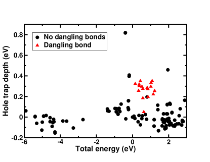
After the classical model/DFT minimization procedure, we analyze the electronic states to determine which network structures are hole traps/electron traps/low-energy absorbers (Fig 1). In our calculations, approximately 1-2 bond switches/nm3 change the electronic levels significantly from the reference structure, producing both electron and hole traps, as well as absorption at lower energy than the nominal 1.8 eV gap of amorphous silicon. We focus on the hole traps, since hole transport is the limiting factor in a-Si solar cells.
While the classical model used cannot break bonds, upon relaxation within DFT we find several instances where dangling bonds are formed, along with a complementary silicon atom with five bonds (a floating bond). A single bond switch is sufficient to form these dangling bond/floating bond pairs at either side of the switch, which results in a separation of approximately 1 nm, and only slightly higher energy (around 0.1 eV) than the original structure. This is similar in concept to the results of Biswas et al.Biswas et al. (2002) using a simpler tight-binding treatment of the electrons.
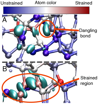
Surprisingly, however, we find that the deepest traps are not dangling bonds. To help understand why, we investigate two representative samples shown in Figure 2. The presence of the dangling bond (Figure 2A) allows nearby bonds to relax, since there are only three constraints on the 3-fold coordinated atom. A hole would then be forced to localize on the one atom, which is energetically less favorable due to an increase in the kinetic energy. The same reasoning holds true for a fully saturated but highly strained atom, as can be seen by the fact that the hole state does not localize on the highest strained atom in Figure 2B. On the other hand, a group of two to four strained atoms allow the hole to be less confined, while still binding a valence electron much more weakly (and thus binding a hole more strongly) than unstrained atoms. The hole is localized, so this state is a hole trap. The region of strained bonds is a stronger trap because of quantum confinement of the hole.

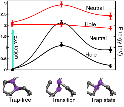
These results establish that strained regions of silicon atoms could be as important as dangling bonds for hole transport in amorphous silicon and that these defects can be created by a single bond switch. We now turn to the mechanism in which these bond switches can occur, which requires detailed analysis of the reaction pathway. Reaction barriers are well-known to be poorly described by density functional theory; one must employ a more accurate first principles method for a reliable descriptionGrossman and Mitas (1997). Thus, we use DFT to obtain the reaction path on 64-atom samples using the dimer methodHenkelman and Jonsson (1999), and then evaluate energy differences along the path using the highly accurate fixed node DMC method. The DMC barriers differ from DFT by up to 50%, which is enough to change the picture significantly, so the more accurate calculation is necessary in this case.
There are several potential light-induced events that may cause a bond switch. One is the collision and recombination of an electron and hole, which effectively locally heats the bond network, enabling the large ground-state barrier to be overcome. This mechanism is not supported by the high barrier and large energy cost in the ground state (Figure 3). Another possibility is through a light-induced electronic state other than the ground, neutral state. For this possibility, there are three major states: a hole, an electron, and an excited state, any two of which can potentially exist simulaneously in a region. Since holes are the slowest charge carriers, taking around 250 ns to exit a 500 nm deviceLuque and Hegedus (2003), they have the highest density of the three states. The second most numerous state is the excited state, which has a lifetime of around 10 nsKanemitsu et al. (2002). Finally, the electron exits a 500 nm device in around 1 nsLuque and Hegedus (2003), so it is the most sparse. The following analysis does not depend strongly on the actual lifetimes; only on their ordering.
If a hole happens to be in the region and the product bond configuration is a hole trap compared to the initial configuration, the energy difference between configurations decreases by the difference in ionization energies, which can be around 0.1-0.7 eV according to our calculations. The presence of a hole therefore preferentially forms hole-attracting bond networks; however, the reaction barrier to forming such networks is still substantial (Figure 3). One can imagine two further modifications to the electronic state–first, the system could attract a second hole, which is not favored electrostatically and in our calculations does not decrease the barrier very much, or second, the system could absorb a photon, exciting the unpaired electron.
When the unpaired electron is photoexcited, a single bond can lose one electron from the hole and have the other excited to an anti-bonding state from the excitation, which allows a bond to break and switch. In the case presented here in Figure 3, which is not unique in our samples, the energy ordering changes and the barrier is reduced to zero. Thus, when a hole is in a region that has the potential to change to a hole trap, and the region then absorbs a photon, a hole trap is formed with no barrier and a reduction in energy. When the excitation dissociates or decays, the energy ordering returns to the original condition and the barrier reappears.

These calculations lead us to the following potentially important mechanism in the SWE. A hole travels through a-Si slowly. While it is in a region, bond network changes with hole traps become more energetically favorable, but there is still a large barrier for the bond switch necessary to change the bond network. If that region happens to absorb a photon, the barrier to switch bonds is zero or nearly so, and the network with a hole trap is lower in energy. The system then performs the bond switch, which leads to a hole trap state.
This explanation of the SWE has several implications about the macroscopic behavior of a-Si, which can be validated by comparing to experiment. We have shown that bond switches can form dangling bonds, so experiments that measure the number of dangling bonds increasing with the decrease in solar cell efficiency are consistent with our results. In our picture, however, the dangling bonds are not the only hole traps. This is also in agreement with the observation that the number of dangling bonds can vary by a factor of ten and still have the same efficiency in the same sampleShimizu (2004). Furthermore, since strained silicon bonds are the major cause, our picture predicts a reduction in the SWE under a decrease in hydrostatic pressure, since the bonds are then able to relax. Dangling bonds, on the other hand, are less affected by a change in pressure, since the lone electron is still present. This provides a way of gauging the relative importance of the two types of defects. In experiments on light soaking, a slight increase in the volume of the sample is observedSakamoto et al. (2000), which in our picture is due to an increase in strain. It has also been observedWehrspohn et al. (2000); Crandall (1991) that if one removes the strain due to deposition, the SWE is reduced.

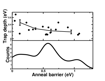
As an advantage of taking a statistical approach, we have the opportunity to compare the distribution of anneal barriers and trap depth. On 19 hole traps, the depth of the trap is anticorrelated with the anneal barrier, and the distribution of anneal barriers has a wide peak at around 0.70 eV (Figure 4). This anticorrelation is well-known in experiment; that is, traps formed at low temperatures are deeper, and a very similar distribution of anneal energies explains the temperature dependence of the SWEZhang et al. (1994).
Based on our simulations, one can develop a simple rate model for the creation of traps. Our results show that the barrier to create a hole trap is zero when a hole and an excitation collide, so , where is the density of defective regions, is the concentration of excited states, and is the concentration of holes. It is generally accepted that there is a concentration of holes proportional to , where is the flux of photons. Furthermore, the probability that a photon is absorbed by a region that is not defective is proportional to . Therefore, the creation rate for a simultaneous hole/photon is , which has the solution observed in experiment. Since the barrier is often nearly zero with a hole and excitation present, this analysis suggests that the defect creation rates in light would be nearly the same at all temperatures, which is the case in experimentStradins and Fritzsche (1996), but difficult to explain using a model that depends soley on diffusion of defects.
This picture opens several avenues for mitigation of the SWE. One is to redesign deposition processes to reduce the internal stress in the thin film, which reduces the number of hole traps. In the same vein, nanoscale features in the material that allow stress to be relieved could largely mitigate the SWE. An opposite strategy is to increase the rigidity of the bond network to prevent bond switches from happening in the first place; for example, by embedding nanocrystals in the materialZhang et al. (2006). Finally, in our description of the SWE the reaction is driven by an excitation combined with a hole that reverses the energy ordering of the defect-free and defective states. If a catalyst is introduced that reduces the ground state barrier, the defective bond network that is higher energy in the ground state can relax into the defect-free network at a lower than operating temperature, thus mitigating the SWE.
We have found that holes are trapped by both strained silicon bonds and dangling bonds and provided a simple and plausible mechanism in which the traps can form. The depth of the hole traps is determined by a balance between quantum confinement of the hole and the amount of strain in the bond, for which accurate treatment of electrons is particularly crucial. The strained bond/bond switch explanation of the SWE suggests further exploration in experiments aimed at mitigating the SWE. Advances in this area have the opportunity of increasing the efficiency of amorphous silicon based solar cells by 30% or more, which is a significant step towards creating a less expensive alternative to higher efficiency crystalline silicon cells.
Acknowledgements.
This work was performed under the auspices of the National Science Foundation by the University of California Berkeley under Grant No. 0425914.References
- Shah et al. (1999) A. Shah, P. Torres, R. Tscharner, N. Wyrsch, and H. Keppner, Science 285, 692 (1999).
- Staebler and Wronski (1977) D. Staebler and C. Wronski, Appl. Phys. Lett. 31, 292 (1977).
- Stutzmann et al. (1985) M. Stutzmann, W. Jackson, and C. Tsai, Phys. Rev. B 32, 23 (1985).
- Fritzche (2001) H. Fritzche, Annu. Rev. Mater. Res. 31, 47 (2001).
- Shimizu (2004) T. Shimizu, Jpn. J. of Appl. Phys. 43, 3257 (2004).
- Boland and Parsons (1992) J. Boland and G. Parsons, Science 256, 1304 (1992).
- Cody et al. (1981) G. Cody, T. Tiedje, B. Abeles, B. Brooks, and Y. Goldstein, Phys. Rev. Lett. 47, 1480 (1981).
- Sriraman et al. (2002) S. Sriraman, S. Agarwal, E. S. Aydil, and D. Maroudas, Nature 418, 62 (2002).
- Wooten et al. (1985) F. Wooten, K. Winer, and D. Weaire, Phys. Rev. Lett. 54, 1392 (1985).
- Keating (1966) P. N. Keating, Phys. Rev. 145, 637 (1966).
- Soler et al. (2002) J. M. Soler, E. Artacho, J. D. Gale, A. García, J. Junquera, P. Ordejón, and D. Sánchez-Portal, J. Phys. Cond. Matter 14, 2745 (2002), URL http://stacks.iop.org/0953-8984/14/2745.
- Kresse and Furthmüller (1996) G. Kresse and J. Furthmüller, Phys. Rev. B 54, 11169 (1996).
- Henkelman and Jonsson (1999) G. Henkelman and H. Jonsson, J. Chem. Phys. 111, 7010 (1999).
- Henkelman et al. (2000) G. Henkelman, B. P. Uberuaga, and H. Jónsson, The Journal of Chemical Physics 113, 9901 (2000), URL http://link.aip.org/link/?JCP/113/9901/1.
- Foulkes et al. (2001) W. M. C. Foulkes, L. Mitas, R. J. Needs, and G. Rajagopal, Rev. Mod. Phys. 73, 33 (2001).
- Wagner et al. (2007) L. Wagner, M. Bajdich, and L. Mitas, arXiv p. 0710.4361 (2007).
- Biswas et al. (2002) R. Biswas, B. Pan, and Y. Ye, Phys. Rev. Lett. 88, 205502 (2002).
- Tersoff (1988) J. Tersoff, Phys. Rev. B 38, 9902 (1988).
- Grossman and Mitas (1997) J. C. Grossman and L. Mitas, Phys. Rev. Lett. 79, 4353 (1997).
- Luque and Hegedus (2003) A. Luque and S. Hegedus, Handbook of Photovoltaic Science and Engineering (John Wiley and Sons, 2003), pp. 505–565.
- Kanemitsu et al. (2002) Y. Kanemitsu, S. Nihonyanagi, Y. Fukunishi, and T. Kushida, Phys. Stat. Sol. (a) 190, 769 (2002).
- Sakamoto et al. (2000) T. Sakamoto, N. Yoshida, T. Kishida, S. Nonomura, T. Gotoh, M. Kondo, A. Matsuda, T. Itoh, and S. Nitta, J. Non-Cryst. Solids 266-269, 481 (2000).
- Wehrspohn et al. (2000) R. B. Wehrspohn, S. C. Deane, I. D. French, I. Gale, J. Hewett, M. J. Powell, and J. Robertson, J. of Appl. Phys. 87, 144 (2000), URL http://link.aip.org/link/?JAP/87/144/1.
- Crandall (1991) R. S. Crandall, Phys. Rev. B 43, 4057 (1991).
- Zhang et al. (1994) Q. Zhang, H. Takashima, J.-H. Zhou, M. Kumeda, and T. Shimizu, Phys. Rev. B 50, 1551 (1994).
- Stradins and Fritzsche (1996) P. Stradins and H. Fritzsche, J. Non-Cryst. Solids 198-200, 432 (1996).
- Zhang et al. (2006) S. Zhang, X. Liao, L. Raniero, E. Fortunato, Y. Xu, G. Kong, H. Aguas, I. Ferreira, and R. Martins, Solar Energy Materials & Solar Cells 90, 3001 (2006).