Enhanced Ferromagnetic Stability in Cu Doped Passivated GaN Nanowires
Abstract
Density functional calculations are performed to investigate the room temperature ferromagnetism in GaN:Cu nanowires (NWs). Our results indicate that two Cu dopants are most stable when they are near each other. Compared to bulk GaN:Cu, we find that magnetization and ferromagnetism in Cu doped NWs is strongly enhanced because the band width of the Cu band is reduced due to the 1D nature of the NW. The surface passivation is shown to be crucial to sustain the ferromagnetism in GaN:Cu NWs. These findings are in good agreement with experimental observations and indicate that ferromagnetism in this type of systems can be tuned by controlling the size or shape of the host materials.
Dilute magnetic semiconductors (DMSs) have attracted wide interest recently because they possess both semiconducting and magnetic properties at the same time, thus suitable for spintronic applications. One of the major focus in this important research field is to produce DMSs with Curie temperatures () at or above room temperature. It has been predicted that the use of wide band-gap semiconductors, e.g., GaN, as the host material for DMSs can lead to high Dietl2000 . However, experimental studies on transition-metal (TM)-doped bulk GaN have led to conflicting results. For example, some experiments have shown the existence of ferromagnetism in Ga1-xMnxN but with varying between 8 K Sarigiannidou2006 and 904 K Sonoda2002 at . In contrast, a magneto-optical study Ando2003 suggested that Ga1-xMnxN is paramagnetic. Theoretical studies also show that the magnetic properties of bulk Ga1-xMnxN is quite unique: depending on the Mn concentration, carrier density, and pressure, it can change from ferromagnetism to antiferromagnetism Dalpian2005 ; Dalpian2006 .
Recently, Wu et al. Wu2006 predicted that two Cu ions in a configuration about 6.2 Å from each other in bulk GaN are coupled ferromagnetically with the total moment 2 /Cu. Subsequently, room temperature ferromagnetism was found in Cu-implanted GaN samples, although with a much smaller saturation magnetization (from 0.01 to 0.27 /Cu), and the results are very sensitive to the annealing temperature Lee2007 ; Seipel2007 . A more recent calculation by Rosa and Ahuja Rosa2007 points out that the ferromagnetic coupling in bulk GaN:Cu is much weak than expected from previous calculation Wu2006 because the magnetic moment on Cu is very sensitive to the Cu-Cu distance; it becomes much smaller when Cu-Cu becomes nearest neighbor. However, a recent experimental study by Seong et al. reported that room temperature ferromagnetism can be achieved in Ga1-xCuxN nanowires (NWs) synthesized in a chemical vapor transport system under flow of NH3 and the saturation magnetic moment is significantly higher than that in bulk GaN (1.00 /Cu at 5 K) Seong2007 . The dramatically different saturation magnetic moment of Cu in bulk GaN and GaN NWs suggest that the magnetic behavior of Cu doped GaN could be manipulated by tuning the size or shape of host. However, the mechanism of the enhanced magnetic coupling in GaN:Cu NWs is not known, including what is the effect of the surface passivation in the NWs.
In this Letter, we perform a comprehensive first principles study to understand the structural and magnetic properties of Cu doping in bulk GaN and GaN NWs. Both bare and passivated GaN NWs are studied. Our first-principles spin-polarized density functional theory (DFT) calculations were performed on the basis of the projector augmented wave method PAW encoded in the Vienna ab initio simulation package VASP using the generalized-gradient approximation (GGA) Perdew1996 and the plane-wave cutoff energy of 400 eV. For relaxed structures, the atomic forces are less than 0.02 eV/Å.
For bulk GaN, the optimized wurtzite lattice constants are a Å and c Å with the internal parameter u= (experimental values: a Å, c Å, and u=). The calculated band gap for bulk GaN is 1.72 eV. The GaN NWs are orientated along the [0001] direction with a diameter about 1 nm, as shown in Fig. 1(a) and (b). For passivated NWs, pseudo-hydrogen is used to saturate the dangling bond of the NW surface. In the simulation, the NW axis is along the direction, and the lateral supercell size is chosen so that the closest distance between two neighbor NWs is larger than 8 Å. After optimization, the diameters of the GaN NWs become slightly smaller, and consequently, to minimize the strain, the lattice constant is increased by 0.018 Å and 0.046 Å for passivated and bare GaN NWs, respectively, as in the case of bare ZnO NWs Xiang2006 . Both bare and passivated NWs are found to have a direct bang gap (1.67 eV and 3.25 eV, respectively) at . The small band gap of the bare wire is due to the formation of surface defect levels. In case of Cu doping in NWs, we use a supercell with a k-mesh. For comparison, Cu doping in bulk GaN is also studied by using a supercell (shown in Fig. 1(e)) with a k-mesh. The lattice constants of the doped systems are fixed to those of the undoped hosts since substitutional Cu changes only marginally the lattice constant Wu2006 ; Seipel2007 .
To compare the dopability of Cu in bulk GaN and GaN NWs and identify stable dopant position, we first calculate the formation energy of Cu substitution for Ga in GaN host as
| (1) |
where is the total energy of the doped system, denotes the total energy of the GaN host for the same supercell in the absence of the defect, and are the chemical potential for Ga and Cu, respectively. We note that the absolute formation energy depends on and . However, it is sufficient to calculate for the purpose of comparing the relative stability of Cu in GaN host. For a NW as shown in Fig. 1(a) and (b), there are three inequivalent Ga positions, i.e., A, B, and C. In all cases, we confirm that Cu will not form AX center in GaN due to the delocalization of the Cu 3d related defect bands. Our results are reported in Table. 1. For bare GaN NW, we find that the formation energy of CuGa is smaller than that in bulk GaN, because CuGa can relax more easily in the NW than in the bulk. The lowering of the formation energy is most dramatic at the surface of the NW, where the formation energy is about 0.96 eV smaller. For the passivated GaN NW, we find that the formation energy of CuGa is about 0.3 eV larger than that in bulk GaN and is most stable at the A site. This result follow the general trends observed in nanocrystal quantum dots Li2008 suggesting that the increased formation energy for this non-isovalent dopants is mainly due to the quantum confinement-induced band gap increase, but not sensitive to the shape of the quantum structure. The above results show that the doping ability of Cu in GaN NW depends sensitively on the surface termination of the NW. We also find that in all cases with an isolated Cu atom in GaN hosts, the total magnetic moment is 2 and the local moment on Cu is about 0.65 due to the strong Cu 3d and N 2p hybridization Wu2006 .
Experimentally, the valence state of Cu in Cu doped GaN NW is found to be close to that of Cu in CuO Seong2007 . To confirm this theoretically, we calculate the charge tranfer in Cu doped NWs using atoms in molecules (AIM) theory Bader . We find that the valence state of Cu dopant in bare (passivated) GaN NW is about 0.84 (0.88). For CuO and Cu2O, the calculated Cu valence state is 0.99 and 0.55, respectively. So, the valence state of Cu dopant in GaN NW is indeed close to that in CuO. The calculated valence state is not close to the nominal value due to the strong covalency in the system. The results also indicate that Cu occupies Ga site in the experimental sample Seong2007 .
To investigate the interaction between Cu dopants in GaN NWs, we substitute two Ga atoms with two Cu atoms. The most stable configuration of two Cu atoms in GaN NWs is shown in Fig. 1. We can see that two Cu atoms tend to be next to each other, i.e., they are bonded to the same N atom. This is due to the strong bonding interaction between Cu 3d states. In case of passivated NW, both Cu atoms occupied A positions. In contrast, these Cu atoms occupied C positions for the bare GaN NW case. This is understandable since an isolated Cu atom prefers to occupy the C (A) position in case of bare (passivated) GaN NW.
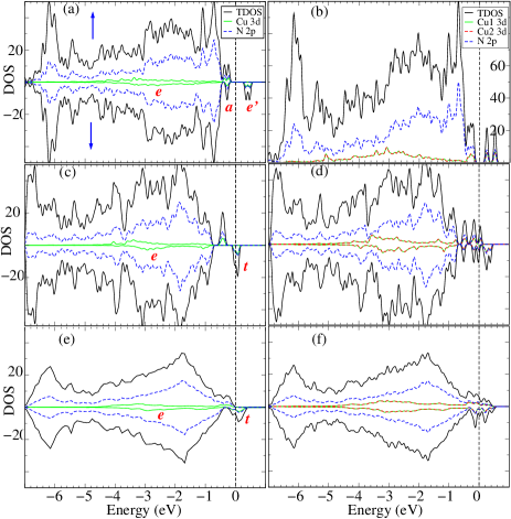
The spin exchange interaction between Cu 3d moments in GaN NWs is studied through calculating different spin states, i.e., ferromagnetic (FM) and antiferromagnetic (AFM) states. In case of Cu doped passivated GaN NW (Fig. 1(d)), the FM state with a total moment 2.8 is more favorable over the AFM state by 90 and 31 meV for the unrelaxed and relaxed structures, respectively. Surprisingly, for the doped bare GaN NW as shown in Fig. 1(c), it is a non-magnetic semiconductor with a gap of 0.44 eV within the d bands. To probe the origin of the different nature of magnetism in these two cases, we plot the density of states (DOS) in Fig. 2. To facilitate the analysis, the DOSs of the systems with an isolated Cu dopant are also shown. In both cases, we can see that there is a band gap in the spin up component. In case of the passivated NW, the spin down orbitals (In the crystal field of a wurtzite system, 3d orbitals are splitted into low-lying two-fold states and three nearly degenerated orbitals) are partially occupied. However, when a Cu atom occupies the surface position [position C in Fig. 1(a)] of the bare GaN NW, the different crystal field arising from a missing neighbor N atom at the surface will split the orbitals into a low-lying one-fold and a high-lying two-fold sets. The presence of the band gap is consistent with the stability of the surface Cu atom. When the two Cu dopants are next to each other [Fig. 1(c)], the coupling between two Cu -derived orbitals will result in a splitting between the bonding and anti-bonding orbitals. Since the distance between two Cu atoms in bare NW is only 2.93 Å (the Cu-Cu distance in bulk GaN and passivated GaN NW are 3.13 Å and 3.12 Å respectively), the splitting will be larger than the spin exchange splitting, resulting in the low spin non-magnetic state. Similar results are observed in GaN:Mn, where pressure or surface strain can turn the system from a high-spin to a low-spin configuration, diminish the ferromagnetism Dalpian2005 ; Wang2004 . Our calculations reveal that passivation of the surface is crucial in this system to obtain ferromagnetism for Cu doped GaN NWs. It is noted that previous theoretical studies focused only on TM (Mn Wang2005A and Cr Wang2005B ) doped GaN bare NWs. In addition, the coupling between a pair of Cr atoms substituted in unsaturated GaN nanoholes was found to be FM Wang2007 .
| site A | site B | site C | |
|---|---|---|---|
| Bare NW | 3.05 | 3.27 | 2.37 |
| Passivated NW | 3.52 | 3.68 | 3.52 |
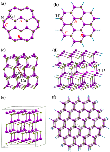
To compare the different magnetic behavior of Cu doping in bulk GaN and GaN NW, we also study the Cu-Cu interaction in bulk GaN. First, we find that Cu dopants in bulk GaN also tend to be nearest neighbor. The most favorable configuration is that two Cu atoms occupy the in-plane nearest neighbor positions [positions 1 and 2 in Fig. 1(e)] with a magnetic moment of 0.6 /Cu. However, the energy difference between the FM and the AFM state in this configuration is only meV (the value for the unrelaxed structure is 10.5 meV), which is much smaller than that in passivated NW and in the case when the Cu-Cu distance is about 6.2 Å Wu2006 . In some other configurations, we find that the AFM state could be even more stable than the FM state. For instance, if two Cu atoms occupy positions 1 and 3 [Fig. 1(e)], the FM state has higher energy by 41 meV. These results indicate that FM in Cu doped bulk GaN is not robust, which is consistent with experimental observations and the recent calculations of Rosa and Ahuja Rosa2007 .
To unravel the origin of the different behavior of Cu dopants in bulk GaN and passivated GaN NWs, we illustrate the DOS of the orbitals near the fermi level in Fig. 3. For the isolated Cu dopant, the main difference between bulk GaN:Cu and GaN:Cu NW is that the band width of the states is smaller in NWs than that in bulk GaN (0.13 eV v.s. 0.53 eV) due to the quasi-1D nature of NWs. The DOSs for an isolated Cu in bulk GaN and GaN NWs resemble those shown in Fig. 3(a) and (d), respectively. When two Cu dopants are close to each other, the orbitals in the same spin will couple to each other, resulting in a low-lying bonding set and a high-lying anti-bonding one in the FM state, broadening the band. This stabilize the FM state over the AFM state due to the more occupation of the spin-down bonding orbitals than the anti-bonding state Dalpian2006 ; Sluiter2005 . However, it also increases the overlapping between the spin-up and spin-down bands, causing electron transfer from the spin-up states to spin-down states as shown in [Fig. 3(b) and (e)], reducing the magnetic moment. The transfer is large in bulk GaN than in GaN NW because the band width in bulk GaN is wider. The reduced magnetic moment further leads to a reduced exchange splitting and more charge transfer. The final DOSs of the FM state for two Cu atoms in bulk GaN is shown in Fig. 3(c). This explains why Cu-Cu pairs in bulk GaN has a very small magnetic moment when the Cu-Cu distance is small and why the magnetic interaction is weak in bulk GaN. This is because for bulk GaN:Cu, when Cu-Cu distance is small, the coupling between Cu orbital is large, but the magnetic moment is small. When the Cu-Cu distance is large, the magnetic moment is recovered, but the orbital coupling becomes small. On the other hand, the Cu orbital band width is much smaller in GaN NW, thus the charge transfer and reduction of magnetic moment is small in GaN:Cu NWs even when the Cu-Cu distance is small [Fig. 3(f)]. This explains why magnetization and ferromagnetism is enhanced in GaN:Cu NWs.
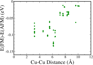
Due to the configurational entropy, Cu dopants might have many different configurations in GaN NWs under experimental growth condition. Here to examine the dependence of the magnetic properties on the configuration, we study all possible inequivalent configurations (102 configurations in total) of two Cu atoms in passivated GaN NW. To reduce the computational amount, no structural relaxation is performed. It turns out that in all cases, FM is always preferred over the AFM state, as shown in Fig. 4. Interestingly, the maximum magnitude of the energy difference occur at some configurations with the Cu-Cu distance about 6 Å, instead of the nearest neighbor configurations. This is because when the Cu-Cu distance is smaller than 6 Å the magnetic moment start to decrease, thus reducing the magnetic interactions, as discussed above. However, unlike in bulk GaN:Cu, the energy difference is still negative and large at nearest neighbor Cu-Cu distance. Thus FM in Cu doped passivated GaN NW is robust with respect to Cu configurations in GaN NWs.
In the experimental work by Seong et al. Seong2007 , the diameter of the GaN NW is larger than that of the NW we discussed above. Here to investigate the magnetic interaction between Cu dopants in larger GaN NWs, we also consider two Cu dopants in passivated GaN NW with a diameter about 1.6 nm, as shown in Fig. 1(f). From our calculation, the FM state is more stable by 75 and 54 meV than the AFM state for the unrelaxed and relaxed structures, respectively. So the change of exchange interaction between Cu atoms in GaN NW is not very significant when the diameter of the NW changes.
In summary, we explained why the ferromagnetism of GaN:Cu is enhanced in passivated GaN NWs. We show that due to the 1D nature of the NW, the band width of the Cu band is reduced, thus increases the magnetization. It is found that passivation of the nanowire surface has a significant impact on the substitutional position, and thus on the magnetic properties: For the bare GaN NWs, Cu tends to substitute Ga on the surface, and the strong direct interaction between two neighboring surface substitutional Cu atoms results in a non-magnetic semiconducting state. However, when the surface is passivated, Cu tends to substitute Ga inside the NW, and leads to ferromagnetism arising from the - exchange interactions. Our findings, thus, indicate that surface passivation of the NW is crucial to sustain the FM state.
This work is supported by the U.S. Department of Energy, under Contract No. DE-AC36-99GO10337. We thank Dr. Juarez L. F. Da Silva and Dr. Sukit Limpijumnong for useful discussions.
References
- (1) Dietl, T.; Ohno, H.; Matsukura, F.; Cibert, J.; Ferrand, D. Science 2000, 287, 1019.
- (2) Sarigiannidou, E.; Wilhelm, F.; Monroy, E.; Galera, R. M.; Bellet-Amalric, E.; Rogalev, A.; Goulon, J.; Cibert, J.; Mariette, H. Phys. Rev. B 2006, 74, 041306(R).
- (3) Sonoda, S.; Shimizu, S.; Sasaki, T.; Yamamoto, Y.; Hori, H. J. Cryst. Growth 2002, 237, 1358.
- (4) Ando, K. Appl. Phys. Lett. 2003, 82, 100.
- (5) Dalpian G. M.; Wei, S.-H. J. Appl. Phys. 2005, 98, 083905.
- (6) Dalpian, G. M.; Wei, S.-H.; Gong, X. G.; da Silva, A. J. R.; Fazzio, A. Solid State Commun. 2006, 138, 353.
- (7) Wu, R. Q.; Peng, G. W.; Liu, L.; Feng, Y. P.; Huang, Z. G.; Wu, Q. Y. Appl. Phys. Lett. 2006, 89, 062505.
- (8) Lee, J.-H.; Choi, I.-H.; Shin, S.; Lee, S.; Lee, J.; Whang, C.; Lee, S.-C.; Lee, K.-R.; Baek, J.-H.; Chae, K. H.; Song, J. Appl. Phys. Lett. 2007, 90, 032504.
- (9) Seipel, B.; Erni, R.; Gupta, A.; Li, C.; Owens, F. J.; Rao, K. V.; Browning, N. D.; Moeck, P. J. Mater. Res. 2007, 22, 1396.
- (10) Rosa, A. L.; Ahuja, R. Appl. Phys. Lett. 2007, 91, 232109.
- (11) Seong, H.-K.; Kim, J.-Y.; Kim, J.-J.; Lee, S.-C.; Kim, S.-R.; Kim, U.; Park, T.-E.; Choi, H.-J. Nano Lett. 2007, 7, 3366.
- (12) Blöchl, P. E. Phys. Rev. B 1995, 50, 17953; Kresse, G; Joubert, D. Phys. Rev. B 1999, 59, 1758.
- (13) Kresse, G; Furthmüller, J Comput. Mater. Sci. 1996, 6, 15; Phys. Rev. B 1996, 54, 11169.
- (14) Perdew, J. P.; Burke, K.; Ernzerhof, M. Phys. Rev. Lett. 1996, 77, 3865.
- (15) Xiang, H. J.; Yang, J. L.; Hou, J. G.; Zhu, Q. S. Appl. Phys. Lett. 2006, 89, 223111.
- (16) Li, J.; Wei, S.-H.; Li, S. S.; Xia, J. B. Phys. Rev. B 2008 77, 113304.
- (17) Bader, R. F. W. Atoms in Molecules-A Quantum Theory (Oxford University Press, Oxford, 1990).
- (18) Wang, Q.; Sun, Q.; Jena, P.; Kawazoe, Y. Phys. Rev. Lett. 2004, 93, 155501.
- (19) Wang, Q.; Sun, Q.; Jena, P. Phys. Rev. Lett. 2005, 95, 167202.
- (20) Wang, Q.; Sun, Q.; Jena, P.; Kawazoe, Y. Nano Lett. 2005, 5, 1587.
- (21) Wang, Q.; Sun, Q.; Jena, P.; Kawazoe, Y. Phys. Rev. B 2007, 75, 075312.
- (22) Sluiter, M. H. F.; Kawazoe, Y.; Sharma, P.; Inoue, A.; Raju, A. R.; Rout, C.; Waghmare, U. V. Phys. Rev. Lett. 2005, 94, 187204.