Low voltage control of ferromagnetism in a semiconductor p-n junction
pacs:
75.50.Pp, 81.05.Ea, 85.75.HhThe concept of low-voltage depletion and accumulation of electron charge in semiconductors, utilized in field-effect transistors (FETs), is one of the cornerstones of current information processing technologies. Spintronics which is based on manipulating the collective state of electron spins in a ferromagnet provides complementary technologies for reading magnetic bits or for the solid-state memories.Wolf et al. (2001) The integration of these two distinct areas of microelectronics in one physical element, with a potentially major impact on the power consumption and scalability of future devices, requires to find efficient means for controlling magnetization electrically. Current induced magnetization switching phenomena Ralph and Stiles (2008) represent a promising step towards this goal, however, they relay on relatively large current densities. The direct approach of controlling the magnetization by low-voltage charge depletion effects is seemingly unfeasible as the two worlds of semiconductors and metal ferromagnets are separated by many orders of magnitude in their typical carrier concentrations Marder (2000). Here we demonstrate that this concept is viable by reporting persistent magnetization switchings induced by short electrical pulses of a few volts in an all-semiconductor, ferromagnetic p-n junction.
To establish the physics behind this main result of our work, we organized the paper as follows: After describing the basic structure of the device we present direct electrical measurements of simultaneous charge depletion and ”depletion” of the magnetization, i.e. of the shifts in the ferromagnetic Curie temperature, by applying a few volts. This provides the ultimate test of the ability to manipulate the magnetic state by low-voltages. We point out that the method we introduce for accurate electrical measurement of in the microdevice is essential as standard magnetometry is not feasible at these small sample dimension. We then proceed by discussing the nature of the magnetotransport responses in our system. They are remarkable on their own for their large magnitude and voltage-dependence and provide the means for detecting the magnetic moment reorientations induced by low-voltage pulses, again by electrical measurements. The main body of the paper is devoted to presenting and discussing the phenomenology of the electrically controlled magnetization switchings measured as a function of the magnitude and angle of the external magnetic field. The microscopic physical interpretation of our experiments, based on semiconductor theory modelling, is discussed in the concluding paragraphs.
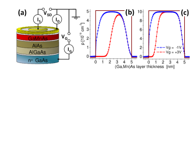
The schematic cross-section of the III-V heterostructure used in our study is shown in Fig.1(a). It is a semiconductor p-n junction FET specially designed to accommodate ferromagnetism in the p-type region and its efficient depletion by low voltages. From the top, the structure comprises a 5 nm thick approximately 2.5% Mn-doped GaAs capped by 2 nm of undoped GaAs to prevent oxidation of the underlying transition metal doped semiconductor film. These two top layers were grown by low-temperature molecular-beam-epitaxy (MBE) to avoid Mn precipitation. The 2.5% doping was chosen to pass the insulator-to-metal transition threshold which for the moderately deep MnGa acceptor is between 1-2% and to achieve robust ferromagnetic state with Curie temperature K, while still minimizing the number of unintentional interstitial-Mn impurities.Matsukura et al. (2002); Jungwirth et al. (2006, 2007) (The interstitial Mn is highly mobile at the growth temperature and its diffusion into the p-n junction would result in detrimental leakage currents.) The Curie temperature measured by SQUID in an unpatterned piece of the wafer is comparable to maximum ’s achieved at the same Mn-doping in thicker films, indicating a very good quality of our ultra-thin ferromagnetic semiconductor epilayer.
The n-type gate electrode is formed by a highly Si-doped ( cm-3) GaAs grown by high-temperature MBE. The large electron doping is required in order to achieve appreciable and voltage dependent depletion of the ferromagnetic p-region with hole doping cm-3. The built-in electrostatic barrier due to the depletion effect at the p-n junction is further supported by inserting an undoped AlGaAs spacer with a large conduction band off-set to the n-type GaAs; for the same reason a large valence band offset AlAs spacer is placed next to the p-type (Ga,Mn)As.
Self-consistent numerical simulations,silvaco shown in Fig. 1(b), confirm that sizable depletions are achievable by gating our heterostructure with less than 4 Volts. Measurements discussed below were done at voltages between V (forward bias) to V (reverse bias) for which the leakage currents between the n-GaAs gate and p-(Ga,Mn)As channel were more than two orders of magnitude smaller than the channel currents. The (Ga,Mn)As channel was lithographically patterned in a low-resistance Corbino disk geometry with the inner contact radius of 500 m and the outer radius of 600 m.
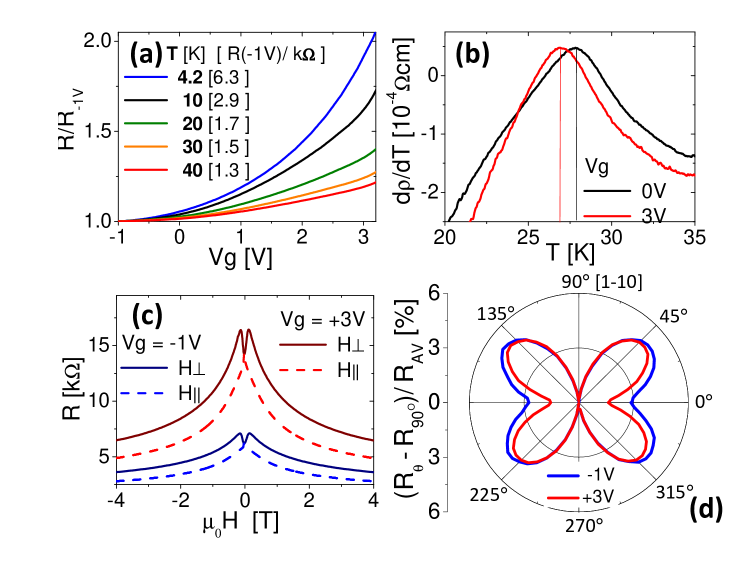
In Fig. 2(a) we plot the measured channel resistances vs. gate-voltage at temperature 4-40 K. Both at low temperatures and near we observe a marked increase of the channel resistance at positive voltages. It is consistent with the depletion of the (Ga,Mn)As channel as predicted by the simulations in Fig. 1(b) and with the vicinity of the metal-insulator transition which causes the superlinear increase of with . At 4 K, the increase of between -1 and +3 V is by more than 100%.
In Fig. 2(b) we show the voltage-dependence of the Curie temperature in the ferromagnetic p-n junction. Our measurement technique is distinct from previous studies which relied on approximate extrapolation schemes based on Arrot plot measurements at finite magnetic fields.Ohno et al. (2000); Chiba et al. (2006); Stolichnov et al. (2008) Recent observation and interpretation by the authors Novak et al. (2008) of the peak in the zero-field temperature derivative of the resistance at the Curie point in good quality (Ga,Mn)As materials has provided the tool for direct transport measurements of in microdevices without relying on any extrapolation schemes. In Fig. 2(b) we plot differentiated resistivity curves obtained in our device at -1 and +3 V. The data show a clear shift of the Curie temperature, i.e., the magnetization can be turned on and off in parallel with accumulating and depleting holes in the ferromagnetic semiconductor channel by biasing the p-n junctions with a few Volts.
Curie temperature variations provide the key physical demonstration of the low-voltage control of magnetization. Nevertheless, for most spintronic functionalities it is not required to destroy the ordered state of spins but only to change their collective orientation. We therefore focus on effects related to reorientations of the unit vector of the macroscopic moment. To avoid thermal fluctuations of the magnetization, all measurements are done far from the Curie point at 4 K.
In Fig. 2(c) we show magnetoresistance traces recorded during in-plane and perpendicular-to-plane sweeps of an external magnetic field, at gate voltages of -1 and +3 V. Apart from the negative isotropic magnetoresistance (IMR), the data indicate a remarkably large anisotropic magnetoresistance (AMR) effect which at saturation reaches %. (Note that AMR sensors fabricated in transition metal ferromagnets with AMR ratios of a few per cent McGuire and Potter (1975) marked the dawn of spintronics in the early 1990’s.) The resistance is larger for the perpendicular-to-plane magnetization orientation and the size of the effect is enhanced by depletion. The electrical response of our system to magnetization rotations is both large and tuneable by low gate voltages.
The magnetoresistance traces in Fig. 2(c) indicate that the film has a magnetic anisotropy favoring in-plane magnetization, which is overcome by an external field of approximately 150 mT. At weaker magnetic fields, magnetization switching effects are confined to the plane of the ferromagnetic film. The qualitative nature of the in-plane magnetic anisotropy landscape which determines the switching processes can be scanned in our Corbino microdevice by recording the AMR at a rotating in-plane saturation field. Unlike in the out-of-plane rotation AMR, contributions depending on the relative angle between the in-plane magnetization and current average out over the radial current lines. The in-plane AMR then depends purely on the angle between magnetization and crystallographic axes.Rushforth et al. (2007) It reflects therefore the same underlying symmetry breaking crystal fields as the magnetic anisotropy. The measurements, shown in Fig. 2(d), unveil a cubic anisotropy along the [110]/[10] crystal axes and an additional uniaxial term breaking the symmetry between the [110] and [10] directions. Although the specific responses to these symmetries can be very different for the AMR and for the magnetic anisotropy, the presence of the cubic and uniaxial AMR terms and their sensitivity to the gate voltage observed in Fig. 2(d) suggest that the in-plane magnetization orientation itself can be switched at weak magnetic fields by the low voltage charge accumulation or depletion.
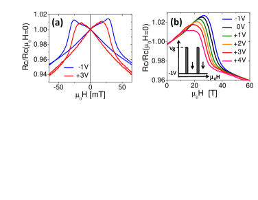
A variable width of hysteretic magnetization loops measured at different constant gate voltages, shown in Fig.3(a), is the prerequisite for observing electrically assisted magnetization switchings. Note that electrical measurements of magnetization reorientations utilized in Figs. 3 and 4 are facilitated in our system by the IMR which responds to abrupt changes of the total magnetic induction upon a 180∘ reversal, and by a combined effect of the IMR and of the AMR for intermediate switchings by less than 180∘. The amplitude of the AMR and the IMR contributions are similar in our experiments. The switchings by short low-voltage pulses are demonstrated in Fig. 3(b) and analyzed in detail in Fig. 4. The experiments were performed at constant field-sweep rate of 0.1 mT per second starting from negative saturation field of 1 T. The gate voltage was set to a base value of -1 V and then after each measurement step spanning 1 second we applied a 10 ms voltage pulse of a fixed magnitude and then returned to the base voltage. The technique allows us to demonstrate magnetic response to short electric pulses and the persistence of induced reorientations of the magnetization vector. It also removes potentially obscuring variations among the resistance traces in regions away from magnetization switchings which are caused by different slopes of the negative IMR at different gate voltages.
In Fig. 3(b) we compare measurement with no pulses (constant -1 V gate voltage) and data acquired at 0 to +4 V peak voltages. The field was swept along the [10] crystal direction (, where is the in-plane field angle measured from the [110] direction). As argued in detail in Fig. 4 and confirmed by SQUID magnetization measurements on an unpatterned part of the wafer, [10] is the main magnetic easy axis. The negative IMR then allows us to observe the drop in corresponding to a 180∘ reversal from an antiparallel to a parallel configuration of field and magnetization and a corresponding increase of the magnetic induction. As the applied peak voltage increases, the magnetization reversals consistently shift to lower magnetic fields and the magnetization remains switched when the peak voltage pulse is turned off.
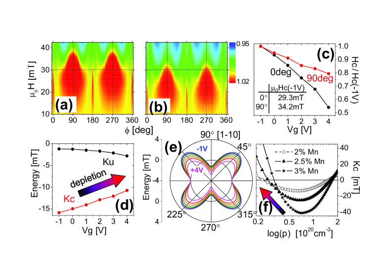
To discuss the detail phenomenology of these persistent low-voltage induced magnetization switchings we present in Figs. 4(a) and (b) field-sweep measurements at fixed field angles spanning the whole interval from 0 to 180∘ in 5∘ steps. In panels (a) and (b) we show color-maps of the resistance as a function of the field magnitude and angle for -1 V constant voltage and for the +3 V peak-voltage measurements, respectively. The main effect observed in these plots is the overall suppression of the magnitude of the switching fields by depletion. Additionally, the relative suppression is stronger at than at 90∘, as highlighted in Fig. 4(c). This indicates that both the magnitude and ratio between the uniaxial and cubic anisotropy fields is modified by the gate voltage. To quantify the depletion induced modification of the magnetic anisotropy we extracted the anisotropy constants from fitting the measured and 90∘ switching fields to a single domain anisotropy energy model, , where and are the magnitudes of the external field and magnetization, respectively. The uniaxial constant is relatively weak compared to the cubic constant , as shown in Fig. 4(d). They both have a negative sign corresponding to the magnetic easy directions along the [10] and [110] axes and the most easy direction along [10]. As shown also apparent from Fig. 4(d), the dominant effect of depletion is in reducing the magnitude of . Fig. 4(e) shows how the corresponding anisotropy energy profiles at evolve with depletion.
We now discuss the key experimental observations by employing the semiconductor theory approach combined with the mean-field kinetic-exchange model of hole mediated ferromagnetism in (Ga,Mn)As.Matsukura et al. (2002); Jungwirth et al. (2006) Calculations for 2.5% local moment doping and hole density cm-3, for which the simulations in Fig.1(b) predict hole depletions consistent with the measured variations of the channel resistance at temperatures near , yield and Kcm3. Both the absolute value of the Curie temperature and the few Kelvin suppression of at a % hole depletion predicted by the theory are consistent with our p-n junction simulations and the measured gate-dependent values.
The semiconductor theory modelling which includes strong spin-orbit coupling effects in the host semiconductor valence band captures also the sensitivity of magnetocrystalline anisotropies in (Ga,Mn)As to hole density variations. The cubic anisotropy is included by accounting in the model for the zincblende crystal structure of GaAs. The additional weak uniaxial anisotropy is often present in (Ga,Mn)As epilayers but its microscopic origin is not known and we will therefore focus only on the stronger cubic anisotropy term. As shown in Fig. 4(f), the microscopically calculated constant changes sign at hole density of approximately cm-3. Below this density it favors the [110]/[10] magnetization directions, consistent with the experimental data. The typical magnitudes of of mT are also consistent with experiment and considering the large gate action seen at low temperatures we can also associate, semiquantitatively, the decreasing magnitude of the experimental at depletion with the behavior of the theoretical at low hole densities.
To conclude we have reported low-voltage control of magnetic properties of a p-n junction FET via depletion effect in the ferromagnetic semiconductor channel. We have shown variable and AMR, and demonstrated magnetization switchings induced by short electric field pulses of a few volts. Our concept of the spintronic transistor is distinct from previously demonstrated high-voltage metal-oxide-semiconductor ferromagnetic FETsOhno et al. (2000); Chiba et al. (2006); Stolichnov et al. (2008) or electro-machanically gated ferromagnets by piezo-stressors.Kim:2003_a ; Lee:2003_b ; Botters:2006_a ; Boukari:2007_a ; Rushforth:2008_a ; Overby:2008_a ; Goennenwein:2008_a It is realized in an all-semiconductor epitaxial structure and offers a principally much faster operation. In basic physics research, we expect broad utility of our results in studies of carrier-mediated ferromagnetism and in interdisciplinary fields combining ferromagnetism and spin-orbit coupling effects with localization and quantum-coherent transport phenomenaNeumaier:2007_a controlled by carrier depletion.
We acknowledge helpful discussions with R. P. Campion, M. Cukr, B. L. Gallagher, M. Maryško, J. Sinova, and J. Zemek, and from EU Grant IST-015728, from Czech Republic Grants FON/06/E001, FON/06/E002, AV0Z1010052, KAN400100652, and LC510, and from U.S. Grant SWAN-NRI.
References
- Wolf et al. (2001) S. A. Wolf, D. D. Awschalom, R. A. Buhrman, J. M. Daughton, S. von Molnár, M. L. Roukes, A. Y. Chtchelkanova, and D. M. Treger, Science 294, 1488 (2001).
- Ralph and Stiles (2008) D. C. Ralph and M. D. Stiles, J. Magn. Magn. Mater. 320, 1190 (2008).
- Marder (2000) M. P. Marder, Condensed Matter Physics (Wiley, New York, 2000).
- Matsukura et al. (2002) F. Matsukura, H. Ohno, and T. Dietl, in Handbook of Magnetic Materials, edited by K. H. J. Buschow (Elsevier, Amsterdam, 2002).
- Jungwirth et al. (2006) T. Jungwirth, J. Sinova, J. Mašek, J. Kučera, and A. H. MacDonald, Rev. Mod. Phys. 78, 809 (2006).
- Jungwirth et al. (2007) T. Jungwirth, J. Sinova, A. H. MacDonald, B. L. Gallagher, V. Novák, K. W. Edmonds, A. W. Rushforth, R. P. Campion, C. T. Foxon, L. Eaves, et al., Phys. Rev. B 76, 125206 (2007).
- (7) Silvaco-Atlas device modeling package (http://www.silvaco.com).
- Ohno et al. (2000) H. Ohno, D. Chiba, F. Matsukura, T. Omiya, E. Abe, T. Dietl, Y. Ohno, and K. Ohtani, Nature 408, 944 (2000).
- Chiba et al. (2006) D. Chiba, F. Matsukura, and H. Ohno, Appl. Phys. Lett. 89, 162505 (2006).
- Stolichnov et al. (2008) I. Stolichnov, S. W. E. Riester, H. J. Trodahl, N. Setter, A. W. Rushforth, K. W. Edmonds, R. P. Campion, C. T. Foxon, B. L. Gallagher, and T. Jungwirth Nature Mat. 7, 464 (2008).
- Novak et al. (2008) V. Novák, K. Olejník, J. Wunderlich, M. Cukr, K. Výborný, A. W. Rushforth, R. P. Campion, B. L. Gallagher, J. Sinova, and T. Jungwirth (2008), eprint arXiv:0804.1578.
- McGuire and Potter (1975) T. McGuire and R. Potter, IEEE Trans. Magn. 11, 1018 (1975).
- Rushforth et al. (2007) A. W. Rushforth, K. Výborný, C. S. King, K. W. Edmonds, R. P. Campion, C. T. Foxon, J. Wunderlich, A. C. Irvine, P. Vašek, V. Novák, et al., Phys. Rev. Lett. 99, 147207 (2007).
- (14) Sang-Koog Kim, Jeong-Won Lee, Sung-Chul Shin, Han Wook Song, Chang Ho Lee and Kwangsoo No, J. Magn. Magn. Mater. 275, 127 (2003).
- (15) Jeong-Won Lee, Sung-Chul Shin and Sang-Koog Kim, Appl. Phys. Lett. 82, 2458 (2003).
- (16) B. Botters, F. Giesen, J. Podbielski, P. Bach, G. Schmidt, L. W. Molenkamp, and D. Grundler, Appl. Phys. Lett. 89, 242505 (2006).
- (17) H. Boukari, C. Cavaco, W. Eyckmans, L. Lagae, and J. Borghs, J. Appl. Phys. 101, 054903 (2007).
- (18) A. W. Rushforth, E. De Ranieri, J. Zemen, J. Wunderlich, K. W. Edmonds, C. S. King, E. Ahmad, R. P. Campion, C. T. Foxon, B. L. Gallagher, K. Výborný, J. Kučera, and T. Jungwirth, arXiv:0801.0886.
- (19) M. Overby, A. Chernyshov, L. P. Rokhinson, X. Liu, and J. K. Furdyna, Appl. Phys. Lett. 92, 192501 (2008).
- (20) S. T. B. Goennenwein, M. Althammer, C. Bihler, A. Brandlmaier, S. Geprägs, M. Opel, W. Schoch, W. Limmer, R. Gross, and M. S. Brandt, semiconductor, Phys. Stat. Sol., (RRL) 2, 96 (2008).
- (21) D. Neumaier, K. Wagner, S. Geissler, U. Wurstbauer, J. Sadowski, W. Wegscheider, D. Weiss, Phys. Rev. Lett. 99, 116803 (2007).