Intersubband-induced spin-orbit interaction in quantum wells
Abstract
Recently, we have found an additional spin-orbit (SO) interaction in quantum wells with two subbands [Bernardes et al., Phys. Rev. Lett. 99, 076603 (2007)]. This new SO term is non-zero even in symmetric geometries, as it arises from the intersubband coupling between confined states of distinct parities, and its strength is comparable to that of the ordinary Rashba. Starting from the Kane model, here we present a detailed derivation of this new SO Hamiltonian and the corresponding SO coupling. In addition, within the self-consistent Hartree approximation, we calculate the strength of this new SO coupling for realistic symmetric modulation-doped wells with two subbands. We consider gated structures with either a constant areal electron density or a constant chemical potential. In the parameter range studied, both models give similar results. By considering the effects of an external applied bias, which breaks the structural inversion symmetry of the wells, we also calculate the strength of the resulting induced Rashba couplings within each subband. Interestingly, we find that for double wells the Rashba couplings for the first and second subbands interchange signs abruptly across the zero bias, while the intersubband SO coupling exhibits a resonant behavior near this symmetric configuration. For completeness we also determine the strength of the Dresselhaus couplings and find them essentially constant as function of the applied bias.
I Introduction
The coupling between spatial and spin degrees of freedom in semiconductors provides an interesting possibility for coherently manipulating the electron spin via its orbital (charge) motion. For instance, the proposal of Datta and DasDatta and Das (1990) for a spin field-effect transistor highlights the use of the spin-orbit (SO) interaction of Rashba,Rashba (1960); Bychkov and Rashba (1984a); Bychkov and Rashba (1984b) which is electrically tunable,Engels et al. (1997); Akazaki et al. (1997) to control – via spin rotation – the flow of electrons between ferromagnetic source and drain.
In addition to the Rashba SO coupling present in heterostructures with structural inversion asymmetry in the confining potential, there is the Dresselhaus SO interactionDresselhaus (1955) present in both bulk and confined structures with inversion asymmetry in the underlying crystal lattice. These spin orbit interactions have played an important role in the exciting field of semiconductor spintronics as they underlie a number of interesting physical phenomena and potential spintronic applications.Wolf et al. (2001); Awschalom et al. (2002); Žutić et al. (2004) For instance, the effective zitterbewegung of spin-polarized wave packets injected into SO coupled two-dimensional (2D) electron gases is a very interesting possibility.Schliemann et al. (2005, 2006) The interplay of the Rashba and Dresselhaus interactions can give rise to conserved spin-rotation symmetriesSchliemann et al. (2003); Bernevig et al. (2006) relevant for devising robust SO-based devices operating in the nonballistic regime.Schliemann et al. (2003)
Recently, a new type of SO interaction arising in quantum confined systems with two subbands has been found Bernardes et al. (2007). Unlike the usual Rashba SO, this new SO term is nonzero even in wells with full structural inversion symmetry (and hence it does not produce spin splitting). This essentially follows from the distinct parities of the confined states (even and odd), which can couple via the derivative of a symmetric potential. This intersubband-induced SO coupling is quadratic in the crystal momentum, unlike the Rashba and the (linearized) Dresselhaus terms in wells.Krich and Halperin (2007) As shown in Ref. Bernardes et al., 2007, this SO coupling can give rise to an unusual zitterbewegung (both in position and in spinBernardes et al. (2006)) and a nonzero spin Hall conductivity.
Here we complement and extend the work of Ref. Bernardes et al., 2007: (i) We present a more thorough derivation of the intersubband-induced SO interaction, starting from the Kane modelKane (1957); Bastard (1988); Winkler (2003) within the approach. We also slightly generalize the derivation for confined systems with more than two subbands and structurally asymmetric potentials in which the usual Rashba-type SO interaction is present. (ii) We perform a detailed investigation of the relevant SO couplings via a self-consistent scheme where we solve both Poisson and Schrödinger equations numerically (Numerov method) within the Hartree approximation. We consider realistic modulation-doped single and double quantum wells with applied external biases, which can change the spatial symmetry of the wells, and having either a constant areal electron density or a constant chemical potential.
Our simulations focus on wells with two subbands. For nonzero applied biases we calculate not only the intersubband-induced SO coupling but also the Rashba-type couplings , for the first and second subbands, respectively. For completeness, we also calculate the linearized Dresselhaus SO couplings for each subband.Jancu et al. (2005) For both the constant density and constant chemical-potential models considered, we find sizable values of the intersubband SO coupling as compared to the usual Rashba and Dresselhaus couplings. Interestingly, for double wells near the symmetric (zero-bias) configuration we find that has a resonant behavior, changing its magnitude by a factor of 10. On the other hand, the Rashba couplings for the first and second subbands abruptly change signs around the zero-bias voltage. The Dresselhaus couplings do not show any noticeable behavior around this point, being essentially constant as a function of the applied bias.
We note that the SO coupling constants , , and contain contributions from the potential well (and barrier) offsets, the electronic Hartree potential, and the external gate plus the modulation doping potentials. For the single wells investigated here, the external gate (+ modulation doping) is the dominant contribution to and , while is mostly determined by the Hartree and structural offset contributions. On the other hand, for the double wells studied the electronic Hartree potential is the dominant contribution to , , and . Interestingly, the Hartree potential in this case is highly influenced by the external gate, particularly around the symmetric (zero-bias) configuration, as the electrons can localize in either well for small (positive or negative) changes in the gate potential. This renders , , and more amenable to gate modulations in double wells as compared to single wells. Next we outline our work.
In Sec. II we review the approach and the Kane model. In Sec. III we present a detailed derivation of our effective Hamiltonian for electrons in heterostructures with many confined states within the Kane model. In this section we also show the relevant expressions for the new intersubband-induced SO coupling and those for the Rashba (and Dresselhaus ) SO couplings as well. In Sec. IV we describe the quantum wells investigated and (briefly) the standard self-consistent calculation performed. We present our results and discussions in Sec. V. In this section we focus specifically on realistic single and double-well systems. Section VI summarizes our work. In Appendices A and B we show details of our self-consistent scheme to solve the relevant Schrödinger and Poisson equations.
II approach and Kane Model
Here we briefly review the approach and use it to obtain the Kane model relevant for our derivation of the new intersubband-induced SO coupling.Bastard (1988); Winkler (2003)
II.1 Basics of the method
The single-particle Hamiltonian for an electron with momentum in a periodic potentialBastard (1988); Wood and Zunger (1996) with SO is
| (1) |
where is the bare electron mass and is a vector operator defined in terms of the Pauli matrices. With the help of Bloch’s theorem [ has the periodicity of the underlying Bravais lattice] we can rewrite the Schrödinger’s equation , where indexes the distinct solutions for each vector, in the form
| (2) |
with
| (3) | ||||
| (4) |
As usual, to solve Eq. (2), we expand in terms of the eigenstates at [i.e., ] obtained from
| (5) |
where (in principle, ) indexes the discrete set of levels at [note that Eq. (5) contains the SO interaction, even though ]. Substituting
| (6) |
into Eq. (2) and projecting the resulting expression onto the eigenstate, we find Bastard (1988)
| (7) |
Here we use the notation and define
| (8) |
with A denoting a Hermitian operator.
II.2 Kane model - bulk case
As usual, in order to solve Eq. (7) we have to truncate the basis set by considering a finite number of zone-center basis functions . In addition, since the Hamiltonian [Eq. (3)] contains a SO term, it is convenient to choose linear combination of basis functions which are eigenstates of the total angular momentum , and its component ; here and denote the orbital and spin angular momenta, respectively. In II-VI and III-V (both zincblend) compounds the relevant conduction and valence bands arise from the “bonding” -type and “anti-bonding” -type states, respectively. Following the notation of Refs. Bastard, 1988 and Ivchenko and Pikus, 1997, we summarize in Table 1 the set of eight zone-center wave functions we consider here (the kets are also shown), which are the eigenstates of the zone-center Schrödinger’s equation (5) for the periodic part of the Bloch function. Note that we use the standard state vector notation , , , and to denote the symmetry of the corresponding “atomic orbitals” (tight-binding view).
Using the ordered basis states in Table 1 we can easily write out the matrix Hamiltonian [Eq. (7)]Bastard (1988); Darnhofer and Rössler (1993); Winkler (2003)
| (9) |
where is the usual Kane matrix elementKane (1957)
| (10) |
expressed in terms of the parameter (Ref. Vurgaftman et al., 2001) and . We have also used that . Equation (9)) is the Kane HamiltonianKane (1957) describing the s-type conduction and p-type valence bands around the point in zincblend compounds. Note that the diagonal elements in Hamiltonian (9) correspond to the eigenenergies of Eq. (5): (“conduction-band states,” defined as the zero of energy), (“heavy” and “light” hole bands), and (“split-off” hole band). Here,
| (11) |
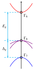
is the “atomic” SO parameter defining the split-off gap; see Fig. 1(a), which schematically shows the conduction and valence bands of a zincblend structure. The circles indicate the eigenenergies.
The Kane model treats exactly the conduction-valence band couplings within the truncated set of eight band-edge wave functions. It is important to emphasize that we have neglected contributions from the -dependent SO term in Eq. (7), when constructing the Kane Hamiltonian (9).Kane (1957) The SO interaction is accounted for only within the zone center Schrödinger’s equation (5) (parameter above). The diagonalization of the Kane Hamiltonian gives the dispersions around the point. It is known that the Kane model presented here is not accurate for valence bands Bastard (1988) (e.g., wrong sign of the heavy hole masses). However, it provides a simplified and accurate description for the conduction electrons, which is the focus of our work. Next we discuss the Kane model in the context of heterostructures.
II.3 Kane model for quantum wells
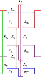
Following Refs. Bastard, 1988 and Winkler, 2003 we can straightforwardly generalize the bulk Kane model of Sec. II.2 to heterostructures. Essentially, we have to introduce position-dependent (growth direction) band gaps which represent the different compounds comprising the heterostructure, e.g., Fig. 1(b). In this case, the form of the resulting Kane Hamiltonian is similar to that of bulk but with -dependent diagonal matrix elements and with . More specifically, defining , , and , we have for the double quantum well of Fig. 1(b)
| (12) | ||||
| (13) | ||||
| (14) |
with , and being the fundamental and split-off band gaps in the well region, respectively, and
| (15) |
where is a dimensionless profile function describing the shape of a square well of width [and unit depth, Fig. 1(b)]; similarly, describes the shape of the central square barrier, Fig. 1(b). The parameters , , , , , and denote the relevant band offsets between the well and the lateral and central barriers for conduction and valence bands. Defining the zero of energy at the bottom of the conduction well [see Fig. 1(b)], we have
| (16) | ||||
| (17) |
The corresponding expressions for a single well can readily be obtained from the above by setting the ’s to zero (i.e., no central barrier).
Finally, note that we have added a “Hartree” potential in the diagonal elements; see Eqs. (12)–(14). The Hartree potential here contains contributions from the electron-electron interaction (mean field) relevant in quantum wells containing many electrons, the external gate potentials, and the modulation-doped potential (i.e., ionized impurities outside the well region). In Appendix A, we describe in detail these distinct contributions to and how they are calculated in our system. As we will see next, both and the structural confining potentials contribute to the effective SO coupling for electrons.
III Effective spin-orbit Hamiltonian for electrons
III.1 Folding down
Since we are interested in SO effects for the conduction electrons, here we derive an effective Hamiltonian for them. To this end, let us rewrite our Hamiltonian [Eq. (9)] in the block form,
| (18) |
where is a diagonal matrix in the sector (conduction band) with identical diagonal elements [(12)] and is a diagonal matrix in the sectors and (valence bands) with diagonal elements [(13)] and [(14)], respectively. The matrix can be read off directly from the corresponding block in Eq. (9).
Using the block form of our Hamiltonian (18)) the eigenvalue problem can be written in the compact form
| (19) |
where is a two-component spinor (conduction sector) and is a six-component spinor (valence sector). Straightforward manipulationsBastard (1988); Winkler (2003) yield the effective Schrödinger’s equation
| (20) |
with
| (21) |
and is a properly renormalized conduction-electron spinor.ren
III.2 Energy denominator expansions
Since and are the largest energy scales in our system, i.e.,
| (26) | ||||
| (27) |
we can expand the energy denominators in the ’s [Eqs. (24) and (25)] in the form
| (28) | ||||
| (29) |
For the diagonal matrix elements we keep only zeroth-order (i.e., energy-independent) terms, while for the off-diagonal matrix elements we keep in addition the first-order terms as they give the lowest non-vanishing contribution (because the off-diagonal matrix elements contain derivatives with respect to ). Straightforwardly, we then obtain the energy-independent one electron Hamiltonian
| (30) |
where
| (31) |
[the subscript “sc” emphasizes that the potential is to be determined self-consistently – see Appendices A and B] andBernardes et al. (2007)
| (32) | ||||
| (33) | ||||
| (34) |
with
| (35) | ||||
| (36) | ||||
| (37) |
III.3 Projection into the quantum well subbands
Here we define a quasi-two-dimensional (2D) model starting from the three-dimensional (3D) Hamiltonian (30). The idea is essentially to obtain a 2D effective model similar to the well-known Rashba model, but now for the case of wells with many subbands. To this end we (i) first project [(30) into the spin-degenerate eigenstates of [Eq. (31)] (note that does not contain the SO interaction):zaw , , , and (or ), which correspond to the subband energies , with being the quantized levels of the well, and then (ii) consider a reduced set of subbands (e.g., two) by truncating the basis set used. In this section we simply assume that we know the eigensolutions of ; later on we actually calculate them within a self-consistent procedure, from which we can explicitly determine the relevant SO coupling constants in our problem.
The matrix elements of in the basis are
| (38) | ||||
| (39) |
with the generalized SO couplings
| (40) |
where
| (41) | ||||
| (42) | ||||
| (43) |
The coefficients , , and denote the contributions from the Hartree potential, the quantum-well edges, and the central barrier edges, respectively. It is convenient to split the Hartree contribution into two terms, i.e., , where is the purely electronic Hartree potential and denotes the contributions from the external gate potential and the modulation doping potential. Hence . This separation will be useful when discussing our results.
We emphasize that the diagonal (in ) parameters correspond to the Rashba coupling in the th subband, i.e., . The off-diagonal terms arise due to the intersubband coupling. Interestingly, these new SO terms can be non-zero even in structurally symmetric wells, since they arise from quantum-well states of distinctive parities.
For completeness we present here the linearized Dresselhaus couplingsire in the th subband
| (44) |
where the constant is the bulk Dresselhaus SO parameter. Jancu et al. (2005) We can easily rewrite the above expression in the more convenient form
| (45) |
In Sec. V we shall use the above form to discuss how the Dresselhaus couplings vary as a function of the system parameters.
III.4 Two-subband case
To illustrate the procedure of Sec. III.3, let us explicitly work out here the case of a quantum well with only two subbands . In Sec. V we shall investigate in detail the SO couplings for single and double quantum wells with two subbands.
III.4.1 4x4 Hamiltonian
III.4.2 Eigensolutions
The energy eigenvalues of Eq. (46) are straightforward to obtain:
| (48) |
where are spin quantum numbers and are the subband (or pseudo spin) indices, and
| (49) |
The corresponding (normalized) eigenvectors are
| (50) |
where
| (51) |
III.4.3 SO-induced effective mass renormalization
Expanding the energy dispersions [Eq. (48)] around , we obtain to second order
| (52) |
where are the effective masses
| (53) |
where and . Note that the mass renormalization is solely due to the intersubband-induced SO coupling . For the realistic wells we investigate here for single wells but can reach for double wells (Secs. IV and V).
III.4.4 Determining the SO couplings
As mentioned previously, we determine the SO orbit couplings (here specifically , , and ) from the self-consistent eigensolutions of the quantum well without spin orbit,zaw via Eqs. (40))-(43)). In Sec. IV we detail the quantum well systems investigated and briefly outline the self-consistent procedure used to obtain the eigensolutions (a full description is provided in Appendices A and B). We then present results for single and double wells with two subbands; i.e., we calculate , , and and discuss in detail the several distinct contributions to each of these quantities.
IV Quantum-well systems and self-consistency
Figure 2 shows a schematic view of the quantum-well system we study: a well of width centered at (: growth direction), and two adjacent symmetrically doped regions of widths in the barriers. We also consider double wells by inserting an additional (central) barrier of width in the well region. The doping densities of the left and right regions, and , respectively, can be used to control the degree of structural inversion asymmetry of the wells (in Sec. V, however, we present results only for ). The external gates and , located at the end points , can also be used to control the degree of inversion asymmetry and to vary the areal electron density in the well.
Since our wells have many electrons and are subject to external gates, we have to solve the Schrödinger and Poisson equations self-consistently (“Hartree approximation”Enderlein and Horing (1999)) in order to determine their potential profile [see Eq. (33)] and corresponding eigenfunctions and eigenenergies. In Appendices A and B we describe in detail our standard self-consistent procedure.

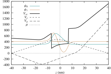
Before going into the discussion of the SO couplings in detail, let us first have a look at the outcome of a typical self-consistent simulation we perform. Figure 3(a) shows the self-consistent potential (thick solid line) for a single well with two subbands; the corresponding self-consistent wave functions and are also shown. The energies of the two lowest subband edges (see levels in the well) are meV and meV ( meV). Here we fix the chemical potential at meV with respect to the origin (“constant chemical potential model”, see below) and set the external gates to and meV. The two subbands are occupied with areal densities cm2 and cm2, respectively. The electronic Hartree potential (short dashed line) and the the external gates (plus modulation doping) contribution (long dashed line) are also shown. Figure 3(b) shows the corresponding “force fields” arising from the confined electrons in the well and coming from the doping regions ( nm to nm) plus the external gates ( and will be useful when discussing the SO couplings further below). Using the self-consistent solutions , , we can straightforwardly calculate the relevant SO couplings [via Eqs. (40)–(43)]: meV nm, meV nm, meV nm, meV nm, and meV nm.

V Results
Here we focus on single and double quantum wells with only two subbands. More specifically, we calculate three SO couplings: the intersubband-induced SO coupling and the two Rashba-type couplings and . We consider two experimentally relevant cases: the constant areal density (-constant) and the constant chemical potential (-constant) models. In our simulations we always keep as a reference potential and vary ; see Fig. 2. For completeness, we also calculate the two Dresselhaus constants and [see Eq. (44)] within each subband.
V.1 Single wells
| = | = | = | = | ||||||||
| = | = | = | = | ||||||||
| = | = | = | = | ||||||||
| = | = | = | = | ||||||||
| = | = | = | = |
V.1.1 Single-well parameters
We consider a realistic Al0.48In0.52As/Ga0.47In0.53As single quantum well.Koga et al. (2002, 2006) We assume doping densities cm-3 with widths nm (“sample 3” in Ref. Koga et al., 2002). Table 2 summarizes band parameters, potential offsets,Vurgaftman et al. (2001) well widths, and other important parameters of our system. The coefficients and in Tab. 2 are defined in Eq. (36) and Eq. (35), respectively. Here, the Dresselhaus parameter in Eq. (44) is assumed to be the same as that of the GaAs (see Ref. Jancu et al., 2005).
V.1.2 SO couplings: single wells
Figure 4 shows the strength of the Rashba (, ; dashed lines), Dresselhaus (, ; dotted lines) and intersubband-induced (, solid line) SO couplings as functions of the gate voltage , for both the -constant and the -constant models, Figs. 4(a) and 4(b), respectively. At eV, our sample is completely symmetric and, as expected, the Rashba couplings and are zero. We note that the Dresselhaus couplings and are practically constant in both models. This follows from Eq. (45) which shows that in each subband the Dresselhaus coupling is essentially the difference between the expected value of the self-consistent potential in the respective subband and the corresponding eigenenergy. The Rashba couplings, on the other hand, vary considerably with , although showing a similar trend in both models. Interestingly, they change signs about (symmetric configuration), but always with . Our calculated within the -constant model [Fig. 4(b)] is consistent with the measurements of this quantity by Koga et al.,Koga et al. (2002, 2006) whose samples have a constant chemical potential.
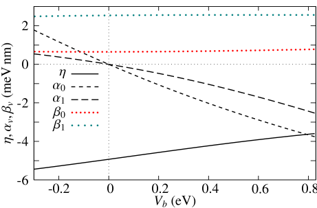
The new intersubband-induced coupling [see the solid lines in Figs. 4(a) and 4(b)] is non-zero even in the symmetric well configuration (). It has a strength comparable to the Rashba and is at least twice as large as the Dresselhaus. In contrast to the Rashba couplings, the intersubband SO does not change sign with . In fact, for the single well investigated here is almost constant with , although it varies slightly more in the -constant model [compare the solid curves in Figs. 4(a) and 4(b)].
To more easily understand the results above, we analyze the several contributions to the SO couplings separately. To this end, we rewrite [see comments following Eq. (40)] for a single well in the form
| (54) |
where we have set in (40), i.e., no central barrier contribution, and have split the Hartree contribution into its purely electronic and the external gate (plus doping potential) parts. Hence, for two subbands, each of the SO couplings has three contributions: , and . Figures 5(a)–5(c) show the above contributions separately for the -constant case (similar results hold for the -constant model, in the parameter range studied).
Figure 5(a) shows that the external gates and doping contributions to ( curve) are essentially zero, while the electronic Hartree contribution ( curve) and the structural ( curve) contributions are comparable in magnitudes and both negative. In contrast, for both and the largest contributions come from the external gates together with doping regions [see the curve in Fig. 5(b) and the curve in Fig. 5(c)]; these account for 60% of and 100% of . The electronic Hartree contribution is negligible in [curve in Fig. 5(c)] while the structural part () accounts for about 30% of it. On the other hand, the structural and electronic Hartree contributions in essentially cancel out (same magnitude and opposite signs); cf. the and curves in Fig. 5(c).


We can understand the above remarks by looking at the self-consistent potentials and the “force fields” (short dashed curve) and (long dashed curve) – note that , , – in Fig. 3(b). This figure was obtained for eV, but it does display the general behavior for all quantities shown. The force field is essentially constant, except within the donor regions where the wave functions are vanishingly small. Hence, the matrix element [see Eqs. (40)–(43)] is approximately linear in the external gate . This explains why the Rashba couplings are strongly modulated by external gates. This is even more so for , Fig. 5(c), for which the structural and electronic contributions cancel out. Looking at the wave functions and and the force field in Fig. 3(b), we can see that the electronic Hartree contribution () is almost zero (though slightly negative) for the lowest subband and positive for the first subband. The structural well contributions [see Eq. (42)] to are similar for both subbands, though , because the nonzero biases () cause the wave functions to shift toward one side of the well [e.g., eV in Fig. 3(a)].
On the other hand, the contribution to the intersubband coupling is essentially zero since the wave functions [ and in Fig. 3(a)] are orthogonal and, again, is constant. Hence is not as sensitive to the external gates as the Rashba couplings. Most of the modulation of arises from the electronic Hartree and structural contributions, which both have the same sign and magnitude as shown in Fig. 5(a).
V.2 Double well
V.2.1 Double-well parameters
Table 3 shows the band parametersVurgaftman et al. (2001); Jancu et al. (2005) for the double quantum well Al0.4In0.6Sb/InSb with one central barrier InSb/Al0.12In0.88Sb. Hereafter we refer to this heterostructure as InSb double well. The meaning of some of these parameters (e.g., band offsets) can be seen in Figs. 1 and 2.
| = | = | = | = | ||||||||
| = | = | = | = | ||||||||
| = | = | = | = | ||||||||
| = | = | = | = | ||||||||
| = | = | = | = |
V.2.2 SO couplings: double-well case
Figure 6 shows the Rashba , Dresselhaus , and intersubband-induced SO couplings as functions of the gate voltage (here again ) for both the -constant (a) and -constant (b) models. We first discuss the -constant model [Fig. 6(a)]. Here the Rashba couplings (dashed lines) are most sensitive to the external bias , being essentially the largest of all SO couplings for very asymmetric structures (i.e., high biases). The Dresselhaus couplings (dotted lines) are almost identical
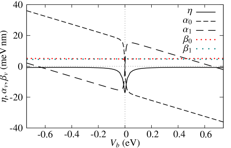
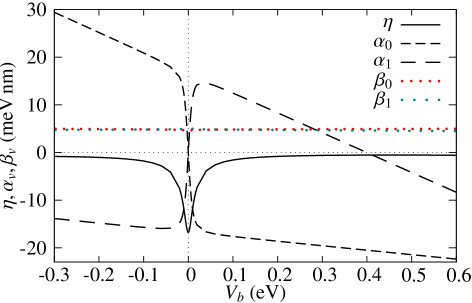
() and mostly independent of the external gates. The SO coupling (solid line) is an even function of the external gate and presents a “resonant behavior” around the eV configuration, at which our sample is symmetric. While the Rashba couplings are both zero at this symmetric configuration, we note that they are odd functions of the external gate (with ), have opposite signs and abruptly change magnitudes around (over a 40 meV wide region). For the -constant model [Fig. 6(b)], a similar picture as above also holds; note, however, that in contrast to the -constant model, in the -constant case the positive and negative bias configurations are not equivalent as they correspond to the well having different numbers of electrons.
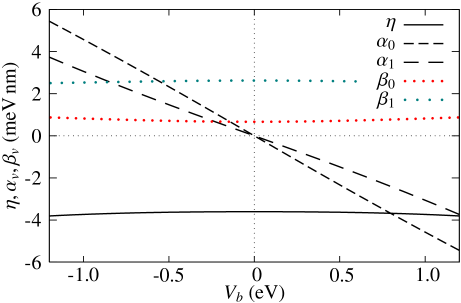
For completeness we show in Fig. 7 the behavior of all coupling constants near the symmetric point eV for the double well in Fig. 6(a). Note that the Dresselhaus couplings and present a (double) crossing over a 160 meV wide region [see Fig. 7(b)]. However, this is a minor effect: note the change in the scale of the vertical axis. While the resonant behavior of is accompanied by an enhancement of about 10 in its magnitude [see Fig. 6(a)], we see no substantial change in the magnitudes of the ’s near the zero-bias case [cf. Figs. 7(a) and 7(b)].


The relative strengths of the Rashba and Dresselhaus coupling constants to the intersubband-induced SO coupling are shown in Fig. 8. The Rashba couplings have the largest strengths (note the pre-factors in front of in the legends). In contrast to , the linear behavior of the Rashba ratios near (see insets) shows that and undergo similar variations near the symmetric configuration. As observed before, the intersubband-induced coupling becomes important near (Fig. 6).
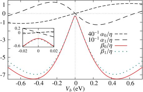
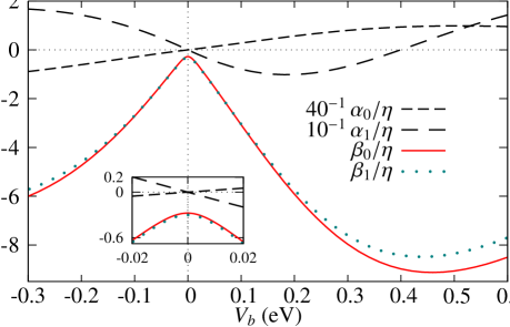
Figure 9 (similar to Fig. 5 for the single-well case) shows the several contributions to each of the SO couplings , and for the double-well case. Here, in addition to the electronic Hartree, the gate (+ doping regions), and the well contributions, there is an additional structural term arising from the central barrier (superscript b). A general feature in Figs. 9(a)–9(c) is that the structural


contributions (well and central barrier) almost cancel out because they have opposite signs (see the curves with superscripts w and b). These terms have opposite signs because the derivatives (well) and (barrier), which enter the coupling constants [see Eqs. (40), (42), and (43)], have opposite slopes. Similarly to the single-well case [Fig. 5(a)] the contribution of the external gates (which includes the doping regions) to the intersubband SO coupling is vanishingly small [see the curve in Fig. 9(a)]. Hence, is mostly due to the electronic Hartree contribution [curve in Fig. 9(a)]. In addition, the gate contribution to and for the InSb double well is linear in as for the single-well case. Hence, the Rashba couplings and for the double InSb well are essentially determined by the electronic (Hartree) contribution and are modulated by the gate contribution. Summarizing: looking at Fig. 9, we can see that (i) the structural contributions (well and barrier; dashed curves) almost cancel out, and (ii) the external gate (dotted curves) modulates the Rashba couplings ; therefore, for the double well investigated here (iii) most of the strength of these three coupling constants (, , and ) comes from the electronic contribution (dot-dashed curves).
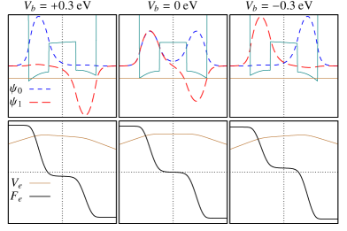
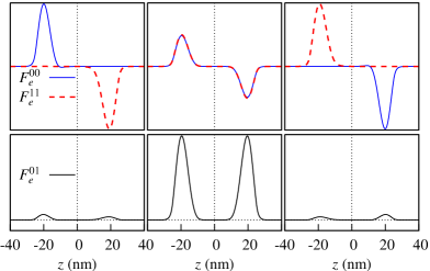
It is instructive to investigate in more detail how the resonant behavior in comes about, as well as the abrupt changes in the Rashba couplings; see Fig. 6. This can be accomplished by looking more closely at the self-consistent wave functions of the InSb double well around the symmetric configuration (). The top row in Fig. 10 shows the self-consistent potential profile of the double well and the normalized wave functions (short dashed line) and (long dashed line) for the lowest and for the first excited subbands at three distinct gate voltages: eV, eV and eV (left, center, and right columns, respectively). For positive bias is mostly localized in the left well and in the right well, while for negative biases this configuration is reversed. The electronic Hartree contribution to the potential energy and the corresponding force field are shown on the second row, thin and thick lines respectively. Notice that is practically zero in the central barrier region ( nm) and has opposite signs within the wells ( nm and nm). Hence the quantities , and have the forms shown on the third and fourth rows. The integral over of these quantities defines the electronic Hartree contributions to the spin-orbit couplings , , and , i.e., , , and , respectively. Since the electronic Hartree contributions dominate over the others, see Figs. 9(a)–9(c), the abrupt changes in the Rashba couplings and the resonant behavior of around follow straightforwardly.
V.2.3 Density anticrossings and effective masses
Figures 11(a) and 11(b) show anti-crossings of the areal densities for the InSb double well near the symmetric configuration Fletcher et al. (2005), where the strength of the intersubband-induced SO coupling is the strongest ( meV nm) while the the energy difference between the subband edges ( meV) is the smallest. In accord with Eq. (52), we find an appreciable change in the bulk effective mass near sar . The ratio [see Eq. (53)] is shown in Fig. 11(c) and the ratio in Fig. 11(d). These intersubband-SO-induced changes in the effective masses may have a sizable effect on the measured mobilities and cyclotron frequencies in InSb wells.

VI Summary
Starting from the Kane model in heterostructures, we have derived in some detail an effective electron Hamiltonian which contains a new intersubband-induced SO interaction term which arises in quantum wells with more than one quantized subband. Unlike the usual Rashba SO term, the intersubband SO coupling here is non-zero even for symmetric wells. For structurally asymmetric wells we have also accounted for the Rashba-type SO interaction within each subband.
We have also outlined the projection procedure (“folding down”) to obtain quasi-2D Hamiltonians by integrating out the confined variables. For two subbands in asymmetric wells we find a quasi-2D Hamiltonian resembling Rashba’s, but containing three SO couplings: the two Rashba couplings and and the intersubband SO coupling . For this two-subband case, we have investigated thoroughly these three SO couplings for realistic modulation-doped single and double wells. By performing a detailed self-consistent calculation in which we solve both Poisson’s and Schrödinger’s equation iteratively, we have determined the strengths of , , and .
Each of these coupling strengths contains contributions arising from (i) the potential-well (and barrier) offsets, (ii) the electronic Hartree potential, and (iii) the external gate potential plus the modulation doping potential. We have performed our simulations by either keeping the areal electron density in the well fixed (-constant model) or by keeping the chemical potential fixed (-constant model). In the parameter range investigated, both models give similar result for the calculated SO couplings.
For the single well investigated, is mostly determined by the external gate (+ modulation doping) contribution; with the structural + electronic Hartree being about half of that of the gate. On the other hand, is essentially determined by the external gate (+ modulation doping) contribution, since the electronic Hartree and the structural contributions cancel out. The intersubband SO coupling is essentially determined by the electronic Hartree potential and the structural potential contributions (both of the same order); the external gate (+ modulation doping) potential contribution to is nearly zero. Hence, while and can be modulated by the external gate potential, is only slightly influenced by it.
For double wells the SO couplings show more peculiar behaviors. While the Rashba couplings and abruptly change magnitudes and signs around the symmetric configuration (zero external bias), the intersubband-induced SO coupling presents a resonant behavior being enhanced by a factor of 10 (with no sign change) around this point. For the double well investigated the structural contributions to , and , due to the potential offsets of the edges of the well and the central barrier, cancel out. In addition, the contribution of the external gate (+ doping region) to is vanishingly small (as for the single-well case). Interestingly, the dominant contribution to all three SO couplings , , and comes from the electronic Hartree potential. However, this contribution is highly influenced by the external gate, particularly around the symmetric configuration as the electrons can easily localize in either well for slight (positive or negative) changes in the gate.
Finally, we have also calculated the effective mass renormalization due to the intersubband SO interaction (the Rashba-type interaction does not produce a mass change). For the double well investigated, we find that this mass renormalization is the largest () around the symmetric potential configuration (zero external bias), for which the splitting of the two subbands is the smallest. This mass change can possibly have an effect on mobility and cyclotron-resonance measurements.
Acknowledgements.
We thank G. J. Ferreira, H. J. P. Freire, and L. Viveiros for useful discussions. This work was supported by the Swiss NSF, the NCCR Nanoscience, JST ICORP, CNPq and FAPESP.Appendix A Self-consistent procedure
A.1 Effective Schrödinger equation
The single-particle electron Hamiltonian of our quantum wells [Eq. (31))] is clearly separable. The transverse motion (x,y) is free while that along the z direction is confined by the quantum well. To solve the corresponding Schrödinger equation we assume a wave function of the form
| (55) |
( is a normalizing area) which leads to the 1D Schrödinger equation
| (56) |
from which we obtain the quantized energy levels and wave functions . As we shall see, the subband structure of the well and the corresponding total wave function will be used (within a self-consistent procedure) to construct the electron charge density, from which the corresponding Hartree potential can be obtained via the Poisson equation.
As mentioned in Sec. III.2 in Eq. (56) contains not only the structural confining potential but also the “Hartree contributions” (i) the purely electronic mean-field potential (electronic Hartree potential) and (ii) the external gate potential plus the modulation doping potential. Further down we discuss these contributions in detail. Each of these contributions is determined from a Poisson equation with an appropriate charge distribution and boundary condition.
A.1.1 Self-consistency
Since the electronic charge distribution () depends on the detailed form of the several potentials (modulation doping, gates, and electronic Hartree), and these, in turn, depend on , we have to solve the problem self-consistently. The standard procedure is as follows: (i) to solve Eq. (56)) with an initial guess for which we take to be just the structural potential plus the external gates and modulation doping potential [i.e., in the first run we do not include the electronic Hartree potential ]; (ii) to construct the electronic charge density [from the eigenfunctions obtained in step (i)] and the corresponding via Poisson equation; and (iii) to solve again the Schrödinger equation with the new , which in this new iteration includes (as well as the other potentials: gates, modulation doping, and structural confinement). We repeat this process until convergence is attained.
A.1.2 Numerics
We use the sixth-order Numerov method to solve the Schrödinger equation.Numerov (1924); Blatt (1967); Chow (1972); Agarwal and Wang (2001) Poisson equation (see Sec. A.2) is solved via a semi-analytical Numerov method.Bernardes (2007) All numerical integrations are performed using a Gaussian integration method.Slater (1964) In our numerical implementation we use the dimensionless form of Eq. (56),
| (57) |
where
| (58) |
We choose nm as our length unit and as the relevant energy scale.
A.2 Poisson equations for the electronic and gate plus modulation doping potentials
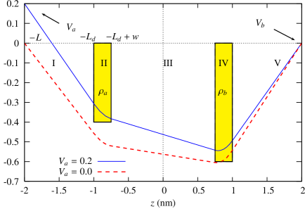
The self-consistent electronic potential energy can be split in two parts, . described the structural quantum-well potential. The “Hartree” contribution arises from the electronic charge density and from the external gates plus the modulation doping regions (symmetrically located around the well; see Fig. 12). Figure 12 also shows the Dirichlet boundary conditions and , which are in fact the external gates at the end points of our system.
A.2.1 Gate+modulation doping potential
We can write separate Poisson equations for and as these arise from distinct charge densities. For we have (see Fig. 12)
| (59) |
where is the permittivity, is the dielectric constantSamara (1983); Lide (2004) and are the doping densities. From the continuity of and its first derivative and assuming the Dirichlet boundary conditions and , we find
| (60) |
with
| (61) |
where the constants are given in Appendix B. Figure 12 shows two solutions of Eq. (59), both having and (dashed line) and .
A.2.2 Electronic Hartree potential
The electronic Hartree contribution is determined from
| (62) |
with (including spin)
| (63) |
where
| (64) |
and
| (65) |
We solve Eq. (62) for using an accurate Numerov scheme Bernardes (2007) with the Dirichlet boundary conditions . Similarly to the Schrödinger equation in Eq. (57)), we find it convenient here to write the Poisson equation (62) in a dimensionless form
| (66) |
where is the energy scale given in Eq. (58) and
| (67) |
A.2.3 Electron density and chemical potential
From the total electronic charge
| (68) |
we can straightforwardly [using Eq. (63))] obtain the total areal concentration of electrons
| (69) |
with the ’s denoting the subband occupations
| (70) |
When is fixed (i.e., the -constant model), we can determine the chemical potential from Eq. (69),
| (71) |
Appendix B Coefficients ’s
Using the continuity of and its first derivative together with the (Dirichlet) boundary conditions at the end points and , we can determine the coefficients ’s appearing in Eq. (60). In the regions I and V we find
| (72) | ||||
| (73) | ||||
| (74) | ||||
| (75) |
with
| (76) |
and and defined in Eq. (61). In the modulation doping regions II and IV, we have
| (77) | ||||
| (78) | ||||
| (79) | ||||
| (80) |
In the central region III, we have
| (81) | ||||
| (82) |
References
- Datta and Das (1990) S. Datta and B. Das, Appl. Phys. Lett. 56, 665 (1990), see also J. C. Egues, G. Burkard, and D. Loss, ibid. 82, 2658 (2003), for a spin FET proposal with additional spin control due to spin-orbit induced interband coupling.
- Rashba (1960) E. I. Rashba, Sov. Phys. Solid State 2, 1109 (1960).
- Bychkov and Rashba (1984a) Y. A. Bychkov and E. I. Rashba, J. Phys. C 17, 6039 (1984a).
- Bychkov and Rashba (1984b) Y. A. Bychkov and E. I. Rashba, JETP Lett. 39, 78 (1984b).
- Engels et al. (1997) G. Engels, J. Lange, T. Schäpers, and H. Lüth, Phys. Rev. B 55, R1958 (1997).
- Akazaki et al. (1997) J. N. T. Akazaki, H. Takayanagi, and T. Enoki, Phys. Rev. Lett. 78, 1335 (1997).
- Dresselhaus (1955) G. Dresselhaus, Phys. Rev. 100, 580 (1955).
- Wolf et al. (2001) S. A. Wolf, D. D. Awschalom, R. A. Buhrman, J. M. Daughton, S. von Molnár, M. L. Roukes, A. Y. Chtchelkanova, and D. M. Treger, Science 294, 1488 (2001).
- Awschalom et al. (2002) D. Awschalom, D. Loss, and N. Samarth, eds., Semiconductor Spintronics and Quantum Computation (Springer, New York, 2002).
- Žutić et al. (2004) I. Žutić, J. Fabian, and S. D. Sarma, Rev. Mod. Phys. 76, 323 (2004).
- Schliemann et al. (2005) J. Schliemann, D. Loss, and R. M. Westervelt, Phys. Rev. Lett. 94, 206801 (2005).
- Schliemann et al. (2006) J. Schliemann, D. Loss, and R. M. Westervelt, Phys. Rev. B 73, 085323 (2006).
- Schliemann et al. (2003) J. Schliemann, J. C. Egues, and D. Loss, Phys. Rev. Lett. 90, 046801 (2003).
- Bernevig et al. (2006) B. A. Bernevig, J. Orenstein, and S. C. Zhang, Phys. Rev. Lett. 97, 236601 (2006).
- Bernardes et al. (2007) E. Bernardes, J. Schliemann, M. Lee, J. C. Egues, and D. Loss, Phys. Rev. Lett. 99, 076603 (2007).
- Krich and Halperin (2007) J. J. Krich and B. I. Halperin, Phys. Rev. Lett. 98, 226802 (2007).
- Bernardes et al. (2006) E. Bernardes, J. Schliemann, J. C. Egues, and D. Loss, Phys. Stat. Sol. (C) 3, 4330 (2006).
- Kane (1957) E. O. Kane, J. Phys. Chem. Solids 1, 249 (1957).
- Bastard (1988) G. Bastard, Wave Mechanics Applied to Semiconductor Heterostructures (Halsted, Les Ulis Cedex, France, 1988).
- Winkler (2003) R. Winkler, Spin-Orbit Coupling Effects in Two-Dimensional Electron and Hole Systems, no. 191 in Springer Tracts in Modern Physics (Springer, New York, 2003).
- Jancu et al. (2005) J.-M. Jancu, R. Scholz, E. A. de Andrada e Silva, and G. C. L. Rocca, Phys. Rev. B 72, 193201 (2005).
- Wood and Zunger (1996) D. M. Wood and A. Zunger, Phys. Rev. B 53, 7949 (1996).
- Ivchenko and Pikus (1997) E. L. Ivchenko and G. E. Pikus, Superlattices and Other Heterostructures, no. 110 in Springer Series in Solid-State Sciences (Springer, New York, 1997).
- Darnhofer and Rössler (1993) T. Darnhofer and U. Rössler, Phys. Rev. B 47, 16020 (1993).
- Vurgaftman et al. (2001) I. Vurgaftman, J. R. Meyer, and L. R. Ram-Mohan, J. Appl. Phys. 89, 5815 (2001).
- (26) The renormalization of the conduction wave function is crucial to obtain an effective Pauli-like equation which properly includes the Darwin term and other higher other corrections. Winkler discusses this point in detail in Ref. Winkler, 2003 (chapters 5 and 6).
- (27) Here we neglect the Darwin and all higher-order terms and focus on only the Rashba-like contributions.
- (28) The Kane effective mass in Eq. (32) neglects corrections from higher bands; here we use as a parameter determined from experiment.
- (29) Here we are following a procedure similar to that used by W. Zawadzki and P. Pfeffer, Semicond. Sci. Technol. 19 R1 (2004), that is, we neglect the spin-dependent boundary conditions along the growth direction. These authors have also performed a detailed analysis considering the effects of the spin-dependent boundary conditions (along the growth axis of the well) on the SO energy splittings. They found that the inclusion of the spin-dependent boundary conditions gives rise to small corrections to the calculated SO energy splittings, with more sizable corrections for heavily-doped ( cm-2) narrower band gap heterostructures (e.g. InAs/In0.8Al0.2As). However, the influence of the spin-dependent boundary conditions on the Rashba couplings () is not mentioned in their study. We believe that the inclusion of the spin-dependent boundary conditions (along the growth) in our problem will not alter the results in any essential way (certainly not qualitatively); For an alternate description of the Rashba effect using a multi-band approach see U. Ekenberg and D. M. Gvozdic, arXiv:0801.0089v1. As these authors emphasize, the contrasts between these two descriptions deserve further study.
- (30) For a model which accounts for the Rashba and Dresselhaus terms on the same footing, see, e.g. F. V. Kyrychenko, C. A. Ullrich and I. D’Amico, J. Mag. Magn. Mat. (to be published); authors investigate whether the intersubband SO coupling discussed here should be accounted for when extracting the spin Coulomb drag from intersubband spin plasmon linewidths; they conclude it has a negligible effect on that property.
- (31) R. J. Warburton, C. Gauer, A. Wixforth, J. P. Kotthaus, B. Brar and H. Kroemer, Phys. Rev. B 53, 7903 (1996); E. L. Ivchenko and S. A. Tarasenko, JETP 99, 379 (2004); J. B. Khurgin, Appl. Phys. Lett. 88, 123511 (2006), have investigated optical intersubband couplings (dipolar approximation) in quantum wells. Even though these authors have taken into account the spin-orbit interaction (via the approximation) when calculating these light-induced transitions, we emphasize that the intersubband coupling we consider in our work [Eqs. (34)–(37) or (40)–(43)] is of a different nature. By looking at, e.g., the intersubband matrix element in Eqs. (15)–(17) in the work of Ivchenko and Tarasenko, we can see that their matrix element (i) is proportional to the amplitude of the electromagnetic vector potential and, more importantly, that (ii) it is independent of the Kane matrix element . Our intersubband coupling, on the other hand, is directly proportional to the Kane matrix element [defined in our Eq. (10)] and does not depend on a vector potential (we do not treat optical absorption, i.e., in our work). We believe, however, that intersubband light absorption may provide an interesting means to experimentally probe and contrast the spin orbit interactions (in the single and double wells) investigated here. This issue will be addressed in a future work.
- Enderlein and Horing (1999) R. Enderlein and N. J. Horing, Fundamentals of Semiconductor Physics and Devices (World Scientific, Singapore, 1999).
- Koga et al. (2002) T. Koga, J. Nitta, T. Akasaki, and H. Takayanagi, Phys. Rev. Letts. 89, 046801 (2002).
- Koga et al. (2006) T. Koga, Y. Sekine, and J. Nitta, Phys. Rev. B. 74, 041302 (2006).
- Fletcher et al. (2005) R. Fletcher, M. Tsaousidou, T. Smith, P. T. Coleridge, Z. R. Wasilewski, and Y. Feng, Phys. Rev. B 71, 155310 (2005).
- (36) For a detailed calculation of the Rashba SO-induced changes of the quasi-particle effective mass in a two-dimensional Fermi Liquid, see D. S. Saraga and D. Loss, Phys. Rev. B 72, 195319 (2005).
- Numerov (1924) B. V. Numerov, Mon. Not. R. Astron. Soc. 84, 592 (1924).
- Blatt (1967) J. M. Blatt, J. Comp. Phys. 1, 382 (1967).
- Chow (1972) P. C. Chow, Am. J. Phys 40, 730 (1972).
- Agarwal and Wang (2001) R. P. Agarwal and Y. M. Wang, Comp. Math. App. 42, 561 (2001).
- Bernardes (2007) E. Bernardes, arXiv0712.1706v1 (2007).
- Slater (1964) L. J. Slater, in Handbook of Mathematical Functions, edited by M. Abramowitz and I. A. Stegun (Dover, New York, 1964), p. 503.
- Samara (1983) G. A. Samara, Phys. Rev. B 27, 3494 (1983).
- Lide (2004) D. R. Lide, ed., Handbook of Chemistry and Physics (CRC, Boca Raton, 2004).