Vortex states in patterned exchange biased NiO/Ni samples
Abstract
We investigated the magnetization reversal of arrays of exchange biased NiO/Ni squares with superconducting quantum interference device magnetometry and micromagnetic simulations. The edges of the squares were 0.5, 1.5, and 3.0 m long. The NiO/Ni structures exhibit vortexlike hysteresis loops and micromagnetic calculations show that this feature is due to several vortices nucleating in the islands. Furthermore, for the arrays with squares of 1.5 m edge length, the sign of the exchange bias field changes, as compared to the same continuous NiO/Ni layer. We attribute the vortex nucleation and the change of the exchange bias field to the interplay between shape and unidirectional anisotropy.
pacs:
75.70.Kw, 75.30.Gw, 75.60.Jk, 75.75+aI INTRODUCTION
One of the most renowned features of the exchange bias (EB) effect, which results from the exchange coupling between ferromagnetic (F) and antiferromagnetic (AF) layers, is a shift of the hysteresis loop away from zero field. It is associated with a frozen-in unidirectional anisotropy, induced, e.g. by cooling of the EB system through the Néel temperature in an applied magnetic field. Due to the intriguing properties underlying the EB phenomenon and its relevance for magnetic recording applications it is under persistent study since the seminal paper by Meiklejohn and Bean in 1956 Meiklejohn and Bean (1956) (for recent reviews see Refs. Nogués and Schuller (1999); Kiwi (2001); Stamps (2000); Berkowitz and Takano (1999); Radu and Zabel (2008)). Especially the characteristics of EB in micro- to submicrometer dots are of considerable interest with regard to the miniaturization of industrially manufactured spin valves. Moreover, from a fundamental viewpoint, it is of high importance to probe the effects of confinement on the EB effect. Technical improvements in the fabrication of nano- and microstructures in the past years have made a closer study of EB in micro- to submicrometer dots possible Nogués et al. (2005).
In exchange biased nanostructures in addition to the unidirectional anisotropy and the intrinsic magnetocrystalline anisotropy of the AF and F layers, the shape anisotropy is also significant. The interplay between these anisotropies is crucial for domain formation and remagnetization processes in nanostructures Eisenmenger et al. (2005); Popova et al. (2005); Li et al. (2005). While vortex formation sometimes is observed in the F layer of exchange biased nanostructures Sort et al. (2005), the unidirectional anisotropy may also lead to a collapse of the vortex state that occurs in the same F nanostructure without being in contact to an antiferromagnet Kato et al. (2002). An obvious question is whether the opposite is also possible: vortex formation in the EB system, but no vortex nucleation in the corresponding unbiased F island.
In this paper, we investigate NiO/Ni EB systems. We analyze the magnetic behavior of a continuous NiO/Ni bilayer film and of NiO/Ni square islands of different sizes, both with (EB case) and without (non-EB case) the existence of unidirectional anisotropy. For the patterned samples, we see vortexlike hysteresis loops in the EB case, whereas in the non-EB case several features of a vortex hysteresis loop are missing. Micromagnetic simulations show that the EB field can cause a vortexlike state that is not observed for the same F microstructure.
II EXPERIMENTAL DETAILS
The NiO/Ni samples were fabricated by UHV ion beam sputter deposition and subsequent plasma oxidation. After heating the MgO(001) substrate to 800 ∘C for cleaning its surface, Ni was deposited at a substrate temperature of 100 ∘C with a sputter rate of 0.03 nm/s. The sample was then annealed at 300 ∘C for several hours promoting Ni(001) growth. For a similar sample, Lukaszew et al. Lukaszew et al. (2005) report on an interdiffusion process of the oxygen from the MgO substrate to the Ni, thus creating NiO. While they found evidence of a NiO/Ni EB system, our superconducting quantum interference device (SQUID) measurements of the as-prepared samples never showed an EB effect.
To generate the NiO layer, we used rf plasma oxidation. Test experiments with other oxidation methods showed that plasma oxidation appears to be the only method to obtain exchange biased films by means of oxidizing a Ni layer, probably because a minimum film thickness of the AF layer is required for nonzero EB fields. The plasma oxidation was performed at 200 ∘C with an rf power of 15 W in a separate oxidation chamber, filled with pure oxygen gas at a pressure of mbar.
As explored by small angle x-ray reflectivity and wide angle x-ray diffraction, the resulting Ni layer has a thickness of 4.8 nm and shows a (001) out-of-plane texture. The NiO thickness amounts to 2.0 nm with a (111) out-of-plane texture.
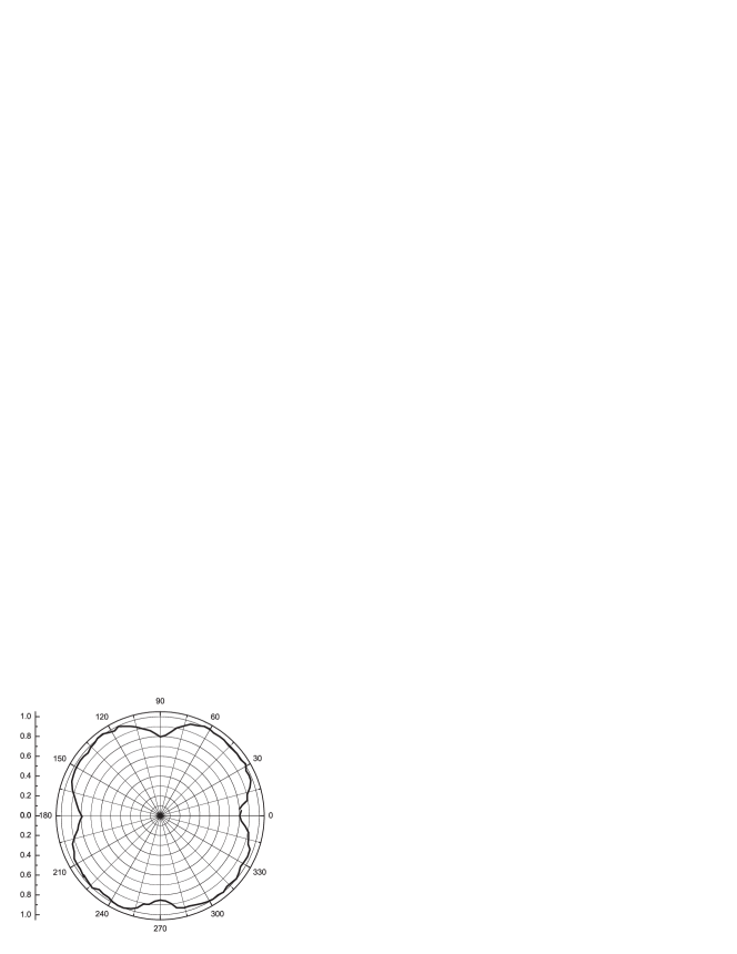
We determined the magnetocrystalline anisotropy of the Ni film with a standard longitudinal magneto-optical Kerr effect (MOKE) setup Schmitte et al. (2002) and observed a four-fold anisotropy, as shown in Fig. 1. The figure displays the value of the remanence normalized to the saturation value as a function of the relative sample rotation angle. The sample was rotated in steps of 5∘. The easy axis lies parallel to the in-plane [1 1 0] direction, in agreement with reports in the literature Hwang et al. (2002).
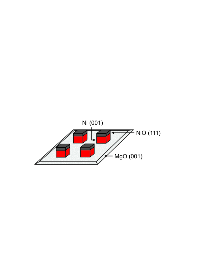
On the same bilayer, square microstructures with different diameters were defined by electron beam lithography. The edges of the squares were aligned along the magnetic easy axis of the continuous Ni film, ,i.e., the [1 1 0] direction. Electron beam lithography was performed with negative photoresist and a FEI Quanta 200 field emission gun (FEG) scanning electron microscope controlled by the Raith ELPHY QUANTUM 4.0 software. After the lithography step, the excess F and AF layers were removed by ion beam etching. The remaining squares had edge lengths of 0.5 m, 1.5 m, and 3.0 m.
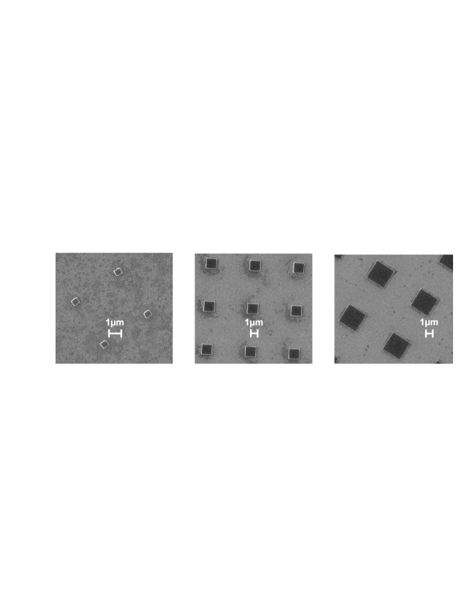
A sketch of the laterally patterned films is shown in Fig. 2. While the diagram displays just four dots, on the sample approximately squares were arranged in order to have a magnetic signal detectable by a SQUID magnetometer. Representative scanning electron microscope (SEM) images of the patterns are shown in Fig. 3.
Subsequently, SQUID magnetometry was used to characterize the EB properties of the continuous bilayer and the patterned films. We employed a rf-SQUID magnetometer by Quantum Design in the reciprocating sample option mode, which is more suitable for weak magnetic signals than the dc stepped-scan technique.
III EXPERIMENTAL RESULTS
For NiO films with a thickness of a few nanometers the Néel temperature is expected to be considerably reduced as compared to the bulk value of 523 K Roth (1958). Alders et al. report a decrease to 295 K for 5 monolayers of NiO(001) (2.1 nm) Alders et al. (1998). For our NiO/Ni samples we proved that the blocking temperature is below 400 K, which makes them suitable for performing the field-cooling procedure in the SQUID magnetometer that provides a maximum sample temperature of 400 K. The following procedure was employed: We measured the hysteresis loop at 10 K after field cooling from 400 K in a field of 0.3 T. Then we repeated this measurement after rotating the sample by 90∘ degrees. If there were frozen-in spins from the previous field-cooling procedure (at the starting angle), then the hysteresis loops are expected to differ, indicating that the blocking temperature was above 400 K. However, in the experiment, we observed identical hysteresis loops at different angles. Therefore, we conclude that in our NiO/Ni samples the blocking temperature is below 400 K.
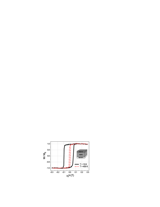
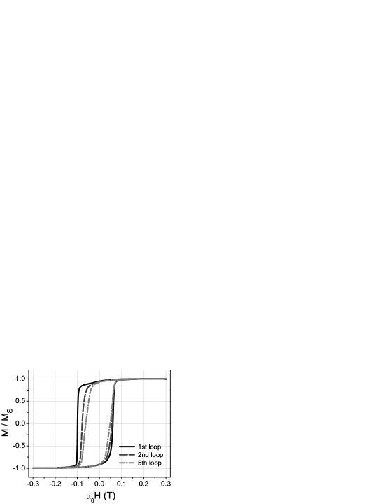
Accordingly, the hysteresis loop of the continuous NiO/Ni film was measured at 10 K after field cooling from 400 K in a field of 0.3 T. The field was applied along the easy axis and its value exceeded the saturation magnetization. In Fig. 4 the resulting data are displayed, together with the hysteresis loop for the non-EB case, measured at 400 K, i.e., above the blocking temperature. After field cooling, the continuous NiO/Ni sample exhibits an EB field of mT, and the hysteresis loop reveals a slight asymmetry in the ascending and descending branches: The lower right part of the hysteresis is more rounded than the upper left part. Due to this observation, we analyzed the training effect of the EB system. In Fig. 5 the virgin hysteresis loop and the magnetization reversal for the second and the fifth cycle are shown, again measured at 10 K after field cooling starting at 400 K. Obviously, only the virgin curve is asymmetric, whereas the trained hysteresis curves are centered around a point on the field axis set by the EB field.
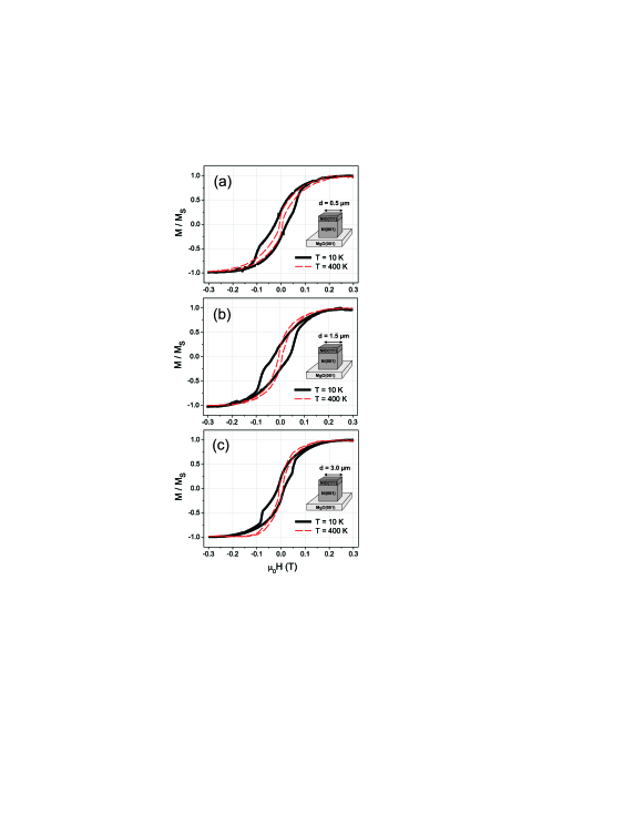
The hystereses for the patterned samples are shown in Fig. 6, where the field was applied along the edges of the squares, i.e., along the easy axis according to the continuous film. The shape of the hysteresis loop at 400 K changed remarkably compared to the continuous NiO/Ni film and clearly indicates a domain state at remanence. Moreover, the magnetic hysteresis loops at 10K (solid lines) show considerable divergence of the shape, coercivity and EB field magnitude from the corresponding data for the continuous NiO/Ni film. It is also noticeable that in the EB case all hysteresis loops of the patterned samples show kinks in each branch before reaching saturation and exhibit an asymmetric shape. However, the shape of the hysteresis loops measured in the non-EB case is symmetric and no kinks are visible. Altogether, the hysteresis loops indicate that in the EB case the square microstructures have a domain configuration similar to a vortex state. In the non-EB case a different remagnetization process is observed, although it should be noted that the loop is slightly more narrow close to remanence than for higher fields.
Another remarkable feature is the behavior of the EB fields given in table 1. For the squares with 0.5 and 3.0 m edge lengths, the EB field is reduced to -1.25 and -0.75 mT, respectively. Surprisingly, for the squares with 1.5 m edge length, the hysteresis is shifted to a positive EB with mT. This positive EB was observed for several samples with squares of 1.5 m edge size, so that we can exclude individual structural and lithographical properties of the sample. The positive EB appears to be related to changes in the remagnetization behavior and it is thus not a fundamentally new feature of EB in microstructures, as described below.
| Edge size of squares | |||
|---|---|---|---|
| (m) | (mT) | (mT) | (mT) |
| Continuous film | -96.5 | +59.0 | -18.75 |
| 3.0 | -14.0 | +12.5 | -0.75 |
| 1.5 | -29.4 | +36.0 | +3.3 |
| 0.5 | -25.0 | +22.5 | -1.25 |
| Edge size of squares | |||
|---|---|---|---|
| (m) | (mT) | (mT) | (mT) |
| Continuous film | -96.5 () | +59.0 () | -18.75 |
| 3.0 | -76.3 | +47.1 | -14.6 |
| 1.5 | -70.7 | +44.3 | -13.2 |
| 0.5 | -90.2 | +55.4 | -17.4 |
IV MICROMAGNETIC SIMULATION
To determine the origin of the vortexlike shaped hysteresis loops, micromagnetic calculations with the OOMMF simulation software package were performed Donahue and Porter (1999). We modeled a square dot with an edge length of 0.5 m consisting of nickel (saturation magnetization MA/m and exchange constant pJ/m). A cubic magnetocrystalline anisotropy footnote1 with the easy axes along [1 1 0], [-1 1 0] and [0 0 1] and an anisotropy constant of kJ/m3 were assumed. The EB field was simulated with locally pinned AF spins distributed randomly across 10% of the area Petracic et al. (2005).
The hysteresis loop obtained from the micromagnetic model when the field is applied along the edge of the structure is shown in Fig. 7(a). The inset shows the simulation result for the non-EB case, where no pinned AF spins are assumed. It is symmetric and no vortex state occurs. The more rounded experimental hysteresis loop is most likely due to the sequential switching of individual dots with a distribution of coercive fields. In the EB case, the hysteresis loop has a characteristic shape resembling the experimental data from Fig. 6. In particular, the narrowing close to the coercive fields and the kinks in the ascending and descending branches of the hysteresis loops are properly reproduced. However, compared to the experimental data, the loop shows a pronounced EB field , and the remagnetization process occurs within a rather small field range. As previously shown, we attribute this deviation to the spin-glass behavior of the interface between the F and the AF layer. It implies that some of the spins at the interface are frozen in and contribute to the EB shift, while others reverse concurrently with the F layer, as soft x-ray resonant magnetic scattering (XRMS) experiments documented Radu et al. (2006). If the latter behavior of the interface spins is taken into account, the hysteresis loop of the EB system broadens and the EB field is reduced, as shown by numerical calculations Radu and Zabel (2008). For the micromagnetic model employed in this paper, these features of the interface spins are not considered, which describes the deviation between the simulated and experimental magnetization reversals qualitatively.
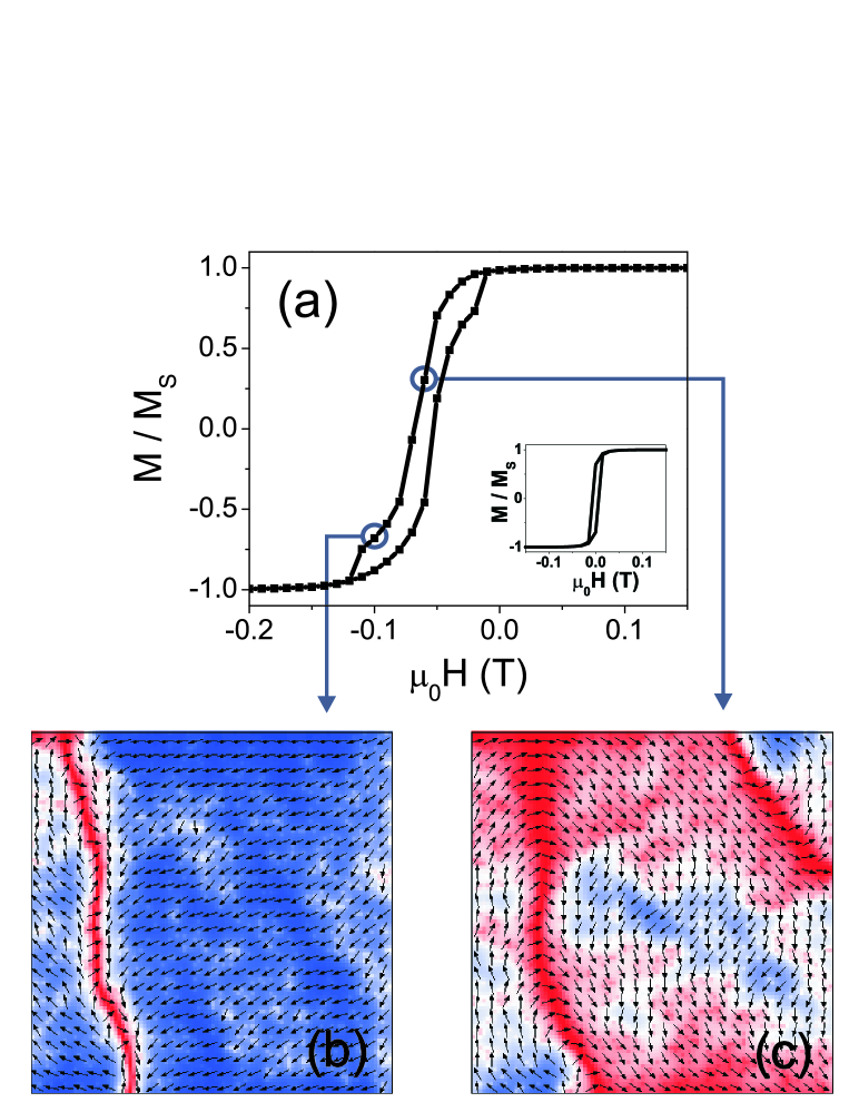
For two characteristic points of the hysteresis loop the domain configuration is displayed in Fig. 7. For the more narrow parts of the hysteresis loop close to remanence domain configurations as in Fig. 7(c) occur, which contain vortexlike states. The kinks emerge due to the collapse of the vortexlike states and the formation of a 360∘ domain wall across the square structure [Fig. 7(b)].
In the simulation we could also see that vortexlike hysteresis loops only arise if a certain balance between the values of the EB field and the shape anisotropy energy exists. By varying either the unidirectional anisotropy strength or the structure size in the set of simulation parameters, we obtained hysteresis loops, which resemble all of those displayed in Fig. 6, apart from an overall shift along the field axis. We observed hysteresis loops with kinks located symmetrical to the hysteresis’s center, but at different field values. Moreover, the positions of the kinks can move such that the upper and the lower kink are encountered at fields asymmetrical to the center of the hysteresis. This might explain the appearance of a positive EB field, being due to a kink forming in the ascending hysteresis branch at the coercive field, but at a different field in the descending branch. However, in the simulation, these features show only a qualitative agreement with the hysteresis loops shown in Fig. 6. In particular, the varying EB field leads to a nonconstant shift of the hysteresis loop. As before, we attribute these deviations to spin disorder at the NiO/Ni interface.
V DISCUSSION
V.1 Continuous NiO/Ni film
For the continuous NiO/Ni film, the shape of the first hysteresis loop (virgin state) is typical of a reversal through nucleation of domain walls and domain wall motion. The second and subsequent reversals indicate that a reversal through rotation of magnetization occurs. For CoO/Co EB systems, the asymmetric shape of the first hysteresis loop has been observed before in, e.g., Refs. Radu et al. (2003) and McCord et al. (2003), where the formation of magnetic domains at the interface subsequent to the first magnetization reversal was reported. In theoretical studies, this training effect was related to irreversible changes taking place during the first reversal at the F/AF interface and in the AF layer Hoffmann (2004); Binek (2004); Radu and Zabel (2008). A more thorough review of the training effect within EB models is given in Ref. Radu and Zabel (2008), including the spin-glass model of EB, which is able to explain many of the observed experimental features associated with the training effect of EB in continuous bilayers.
V.2 Square microstructures
The hysteresis loops in the EB case differ considerably from those in the non-EB case. After the field-cooling procedure, the hysteresis loops exhibit kinks before reaching saturation and the EB field is reduced. This tightening of the hysteresis at coercivity is a feature reminiscent of a vortex state Cowburn et al. (1999). However, in contrast to vortex states in circular islands, the squares appear not to have a well defined nucleation field.
Modified magnetization reversal processes for EB patterns, as compared to continuous exchange biased films, were previously reported. E.g., Eisenmenger et al. Eisenmenger et al. (2005) reported on strongly asymmetrically shaped hysteresis loops of exchange biased Fe/FeF2 circular nanostructures. In a study by Li et al. Li et al. (2005) a vortex state within exchange biased Fe/FeF2 nanostructures was identified by combined SQUID investigations and micromagnetic simulations. The hysteresis loops above the Néel temperature resemble those in the EB case strongly. Kato et al. Kato et al. (2002) imaged square MnIr(20 nm)/NiFe(20 nm) and NiFe(20 nm) nanostructures with MFM that exhibit closure domains. But closure domains for the MnIr/NiFe structures were only found when the corresponding NiFe element also showed a closure domain. This is consistent with the intuitive argument that an additional contribution from unidirectional anisotropy should destroy the highly symmetrical vortex state.
However, this argument does not hold for the patterned samples studied here. Both in the micromagnetic simulation and in the experimental data the vortex states are only present in the EB case but not in the non-EB case. Thus, the change in the magnetization reversal including the kinks in the hysteresis loops must be due to the additional energy contribution from unidirectional anisotropy. As can be seen from the micromagnetic simulation, the local EB acts as a nucleation center for several vortices within the squares with 0.5 m edge length. A similar behavior is expected for the other patterned samples. Moreover, from the numerical calculations, it becomes evident that the balance between shape and unidirectional anisotropy is crucial for the position of the kinks. This is consistent with the observation for the square islands with 1.5 m edge length, where the kinks are not symmetrical to the center of the hysteresis. Additionally to the effects on the shape, the EB field pushes the whole vortexlike hysteresis loop to the negative side of the field axis, acting similarly as in a continuous film. Thereby, the kinks are not encountered at positions equally distant to zero field any more.
Related to the remagnetization behavior is the positive EB field found for the NiO/Ni islands with 1.5 m edge length. A positive EB has been seen before in continuous films and is usually attributed to uncompensated frozen-in spins in the AF layer, which align parallel to the field direction in high enough external fields. For EB islands, a positive shift should rather be related to the shape change in the hysteresis. With a variation of the size of the patterns, the shape anisotropy also changes. As a result of the interplay between shape and unidirectional anisotropy, the hysteresis loop is then different in shape. Especially if the kinks are encountered at positions not symmetrical to the center of the hysteresis, as is the case for the islands with 1.5 m edge length, the coercive fields are affected. Considering that on the length scale discussed the unidirectional anisotropy strength should remain constant, as discussed below, the shape anisotropy should therefore cause the positive EB.
Consequently, with the magnetization reversal being determined by shape anisotropy, it is misleading to use the classical formula for the EB field and relate it to the unidirectional anisotropy energy in the system Hovorka et al. (2006). In the classical EB formula only the coercive fields of the ascending and descending branches and are considered. We propose to use the field position of the kinks to describe possible shifts of the hysteresis. This appears to be a more appropriate procedure to determine the unidirectional anisotropy energy, since the kinks of a typical vortex hysteresis loop have equal distance to the center of the hysteresis. Although multivortex states develop in the samples, which leads to deviations from hysteresis loops typical of a single vortex state, this procedure results in an almost constant EB field, as shown in table 2. The values for the EB field in the table were determined by averaging the field axis values of the left and right kinks. Furthermore, the value of the EB field for the continuous film determined by the classical EB formula is comparable to the EB fields for the patterned samples as obtained by averaging over the positions of the kinks. This indicates that the unidirectional anisotropy energy is constant for the different samples, which is in agreement with the fact that the AF domain size in the system studied should be rather small Radu et al. (2008); Fraune et al. (2006). Thus, the local EB at the F/AF interface is not affected by the patterning process down to 0.5 m and the unidirectional anisotropy energy remains constant for all the samples. However, the combination of local EB and shape anisotropy has a dramatic effect on the shape of the hysteresis in NiO/Ni microstructures.
VI SUMMARY AND CONCLUSION
We investigated the EB effect in NiO/Ni micro- and submicrostructures. Due to the interplay between shape and unidirectional anisotropy several interesting effects arise. First, vortex formation is more distinctive in the exchange biased square islands than in the corresponding unbiased F islands. Second, the shape of the whole hysteresis is affected by a combination of unidirectional anisotropy and shape anisotropy. Third, as a consequence, the classical formula for the EB field is not appropriate for the description of EB in structures containing a vortex state. Misleading positive EB fields may result from this. A modified procedure for evaluating the EB field is proposed, which takes the change of the shape into account.
ACKNOWLEDGEMENT
We would like to thank T. Eimüller, F. Radu, A. Remhof, P. Szary, and K. Westerholt for helpful discussions. This work was supported by SFB 491 of the Deutsche Forschungsgemeinschaft: ”Magnetic Heterostructures: Spinstructure and Spintransport”, which is gratefully acknowledged.
References
- Meiklejohn and Bean (1956) W. H. Meiklejohn and C. P. Bean, Phys. Rev. 102, 1413 (1956).
- Nogués and Schuller (1999) J. Nogués and I. K. Schuller, J. Magn. Magn. Mat. 192, 203 (1999).
- Kiwi (2001) M. Kiwi, J. Magn. Magn. Mat. 234, 584 (2001).
- Stamps (2000) R. Stamps, J. Phys. D: Appl. Phys. 33, R247 (2000).
- Berkowitz and Takano (1999) A. Berkowitz and K. Takano, J. Magn. Magn. Mat. 200, 552 (1999).
- Radu and Zabel (2008) F. Radu and H. Zabel, Springer Tracts in Modern Physics 227, 97 (2008).
- Nogués et al. (2005) J. Nogués, J. Sort, V. Langlais, V. Skumryev, S. Suriñach, J. S. Muñoz, and M. D. Baró, Phys. Rep. 422, 65 (2005).
- Eisenmenger et al. (2005) J. Eisenmenger, Z.-P. Li, W. A. A. Macedo, and I. K. Schuller, Phys. Rev. Lett. 94, 057203 (2005).
- Popova et al. (2005) E. Popova, H. Loosvelt, M. Gierlings, L. H. A. Leunissen, R. Jonckheere, C. Van Haesendonck, and K. Temst, Eur. Phys. J. B 44, 491 (2005).
- Li et al. (2005) Z.-P. Li, O. Petracic, J. Eisenmenger, and I. K. Schuller, Appl. Phys. Lett. 86, 072501 (2005).
- Sort et al. (2005) J. Sort, A. Hoffmann, S.-H. Chung, K. S. Buchanan, M. Grimsditch, M. D. Baró, B. Dieny, and J. Nogués, Phys. Rev. Lett. 95, 067201 (2005).
- Kato et al. (2002) T. Kato, K. Suzuki, S. Tsunashima, and S. Iwata, Jpn. J. Appl. Phys. 41, L1078 (2002).
- Lukaszew et al. (2005) R. A. Lukaszew, M. Mitra, Z. Zhang, and M. Yeadon, Eur. Phys. J. B 45, 181 (2005).
- Schmitte et al. (2002) T. Schmitte, K. Theis-Bröhl, V. Leiner, H. Zabel, S. Kirsch, and A. Carl, J. Phys.: Condens. Matter 14, 7525 (2002).
- Hwang et al. (2002) H. M. Hwang, I. S. Kim, D. G. You, H. S. Park, M. C. Sung, K. Jeong, J. Lee, T. G. Kim, and J. H. Song, J. Korean Phys. Soc. 41, 114 (2002).
- Roth (1958) W. Roth, Phys. Rev. 110, 1333 (1958).
- Alders et al. (1998) D. Alders, L. H. Tjeng, F. C. Voogt, T. Hibma, G. A. Sawatzky, C. T. Chen, J. Vogel, M. Sacchi, and S. Iacobucci, Phys. Rev. B 57, 11623 (1998).
- Donahue and Porter (1999) M. Donahue and D. Porter, Interagency Report NISTIR 6376, National Institute of Standards and Technology, Gaithersburg (1999).
- (19) Note that the result remains qualitatively similar if [1 1 1], [1 1 -1] and [1 -1 -1] are defined as easy axes, corresponding to the configuration in bulk Ni.
- Petracic et al. (2005) O. Petracic, Z.-P. Li, I. V. Roshchin, M. Viret, R. Morales, X. Batlle, and I. K. Schuller, Appl. Phys. Lett. 87, 222509 (2005).
- Radu et al. (2006) F. Radu, A. Nefedov, J. Grabis, G. Nowak, A. Bergmann, and H. Zabel, J. Magn. Magn. Mater. 300, 206 (2006).
- Radu et al. (2003) F. Radu, M. Etzkorn, R. Siebrecht, T. Schmitte, K. Westerholt, and H. Zabel, Phys. Rev. B 67, 134409 (2003).
- McCord et al. (2003) J. McCord, R. Schäfer, R. Mattheis, and K.-U. Barholz, J. Appl. Phys. 93, 5491 (2003).
- Hoffmann (2004) A. Hoffmann, Phys. Rev. Lett. 93, 097203 (2004).
- Binek (2004) C. Binek, Phys. Rev. B 70, 014421 (2004).
- Cowburn et al. (1999) R. P. Cowburn, D. K. Koltsov, A. O. Adeyeye, and M. E. Welland, Phys. Rev. Lett. 83, 1042 (1999).
- Hovorka et al. (2006) O. Hovorka, A. Berger, and G. Friedman, Appl. Phys. Lett. 89, 142513 (2006).
- Radu et al. (2008) F. Radu, S. Mishra, I. Zizak, A. Erko, H. Dürr, W. Eberhardt, G. Nowak, S. Buschhorn, K. Zhernenkov, M. Wolff, et al., Phys. Rev. B 79, 184425 (2009).
- Fraune et al. (2006) M. Fraune, U. Rüdiger, G. Güntherodt, S. Cardoso, and P. Freitas, Appl. Phys. Lett. 77, 3815 (2000).