Electron Mobility in Silicon Nanowires
Abstract
The low-field electron mobility in rectangular silicon nanowire (SiNW) transistors was computed using a self-consistent Poisson-Schrödinger-Monte Carlo solver. The behavior of the phonon-limited and surface-roughness-limited components of the mobility was investigated by decreasing the wire width from 30 nm to 8 nm, the width range capturing a crossover between two-dimensional (2D) and one-dimensional (1D) electron transport. The phonon-limited mobility, which characterizes transport at low and moderate transverse fields, is found to decrease with decreasing wire width due to an increase in the electron-phonon wavefunction overlap. In contrast, the mobility at very high transverse fields, which is limited by surface roughness scattering, increases with decreasing wire width due to volume inversion. The importance of acoustic phonon confinement is also discussed briefly.
Index Terms:
Silicon nanowires, surface roughness, electron mobilityI Introduction
Akey factor behind the growth of the semiconductor industry for the past 40 years has been the continuous scaling of the device dimensions to obtain higher integration and performance gain. According to the International Technology Roadmap for Semiconductors (ITRS) 2005, the scaling of CMOS technology will continue for at least another decade [1]. Scaling trends also indicate that the devices of the next decade will be quasi-one dimensional (Q1D) nanowires (NW) with spatial confinement along two directions. Due to the compatibility with the existing fabrication facilities, and the superior performance of silicon-on-insulator (SOI) based metal-oxide-semiconductor field effect transistors (MOSFETs) [2], ultra-narrow SOI NWs are expected to play a critical role in future technology nodes. Therefore, it is crucial to accurately model and estimate the performance of these devices.
The low-field electron mobility is one of the most important parameters that determine the performance of a field-effect transistor. Due to the reduced density of states for scattering in 1D structures, the electron mobility in nanowires is expected to increase significantly [3]. Some experimentalists [4, 5] claim to have observed such enhancement of electron mobility in SiNW FETs. But Kotlyar et al. [6] have shown that, in a cylindrical SiNW, the phonon-limited mobility decreases with decreasing diameter due to an increased overlap between the electron and phonon wavefunctions. Recent work also shows that surface roughness scattering (SRS) becomes less important in ultra small SiNWs [7].
In this work, we investigate the mobility of electrons in a rectangular SiNW by taking into account electron scattering due to acoustic phonons, intervalley non-polar optical phonons, and imperfections at the Si-SiO2 interface, and also discuss the importance of incorporating the confinement of acoustic phonons in these structures. Section II describes the device structure used in this study and the components of the simulator employed to calculate the mobility. The simulation results are presented in Section III, while concluding remarks and a brief summary are presented in Section IV.
II Device Structure and Mobility calculation
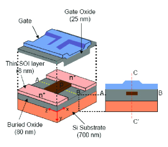
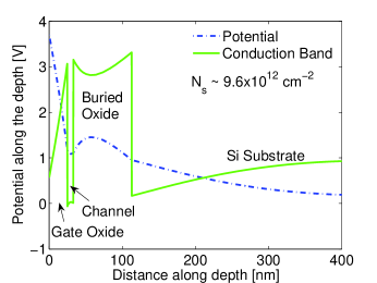
The structure considered in this work is a long, narrow SiNW on ultrathin SOI, similar to the channel of the device depicted in Fig. 1 that was originally proposed by Majima et al [8]. This ultra-narrow SOI MOSFET has a 700 nm silicon substrate, an 80 nm buried oxide, an 8 nm thick SOI layer and a 25 nm gate-oxide. The width of the SiNW in the present simulation is varied from 30 nm to 8 nm, and the channel doping is uniform at . A schematic of the device and the potential profile along the cutline , obtained by self-consistently solving the 2D Poisson and 2D Schrödinger equations, are shown in Fig. 1. The large wire length enables us to approximate it as infinite in the direction of the current flow, so only the carriers’ lateral momenta (and not their positions) need to be updated in the Monte Carlo kernel. The long wire also implies that transport is diffusive (the length exceeds carrier mean free path), which justifies the use of semi-classical Monte Carlo simulation.
As mentioned before, only phonon scattering and surface-roughness scattering are considered in this work. SRS was modeled using Ando’s model [9], and the phonons were treated in the bulk mode approximation. Since the wire is very lightly doped, the effect of impurity scattering was not included. A nonparabolic band model for silicon, with nonparabolicity factor , was used in the calculation of the scattering rates. The details of the simulator and the derivation of 1D scattering rates can be found in Ref. [10]; here, we present only the final expressions used for the scattering rates calculation.
The intravalley acoustic phonon scattering rate, assuming elastic scattering and the equipartition approximation, is given by
| (1) |
where is the acoustic deformation potential, is the crystal density, and is the sound velocity. and are the initial and final subband index, respectively, while and are the corresponding subband energies. is the initial wavevector in the -direction, in which the motion is unconfined; is the initial (parabolic) kinetic energy associated with , and is the final kinetic energy, given by
| (2a) | |||||
| (2b) | |||||
represents the electron-phonon wavefunction overlap integral [6], given by
| (3) |
where and are the electron wavefunctions in subbands and , respectively.
The intervalley non-polar optical phonon scattering rate is given by
| (4) | ||||
where is the optical deformation potential, and is defined in (3). The approximation of dispersionless bulk optical phonons of energy was adopted, where is their average number at temperature . The Heaviside step function ensures the conservation of energy after scattering, so the final kinetic energy in the case of optical phonons is similar to that in the acoustic phonon expression (2b), but with an additional on the right-hand-side to account for the emission/absorption of a phonon of energy .
Assuming exponentially correlated surface roughness [11] and incorporating the wavefunction deformation using Ando’s model [9], the SRS rate is given by
| (5) | ||||
where is given by Eq. (2b), and and are the r.m.s. height and the correlation length of the fluctuation at the Si-SiO2 interface, respectively. To fit the experimental data, = 0.45 nm and = 2.5 nm are used in this work to characterize the SRS due to each of the four interfaces. is the transferred wavevector, where the angle between the initial () and the final () electron wavevector can only be 0 or , corresponding to the in the superscript. The SRS overlap integral in Eq. (5), for the top and bottom interface, is given by
| (6) | ||||
The SRS rate and its corresponding overlap integral for the two side interfaces can be obtained by interchanging and in Eq. (6).
Using the wavefunctions and potential obtained from the self-consistent Poisson-Schrödinger solver, the scattering rates are calculated. The phonon deformation potentials were taken from Ref. [12]. A Monte Carlo transport kernel [13] is used to model electron transport in the unconfined direction under the influence of a very low lateral electric field. The mobility of the electrons in the channel is then calculated from the ensemble average of the electron velocities [13].
III Simulation Results
III-A Validation of the Simulator
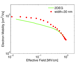
A device with a width of 30 nm [at this width, electrons in the channel feel very weak spatial confinement along the width direction and therefore behave like a two-dimensional electron gas (2DEG)] was used to compare the mobility results obtained from our simulator with the experimental data of Koga et al. [14] for a 2DEG of the same thickness. Fig. 2 shows the calculated low-field electron mobility variation with the transverse effective field. Although there is a good agreement with the experimental data at high fields, we find that the simulator overestimates the mobility in the moderate and low-field regions, where phonon scattering dominates. This discrepancy is due to the bulk phonon approximation used in the calculation of the electron-phonon scattering rates, and a similar result has been reported in ultra-thin SOI structures [15, 16]. The importance of including phonon confinement in the calculation of the electron-phonon scattering rates in nanostructures has previously been established [17, 18]. In ultra-thin and ultra-narrow structures, the phonon spectrum is modified due to the mismatch of the sound velocities and dielectric constants between the wire and the surrounding material [19, 20], in our case – silicon and SiO2. Presently, we are working on incorporating confined acoustic phonons in the calculation of electron-phonon scattering rates in SiNWs, and the results will be presented in a subsequent publication. Even for a relatively wide, 30-nm wire, preliminary results indicate that the acoustic phonon scattering rate is significantly higher when phonon confinement is included in the calculation.
III-B Effect of Decreasing Channel Width
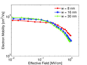
The variation of the field-dependent mobility with decreasing channel width was investigated on a series of SiNWs, while keeping the channel thickness at 8 nm. Fig. 3 shows the mobility for SiNWs with the widths of 30 nm, 16 nm and 8 nm. Two important results regarding the mobility behavior in the width range considered can be deduced from Fig. 3: (i) the mobility at high transverse fields, which is dominated by SRS, increases with decreasing wire width and (ii) the mobility at low-to-moderate transverse fields, determined by phonon scattering, decreases with decreasing wire width.
III-B1 Effect of Bulk Phonon Scattering
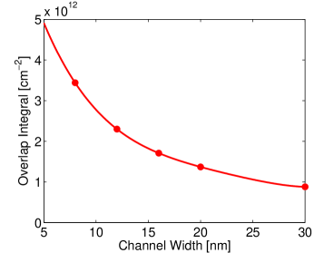
Phonon scattering variation with decreasing wire width is determined by the interplay of two opposing factors: (i) reduction of the final density of states for the electrons to scatter to, and (ii) an increase in the electron-phonon wavefunction overlap (3). The former results in an enhanced mobility, while the latter results in mobility degradation. The overlap integral (3) shown in Fig. 4 for various widths increases with a decrease in the wire width due to an increase in the electron confinement. In narrow wires, the increase in the electron-phonon wavefunction overlap dominates over the density-of-states reduction, resulting in a net decrease in the electron mobility at low-to-moderate transverse fields.
III-B2 Effect of Surface Roughness Scattering
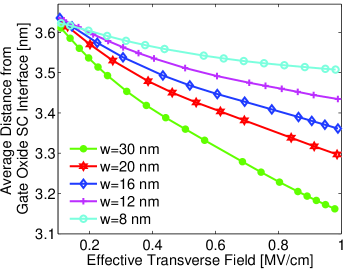
The SRS overlap integral given by (6) has three terms. Two are due to deformation of the wavefunction, and the third, dominant term depends on the strength of the field perpendicular to the interface. Since the field normal to the side interfaces is very weak, SRS due to these interfaces is much less efficient than scattering due to the top and bottom ones. The decrease in SRS with decreasing wire width can be understood by following the behavior of the average distance (7) of the carriers from the top interface:
| (7) |
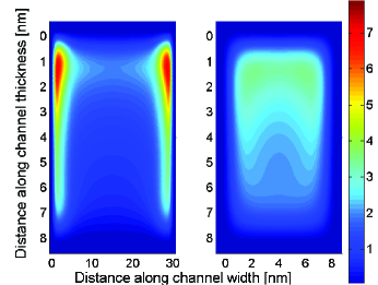
where is the total line density and is the line density in the subband of the valley. In Fig. 6, we can see that the carriers are moving away from the top interface as the width of the wire is decreased, and are therefore not strongly influenced by the interface. This behavior is also observed in the case of ultrathin double-gate SOI FETs, and is due to the onset of volume inversion [21, 22]. As the SiNW approaches the volume inversion limit, carriers cease to be confined to the interfaces, but are distributed throughout the silicon volume. Fig. 6 shows the distribution of carriers in a 30 nm wire and a 8 nm wire at the same effective field; we can clearly see that the carriers are confined extremely close to the interface in the 30 wide nm wire, whereas they are distributed throughout the silicon layer in the case of the 8 nm wire.
IV Conclusion
The transverse-field dependence of the low-field electron mobility in rectangular silicon nanowires was calculated using a self-consistent 2D Schrödinger-Poisson–1D Monte Carlo simulation. The effects of varying the wire width and the relative importance of phonon scattering and surface roughness scattering were investigated. For widths in the range between 30 nm and 8 nm, the phonon-limited mobility (dominant at low to moderate transverse fields) was found to decrease with decreasing nanowire width, because of the increase in the electron-phonon wavefunction overlap. Surface roughness scattering was found to decrease with decreasing width due to volume inversion. At high transverse fields, volume inversion results in an appreciable mobility enhancement.
References
- [1] ITRS 2005 Edition, Emerging Research Devices, http://www.itrs.net/common/2005ITRS/Home2005.htm , June 2006.
- [2] J. P. Colinge, Silicon-On-Insulator Technology: Materials to VLSI. Boston, MA: Kluwer, 1991.
- [3] H. Sakaki, ”Scattering suppression and high-mobility effect of size-quantized electrons in ultrafine semiconductor wire structures,” Jpn. J. Appl. Phys., vol. 19, no. 12, pp. L735-L738, 1980.
- [4] Y. Cui, Z. H. Zhong, D. L. Wang, W. U. Wang, and C. M. Lieber, ”High performance silicon nanowire field effect transistors,” Nano Lett., vol. 3, no. 2, pp. 149-152, 2003.
- [5] S. M. Koo, A. Fujiwara, J. P. Han, E. M. Vogel, C. A. Richter, and J. E. Bonevich, ”High inversion current in silicon nanowire field effect transistors,” Nano Lett., vol. 4, no. 11, pp. 2197-2201, 2004.
- [6] R. Kotlyar, B. Obradovic, P. Matagne, M. Stettler, and M. D. Giles, ”Assessment of room-temperature phonon-limited mobility in gated silicon nanowires,” Appl. Phys. Lett., vol. 84, no. 25, pp. 5270-5272, 2004.
- [7] J. Wang, E. Polizzi, A. Ghosh, S. Datta, and M. Lundstrom, ”Theoretical investigation of surface roughness scattering in silicon nanowire transistors,” Appl. Phys. Lett., vol. 87, no. 4, 043101, 2005.
- [8] H. Majima, H. Ishikuro, and T. Hiramoto, ”Experimental evidence for quantum mechanical narrow channel effect in ultra-narrow MOSFETs,” IEEE Electron Device Lett., vol. 21, no. 8, pp. 396-398, 2000.
- [9] T. Ando, A. B. Fowler, and F. Stern, ”Electronic propeties of two-dimensional systems,” Rev. Mod. Phys., vol. 54, no. 2, pp. 437-672, 1982.
- [10] E.B. Ramayya, MS Thesis, Arizona State University, May 2006.
- [11] S.M. Goodnick, D.K. Ferry, C.W. Wilmsen, Z. Liliental, D. Fathy, and O.L. Krivanek, ”Surface roughness at the Si(100)-SiO2 interface,” Phys. Rev. B, vol. 32, no. 12, pp. 8171-8186, 1985.
- [12] S. Takagi, J. Koga, and A. Toriumi, ”Mobility enhancement of SOI MOSFETs due to subband modulation in ultrathin SOI films,” Jpn. J. Appl. Phys., vol. 37, no. 3B, pp. 1289-1294, 1998.
- [13] C. Jacoboni and L. Reggiani, ”The Monte Carlo method for the solution of charge transport in semiconductors with applications to covalent materials,” Rev. Mod. Phys., vol. 55, no. 3, pp. 645-705, 1983.
- [14] J. Koga, S. Takagi, and A. Toriumi, ”Influences of buried-oxide interface on inversion-layer mobility in ultra-thin SOI MOSFETs,” IEEE Trans. Electron Devices, vol. 49, no. 6, pp. 1042-1048, 2002.
- [15] L. Donetti, F. Gamiz, J. B. Roldan, and A. Godoy, ”Acoustic phonon confinement in silicon nanolayers: Effect on electron mobility,” J. Appl. Phys., vol. 100, no. 1, 013701, 2006.
- [16] L. Donetti, F. Gamiz, N. Rodriguez, F. Jimenez, and C. Sampedro, ”Influence of acoustic phonon confinement on electron mobility in ultrathin silicon on insulator layers,” Appl. Phys. Lett., vol. 88, no. 12, 122108, 2006.
- [17] S. Yu, K. W. Kim, M. A. Stroscio, G. J. Iafrate, and A. Ballato, ”Electron-acoustic-phonon scattering rates in rectangular quantum wires,” Phys. Rev. B, vol. 50, no. 3, pp. 1733-1738, 1994.
- [18] A. Svizhenko, S. Bandyopadhyay, and M. A. Stroscio, ”The effect of acoustic phonon confinement on the momentum and energy relaxation of hot carriers in quantum wires”, J. Phys.: Condens. Matter, vol. 10, pp. 6091-6104, 1998.
- [19] E. P. Pokatilov, D. L. Nika and A. A. Balandin, ”Acoustic phonon engineering in coated cylindrical nanowires,” Superlattices Microstruct., vol. 38, no. 3, pp. 168-183, 2005.
- [20] E. P. Pokatilov, D. L. Nika and A. A. Balandin, ”Acoustic-phonon propagation in rectangular semiconductor nanowires with elastically dissimilar barriers,” Phys. Rev. B, vol. 72, 113311, 2005.
- [21] F. Balestra, S. Cristoloveanu, M. Benachir, J. Brini, and T. Elewa, ”Double-gate silicon-on-insulator transistor with volume inversion - a new device with greatly enhanced performance,” IEEE Electron Device Lett., vol. 8, no. 9, pp. 410-412, 1987.
- [22] F. Gamiz and M. V. Fischetti, ”Monte Carlo simulation of double-gate silicon-on-insulator inversion layers: The role of volume inversion”, J. Appl. Phys., vol. 89, no. 10, pp. 5478-5487, 2001.