Crystallographic Etching of Few-Layer Graphene
Abstract
We demonstrate a method by which few-layer graphene samples can be etched along crystallographic axes by thermally activated metallic nanoparticles. The technique results in long (1 m) crystallographic edges etched through to the insulating substrate, making the process potentially useful for atomically precise graphene device fabrication. This advance could enable atomically precise construction of integrated circuits from single graphene sheets with a wide range of technological applications.
Due to its remarkable electronic properties, few layer graphene is emerging as a promising new material for use in a vast array of postsilicon nanoelectronic devices incorporating quantum size effects.1,2 Of particular interest would be the construction of atomically precise graphene nanoribbons, in which charge carriers are confined in the lateral dimension whereby the electronic properties are controlled by the width and specific crystallographic orientation of the ribbon.3-14 Such structures hold enormous promise as nanoscale devices similar to those recently developed using carbon nanotubes2,11,15 with the added advantage that graphene s two-dimensionality lends itself to existing device architectures based on planar geometries.
However, these structures have so far been impossible to achieve because of the rough noncrystalline edges of the graphene that result from current state-of-the-art nanolithography techniques.2,16,17 These rough edges are thought to be the crucial limiting factor to attaining useful performance and on/off current ratios from nanoscale graphene devices.13,18,19
As a step toward band gap engineering of this material, we have developed a means by which few-layer graphene (FLG) samples can be etched along crystallographic axes by thermally activated metallic nanoparticles.20 The technique results in long (1 m) trenches commensurate with the crystal lattice that are etched through to the supporting insulating substrate, making the process potentially useful for atomically precise graphene device fabrication, as well as indicating a possible method by which entire circuits could be carved out from single graphene sheets.1
Our initial samples (before etching) consisted of pristine few-layer graphene sheets transferred onto highly doped Si substrates with 300 nm thermally grown SiO2 by mechanical exfoliation under ambient conditions, similar to the technique described in ref 21. Flakes of few-layer graphene are identified using optical microscopy. Height imaging of our samples is done using a Veeco Dimension 3100 atomic force microscope (AFM) operating in intermittent contact mode, with Si3N4-coated tips (NSC15, Mikromasch) of curvature radius 20 nm. Samples are also characterized using a JEOL JSM6400 scanning electron microscope (with a LaB6 filament).
The FLG on SiO2/Si substrates are uniformly spin-coated with 15 mL solution of 50 mg/L Fe(NO3)9H2O in isopropyl alcohol (HPLC grade). The samples are then transferred to a furnace and heated in hydrogen and argon gas coflow (320 sccm/600 sccm, respectively) at 900∘C for 45 min. At these temperatures, the Fe accumulates to form small 15 nm diameter nanoparticles which can diffuse along the surface of the SiO2 and graphene.22 As the nanoparticles diffuse over the surface of the SiO2 and graphene at these elevated temperatures, they etch away the FLG sheets.
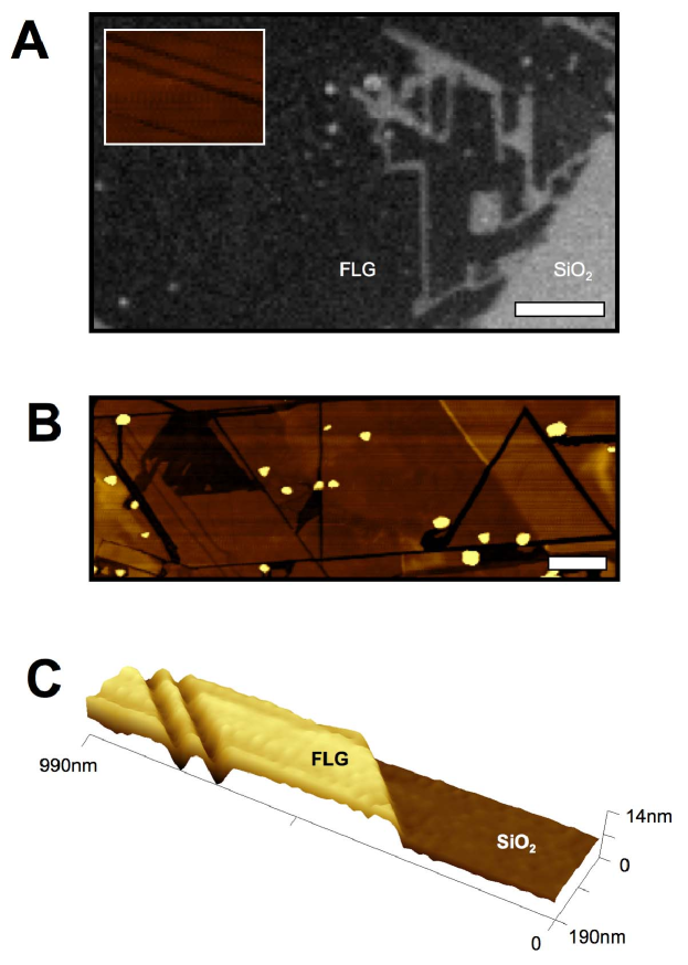
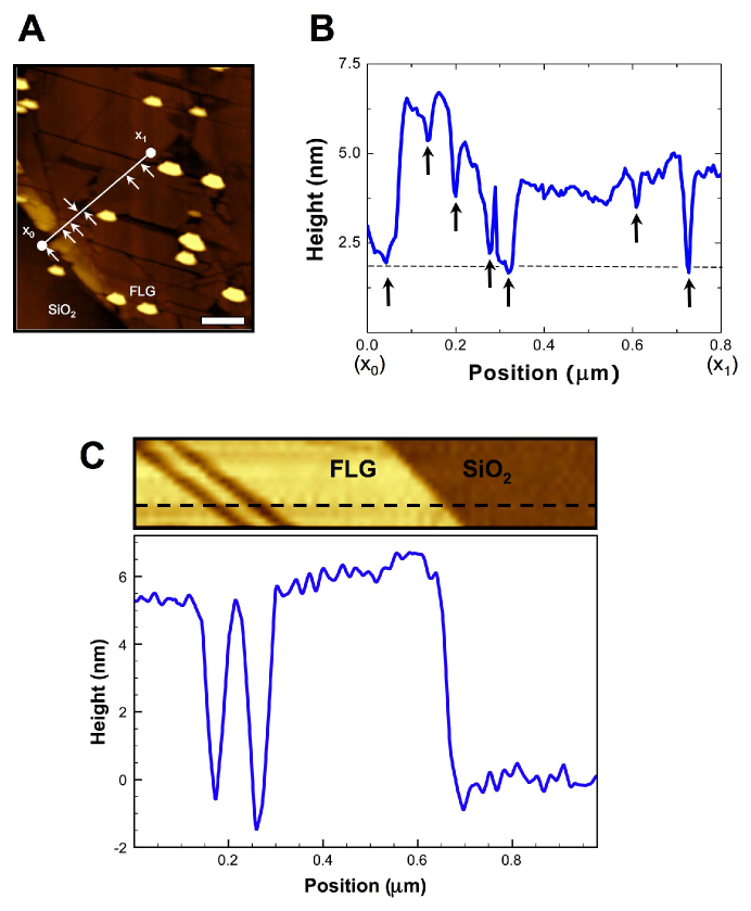
Figure 1 shows AFM and SEM images of FLG samples after this etching procedure. Crucially, we observe long and straight (1 m) nanotrenches in the FLG along which graphene has been removed. The majority of these trenches are etched down to the insulating substrate. This is evident through contrast variations in SEM images and through detailed AFM height analysis of the nanotrenches (Figure 1). We find through cross-section analysis (as in Figure 2) that the depths of the trenches correspond to the difference in height between the bare substrate and the FLG flake. This indicates that the trench forming process results in tracks that are etched down to the insulating substrate. AFM imaging shows that the graphene surface has roughness on the order of 0.5 nm, which is the roughness of the substrate and is consistent with our and others measurements of the intrinsic roughness of FLG on SiO2:23 this indicates that the graphene surface is largely unspoiled by the etching procedure. AFM analysis also reveals that the widths of the trenches are on the order of tens of nanometers and frequently less than 20 nm. In the AFM images, some narrow trenches do not appear to extend down to the underlying substrate which can be due to the fact that they are not fully resolved when they are narrower than the 20 nm wide AFM tip.
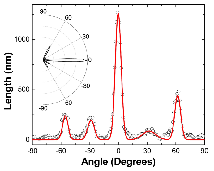
Measurements of the lengths and orientations of etched FLG trenches reveal striking correlations with the graphene lattice. Figure 3 shows a histogram of total etched trench length versus angle for the FLG sample of Figure 2A. Typically, particle tracks travel predominantly along a single direction (defined as 0∘ in Figure 3) with other preferred directions at 60∘ relative to this. Slightly less preferred directions at 30∘ intervals are also observed. It is currently not clear why a single etching direction is preferred. In addition, we note that no significant correlation was found between the orientation of the etched nanotrenches and the direction of gas flow. The existence of these track directions spaced at 30∘ intervals gives strong support to the notion that the etched trenches are commensurate with the graphene honeycomb lattice; thus, our etching procedure could be potentially useful in constructing device edges that are oriented with the underlying crystal lattice of the graphene. This is in contrast to conventional nanolithography etching of FLG samples, which do not yield structures that are commensurate with the graphene lattice. While investigations of the atomic-scale details of our etched graphene edges are still underway, the observed long (on the order of a micrometer) trenches suggest that the edges have long-range order. In addition to other structures, we have used this single-particle etching technique to fabricate graphene nanoribbons of widths measured using AFM as small as 15 nm and lengths on the order of micrometers (e.g., inset to Figure 1A).
FLG etching with metallic nanoparticles likely occurs by a hydrogenation mechanism similar to that studied by numerous researchers several decades ago for bulk carbon allotropes (e.g., ref 20). This reaction, catalyzed by the Fe nanoparticles, is given by
| (1) |
in which the graphene acts as the carbon source C(s). Further evidence that this reaction is the source of the crystallographic etching is found from experiments performed in hydrogen-free argon gas flow which do not result in nanotrench formation.24
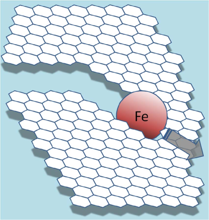
As the Fe particles diffuse on the SiO2 surface, they react with active carbon atoms at the graphene edges. This initiates nanotrench formation, and the moving Fe nanoparticles remove carbon atoms in the graphene along tracks aligned with the underlying crystal lattice, forming the observed nanotrenches (Figure 4). Indeed, we observe that the vast majority of etched trenches commence from the edges of the FLG sheets, with an Fe nanoparticle at the end of each trench. Furthermore, isolated nanoparticles are sometimes observed on top of FLG flakes without any etch track, indicating that carbon atoms at FLG edges (versus those on the FLG surface) are reactive and more likely to initiate nanotrench formation.
The fact that the etching occurs as the nanoparticles move over an amorphous SiO2 surface indicates that the crystallographic orientation of the trenches are determined from the interfacial interactions of the nanoparticle with the edge of the FLG. This crystallographic etching could be due to the favorable adhesion and wetting of the Fe nanoparticles to the graphene edge along specific crystallographic directions.25 Another potential mechanism for our crystallographic etching technique is crystallographic dependence of the Fe-graphene reactivity, for example, due to lowered activation energy of the reaction given in eq 1 along specific directions commensurate with the FLG lattice.20,26
In conclusion, we have demonstrated a technique by which few-layer graphene can be etched along crystallographic directions down to the underlying substrate, a potentially useful technique for attaining further progress in the development of graphene nanoelectronic devices. This technique relies on the use of individual metal nanoparticles as catalysts to “carve out” long, straight nanotrenches with crystallographically oriented edges in FLG samples. The future development of techniques whereby the motion of the nanoparticles can be controlled will lead to possible exciting new graphene device architectures. This could enable the construction of integrated transistors, circuits, chemical sensors, and spin valves from single graphene sheets with many far-reaching potential applications.1
Acknowledgment
This work was supported by the Nano/Bio Interface Center through the National Science Foundation NSEC DMR-0425780 and the JSTO DTRA, the Army Research Office Grant W911NF-06-1-0462, and the Intelligence Community Postdoctoral Fellowship Program.
References
-
1.
Geim, A. K.; Novoselov, K. S. Nat. Mater. 2007, 6, 183 191.
-
2.
Avouris, P.; Chen, Z.; Perebeinos, V. Nat. Nanotechnol. 2007, 2, 605 615.
-
3.
Ezawa, M. Phys. Rev. B 2006, 73, Art. No. 045432.
-
4.
Son, Y.-W.; Cohen, M. L.; Louie, S. G. Phys. Rev. Lett. 2006, 97, Art. No. 216803.
-
5.
Brey, L.; Fertig, H. A. Phys. Rev. B 2006, 73, Art. No. 235411.
-
6.
Shemella, P.; Zhang, Y.; Mailman, M.; Ajayan, P. M.; Nayak, S. K. Appl. Phys. Lett. 2007, 91, Art. No. 042101.
-
7.
Son, Y.-W.; Cohen, M. L.; Louie, S. G. Nature 2006, 444, 347 349.
-
8.
Nakada, K.; Fujita, M.; Dresselhaus, G.; Dresselhaus, M. S. Phys. Rev. B 1996, 54, 17954 17961.
-
9.
Wakabayashi, K.; Fujita, M.; Ajiki, H.; Sigrist, M. Phys. Rev. B 1999, 59, 8271 8282.
-
10.
Peres, N. M. R.; Neto, A. H. C.; Guinea, F. Phys. Rev. B 2006, 73, Art. No. 195411.
-
11.
Ouyang, Y.; Yoon, Y.; Fodor, J. K.; Guo, J. Appl. Phys. Lett. 2006, 89, Art. No. 203107.
-
12.
Barone, V.; Hod, O.; Scuseria, G. E. Nano Lett. 2006, 6, 2748 2754.
-
13.
Areshkin, D. A.; Gunlycke, D.; White, C. T. Nano Lett. 2007, 7, 204 210.
-
14.
Hod, O.; Barone, V.; Peralta, J. E.; Scuseria, G. E. Nano Lett. 2007, 7, 2295 2299.
-
15.
Obradovic, B.; Kotlyar, R.; Heinz, F.; Matagne, P.; Rakshit, T.; Giles, M. D.; Stettler, M. A.; Nikonov, D. E. Appl. Phys. Lett. 2006, 88, 142102.
-
16.
Chen, Z.; Lin, Y.-M.; Rooks, M. J.; Avouris, P. Physica E 2007, 40, 228 232.
-
17.
Han, M. Y.; Ozyilmaz, B.; Zhang, Y.; Kim, P Phys. Rev. Lett. 2007, 98, Art. No. 206805.
-
18.
Basu, D.; Gilbert, M. J.; Register, L. F.; MacDonald, A. H.; Banerjee, S. K. Appl. Phys. Lett. 2007, 92, 042114.
-
19.
Li, T. C.; Lu, S.-P. Phys. Rev. B 2008, 77, 085408.
-
20.
Tomita, A.; Tamai, Y. J. Phys. Chem. 1974, 78, 2254 2258.
-
21.
Novoselov, K. S.; Geim, A. K.; Morozov, S. V.; Jiang, D.; Zhang, Y.; Dubonos, S. V.; Grigorieva, I. V.; Firsov, A. A. Science 2004, 306, 666 669.
-
22.
Klinke, C.; Bonard, J.-M.; Kern, K. J. Phys. Chem. B 2004, 108, 11357 11360.
-
23.
Ishigami, M.; Chen, J. H.; Cullen, W. G.; Fuhrer, M. S.; Williams, E. D. Nano Lett. 2007, 7, 1643.
-
24.
Methane formation in the reaction given by eq 1 could occur either by dissociation and dissolution of molecular hydrogen in the Fe nanoparticle and subsequent hydrogen reaction with carbon atoms at the metal-graphene interface or, as is more likely, by dissolution of carbon atoms from the metal-graphene interface through the Fe nanoparticles and subsequent reaction with hydrogen at the Fe surface.
-
25.
de Gennes, P. G.; Brochard-Wyart, F.; Quere, D. Capillary and Wetting Phenomena – Drops, Bubbles, Pearls, Waves; Springer: New York, 2002.
-
26.
Thomas, J. M., Chemistry and Physics of Carbon; Marcel Dekker: New York, 1965; Vol. 1.


