Test Beam Characterizations of 3D Silicon Pixel Detectors
Abstract
3D silicon detectors are characterized by cylindrical electrodes perpendicular to the surface and penetrating into the bulk material in contrast to standard Si detectors with planar electrodes on its top and bottom. This geometry renders them particularly interesting to be used in environments where standard silicon detectors have limitations, such as for example the radiation environment expected in an LHC upgrade. For the first time, several 3D sensors were assembled as hybrid pixel detectors using the ATLAS-pixel front-end chip and readout electronics. Devices with different electrode configurations have been characterized in a 100 GeV pion beam at the CERN SPS. Here we report results on unirradiated devices with three 3D electrodes per 50400 m2 pixel area. Full charge collection is obtained already with comparatively low bias voltages around 10 V. Spatial resolution with binary readout is obtained as expected from the cell dimensions. Efficiencies of for tracks parallel to the electrodes and of at 15∘ are measured. The homogeneity of the efficiency over the pixel area and charge sharing are characterized.
I Introduction
The silicon tracking devices at the LHC detectors ATLAS and CMS have to cope with very intense radiation levels reaching fluence levels of up to 1015 particles per cm2 in the innermost pixel layer during a ten year LHC projected life time [1]. This large particle fluence causes damage to silicon pixel sensors, most dominantly by: (a) the trapping of moving charges which reduces the signal, (b) an increase in the negative space charge concentration Neff of the depleted silicon bulk which needs a larger external bias voltage to reach full depletion, and (c) an increase of leakage currents due to new energy states inside the band gap. The semiconductor tracking detectors of the large LHC experiments ATLAS and CMS have been designed and built to stand these challenges for the LHC life time [2, 3, 4, 5]. As plans for an upgrade of the LHC which may eventually lead to an increase in luminosity by a factor of 10 (sLHC, Super-LHC) are discussed [6], new types of sensors for pixel detectors, either by material or by design, are being investigated to be able to cope with the concurrent increase also in radiation fluence of up to 1016 particles per cm2. For such radiation levels the present detectors are not suited. So-called 3D-silicon sensors have been proposed and developed ([7, 8] and references therein). Due to a different electrode configuration 3D sensors are more radiation hard and have faster charge collection than standard planar silicon sensors. They are thus a prime candidate for pixel sensors at the sLHC.
II The tested structures
The basic concept of 3D silicon sensors is shown in fig. 1. A 3-dimensional structure is obtained by processing the n+ and p+ electrodes into the substrate bulk by combining VLSI and MEMS (Micro Electro Mechanical Systems) technologies [9]. Charge carriers drift inside the bulk parallel to the surface over a typical drift distance of 50 – 100 m. Typical depletion voltages are of the order of 10 V.
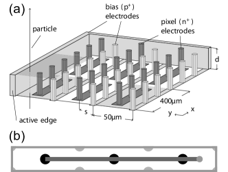
In this paper we have particularly studied the response of 3D pixel devices to high energy particles in terms of response homogeneity and spatial resolution. A wafer with three different types of 3D structures geometrically adapted to fit the pixel pattern of the ATLAS pixel frontend chip FE-I3 [10] has been produced at the Stanford Nanofabrication Facility [11]. The thickness of the p-type sensors is 208 5 m. The nominal etched diameter of the 3D-columns is 17m. PbSn underbump deposition and flip-chipping to bumped FE-I3 chips was done at IZM-Berlin [12, 13]. The pixel area of the FE-I3 chip is 50m400m. Different structures with different distances between the 3D electrodes were produced to fit the FE-I3 pixel dimensions with two (2E), three (3E), or four (4E) equally-spaced electrodes in the area of one electronics pixel. In this paper we report on the study of the configuration with three electrodes (3E, Fig.1). An evaluation of the 2E, 3E, and 4E structures against each other will be the subject of a future publication. The tested devices were still unirradiated. The ATLAS pixel electronics provides zero suppression in the readout with a threshold level for this study of about 3000e-. The electronics noise is about 380e-. Analog information is obtained via the in-pixel measurement of time-over-threshold (ToT) with an approximate resolution of 7 bits [10]. The calibration is approximately linear for signal charges above 5000 e- with one ToT unit corresponding to about 400 e-.
III Test beam setup and environment
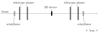
The 3D silicon devices have been tested in a 100 GeV beam of pions at the CERN SPS. The setup is shown schematically in fig. 2. The device under test (DUT, 3D silicon pixels) was placed in between two pairs of silicon microstrip detectors [14]. The telescope was developed for ATLAS and consists of double sided silicon microstrip detectors with 50m pitched strips on both sides rotated by 90∘ with respect to each other. The S/N ratio of about 37 for the p-side, measuring the DUT x-direction, is better than for the n-side (S/N 22), measuring the DUT y-direction. Hits are read out zero suppressed and events waiting for read out can be buffered for some time [14]. The latter option was, however, not used. The setup is triggered by the coincidence signal of two scintillators in front of and behind the setup. The precision obtained in the plane of the DUT is better than 5.3 m in both spatial directions. The beam divergence is measured to be less than 0.2 mrad. The beam incidence angle with respect to the DUT plane is at most 1∘. The average data taking rate was limited by the readout system to around 50-60 Hz. The results presented in this paper concentrate on 3D devices with three electrodes. Bias voltages between 6V and 25V in steps of 4V were applied. Two angles of inclination with respect to the beam, 0∘ and 15∘, were studied.
Only tracks from events with a single hit in each of the telescope planes were selected for characterization measurements. Hits in the 3D-device were accepted if the seed position of the cluster is found in the predicted or in a neighboring pixel. Otherwise they are counted as misses.
IV Results
Operation characteristics
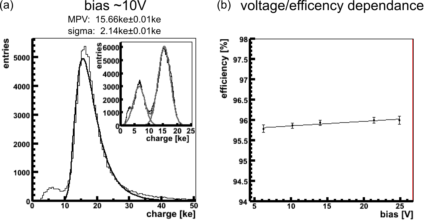
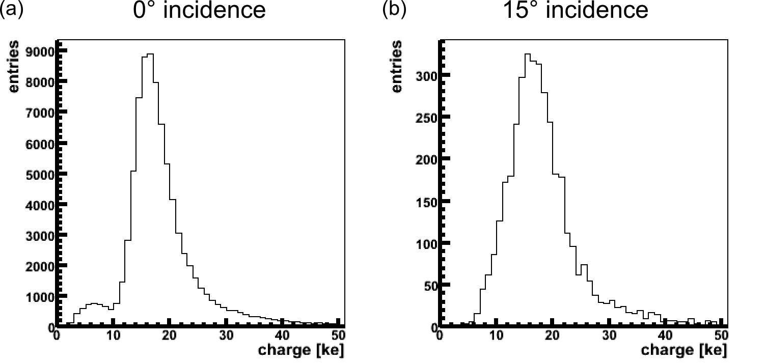
3D devices can be fully depleted with low bias voltages compared to planar silicon sensors. The theoretically expected voltage for cluster signal saturation is about 8 V. In fig. 3(a) the measured charge distribution with a Landau type shape is shown as obtained by operating the DUT with a bias voltage of 10 V. The insert shows the 59.6 keV and 26.3 keV -lines from 241Am, indicating that the ToT calibration uncertainty lies between 5-9. From the fit, the values for peak, mean and sigma for the fully depleted device are 15700 e-, 19200 e- and 2100 e-, respectively, the latter being mostly due to Landau fluctuations. The population of entries at small charges on the left hand side of fig. 3(a) indicate charge losses when tracks pass directly through the 3D-electrodes. This will be studied in more detail below. For data taking the 3D devices were operated with several different bias voltages. We show in fig. 3(b) the hit efficiency, obtained by integrating all hits and misses over the area of a complete pixel cell, as a function of the applied bias voltage. The efficiency is almost unchanged even down to voltages of 6 V. Data using even lower bias voltage were not taken during the test beam. The slight increase with bias voltage seen in fig. 3(b) we interpret as coming from effects due to the higher electric fields inside the sensor rather than being due to a change in the depletion volume.
Hit efficiency
In order to investigate the spatial dependence of the hit efficiency, the sensors with three electrodes per pixel have been scanned with the beam to obtain a hit efficiency map. Scans with straight tracks (perpendicular incidence) and with tracks under an inclination angle of about 15∘ were carried out. For straight track, the obtained efficiency map is shown in fig. 4(a). Tracks from all illuminated pixels enter the efficiency map. The spot-resolution with which the map is drawn is given by the 2-dimensional bin size, smoothed by a gaussian, folded with the telescope extrapolation error. All combined this corresponds to 6.5 m in both coordinates. The position of the 3D electrodes are clearly identified. The overall efficiency for perpendicularly incident tracks, using a threshold setting of 3000 e- and obtained by integrating over the pixel area, corresponds to
| (1) |
The respective cluster charge distribution from the two areas corresponding to low (black central dot in fig. 4(a) and high (ring between radii of 22m and 24m) hit efficiency, are shown separately in figs. 4(b) and (c), properly normalized by area. Note that in fig 4(b) the misses are placed in the first bin and entries at and even somewhat below the nominal threshold of 3000 e- are possible due to the non-linearity of the ToT calibration at small charges. The charge distribution for tracks entering far away from the column center (fig. 4(c)) shows the expected Landau shape with the lowest entries at about 10 ke. Charge entries below 11 ke are thus classified as being due to tracks hitting the region of the 3D electrode.
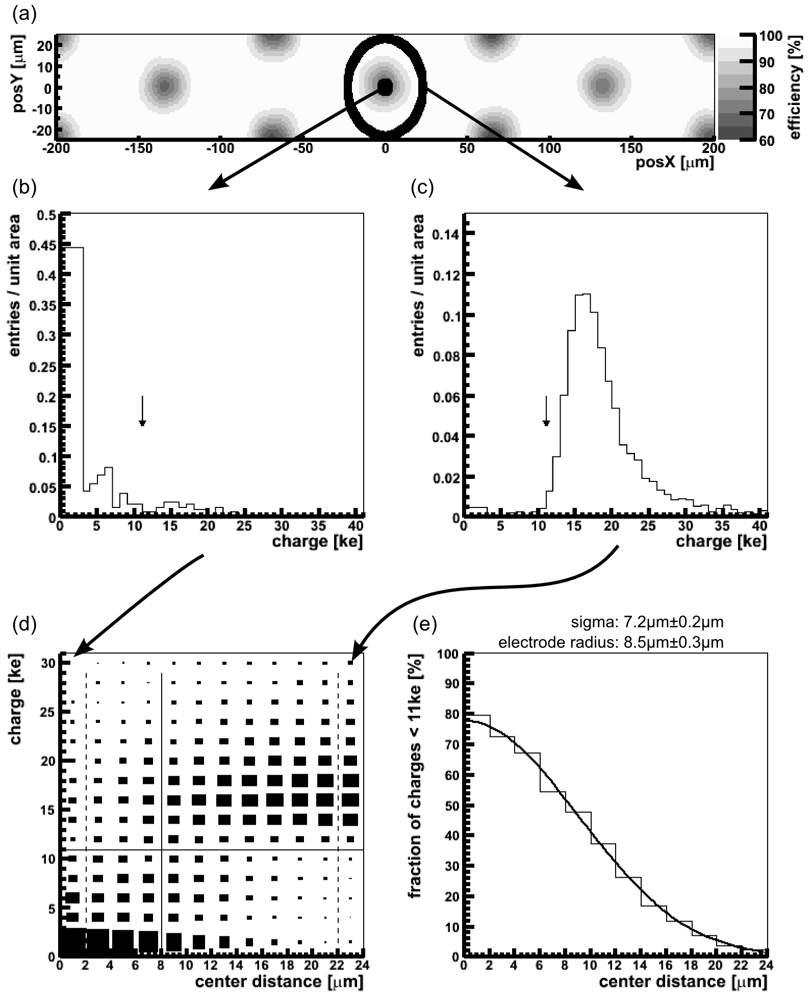
In order to assess the region of reduced efficiency in the 3D-electrodes we plot in fig. 4(d) the measured charge versus the distance R from the nominal center of an electrode column in a 2-dimensional histogram. The solid lines separate regions above and below the low side of the Landau distribution (arrows in fig. 4(c) and (b)), as well as above and below the nominal column etched radius (histogram bin starting at 8 m). In an ideal world this plot would give a discrete charge output (a horizontal line) as a function of . This ideal picture in reality is smeared by (i) the track extrapolation resolution of about 5 m, (ii) the Landau distribution of deposited energy in the sensor, (iii) -electrons being mostly emitted at 90∘ to the tracks and traveling into regions of more/less efficient charge collection, and (iv) the electronics thresholds of 3000 e- existing for every pixel. Figure 4(d) clearly identifies two regions, one with large collected charge at distances larger than about 8 m from the electrode center (upper right), and one with small charge at small distances, corresponding to the column region (bottom left). Figure 4(e), finally, displays the relative fraction of entries in rings around the electrode with a charge smaller that 11 ke, as a function of the distance from the electrode center. The superimposed curve represents a fit of a flat distribution with electrode radius r folded by a Gaussian. In agreement with a simple simulation one finds a column radius of r = (8.50.3) m, in agreement with the with of the nominal etching radius of 8.5 m. The Gaussian is found to be (7.20.2) m, i.e. wider than the contribution from the telescope resolution (5m) alone. Part of this is due to the beam’s 1∘ inclination to the DUT plane, resulting in a 4m space displacement over the depth, but also indicates that the efficiency inside the column is not a step function. The additional spreading we hence interpret as being due to effects like charge diffusion or other mechanisms of signal induction of tracks entering the undepleted column regions.
The mean charge of hits belonging to the region outside of the electrode is about 20 – 25 ke. Hits assigned to the electrode center, on the contrary, show a mean charge below 5ke. Thus, with some uncertainty and caution introduced by the existing pixel thresholds of 3 ke, we estimate the charge collection efficiency inside the 3D-electrode in the order of at most 25%. If, alternatively, one assumes 0 efficiency inside the electrode and 100 outside, the effective column radius is calculated from eq. (1) to be 6.5m.
In a pixel tracking detector, the pixel modules are usually tilted in the azimuthal direction to optimize charge sharing between neighboring readout cells. For 3D sensors this produces the extra beneficial effect that tracks originating from the interaction point would not run exactly parallel through the center of the 3D electrodes. In fig. 5 Landau distributions for perpendicular tracks (0∘) and for tracks under an inclination angle of 15∘ are compared. As expected, for inclined tracks in fig 5(b) the entries with small charge on the left of fig.5(a) disappear. The width of the Landau distribution now broadens by about 20 and shows the lowest detected charge at about 5 ke. While this is beneficial for track detection at collider detectors where tracks always impinge the detector under an angle, the Landau broadening with entries as low as 5 ke does not constitute a comfortable distance to the threshold, in particular when a decrease of the signal charge due to radiation must be expected. The hit efficiency for 15∘ inclined tracks is measured to be
Spatial resolution
The spatial resolution is obtained by plotting the difference between the track position predicted by the telescope on the plane of the DUT (the 3D pixel sensor) and the reconstructed hit of the DUT device. Figure 6 shows this distribution for normal incidence of tracks for both directions of the pixel.
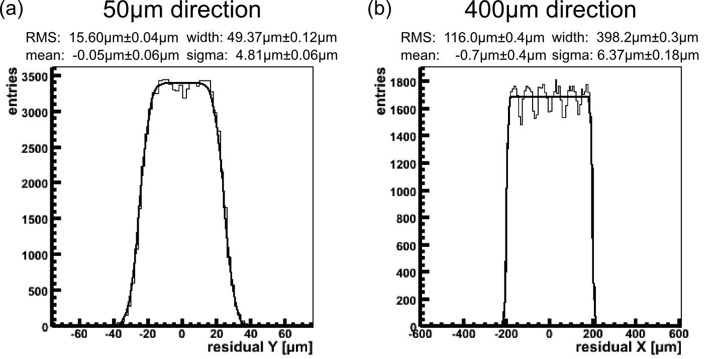
X corresponds to the direction of the long pixel side (400m), Y corresponds to the short direction (50m). For the hit reconstruction first only the digital information is used, i.e. the pixel with the largest signal above threshold collected in a cone around the extrapolated track position is taken as the hit pixel and its center is assumed to be the reconstructed position. The digital resolutions of pixel pitch divided by in both directions, i.e. 14.4 m and 114.5 m are smeared by a Gaussian spread in the order of 5m in y and 6m in x, which is attributed to the resolution of the track extrapolation, the detector noise (380 e-) and the charge sharing behavior of the pixel cells. The structure visible especially in fig. 6(b), results from position dependent response efficiencies which were subject to the investigations above. As will be shown below, charge sharing in 3D sensors is restricted to a very narrow region of about 4m (threshold dependent) at the edge of a pixel. The improvement by using a charge-weighting algorithm (e.g. the so-called -algorithm [15]) compared to a purely digital readout is therefore limited for normally incident tracks. In real vertex detectors charge sharing is usually purposely introduced by tilting the detectors to improve spatial resolution through charge interpolation [16].
Charge sharing
Next we investigate the sharing of charge between pixel cells as a function of the impact point of the track. This is studied by plotting the mean value of the cluster size distribution, where a cluster is a number of nearby hits above threshold. Also the fraction of charge appearing in the pixel with the largest charge of the cluster (seed pixel) is of interest. These quantities are displayed as pixel maps in fig. 7.
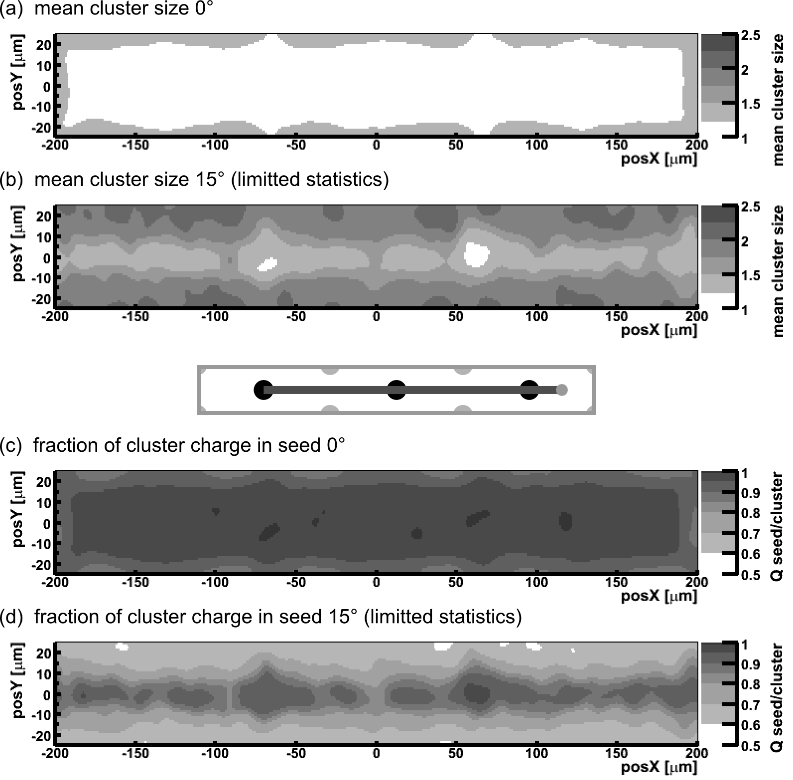
The plots show most clearly the overall expected behavior. On average the cluster size increases for inclined tracks. Correspondingly the seed charge fraction decreases, modulated by the position of the 3D electrodes and the resulting influence on the charge collection efficiency.
V Conclusions
3D active silicon sensors, assembled as pixel devices with the ATLAS front end readout electronics have been tested and characterized for the first time in a high energy (100 GeV) test beam using a 4-plane microstrip beam telescope as reference. Devices with three 3D electrodes under the area of a readout pixel (50400 m2) were characterized. Hit detection efficiencies of () for normal (15∘ inclined) tracks have been obtained. The inefficiencies for normally incident tracks have been identified as being due the presence of the columnar 3D electrodes. For inclined tracks the hit efficiency approaches 100. The spatial distribution of efficiencies and the mean cluster size as well as the fraction of charge seen by the seed pixel, which characterize the charge sharing, have been measured.
Acknowledgments
The authors would like to thank the CERN SPS staff for their help during data taking.
References
- [1] ATLAS Collaboration. The ATLAS Experiment at the CERN Large Hadron Collider. submitted to JINST, 2008.
- [2] ATLAS Pixel Collaboration. ATLAS-Pixel-TDR. CERN/LHCC-98/13, ATLAS-TDR-11, 1998.
- [3] CMS Collaboration. The tracker project – technical design report. CMS TDR 5, CERN/LHCC 98-6, 1998.
- [4] M. S. Alam et al. The ATLAS Silicon Pixel Sensors. Nucl. Inst. and Meth., A456:217–231, 2001.
- [5] K. Arndt, G. Bolla, D. Bortoletto, K. Giolo, R. Horisberger, A. Roy, T. Rohe, and S. Son. Silicon sensors development for the CMS pixel system. Nucl. Inst. and Meth., A511:106–111, 2003.
- [6] see Super-LHC web page. http://care-hhh.web.cern.ch/CARE-HHH/.
- [7] S Parker, C.J. Kenney., and J. Segal. 3-D: A proposed new architecture for solid state radiation detectors. Nucl. Inst. and Meth., A395:328–343, 1997.
- [8] A. Kok et al. 3-D detectors: State of the art. Nucl. Inst. and Meth., pages 127–130, 2006.
- [9] C. Kenney, S. Parker, J. Segal, and C. Storment. Silicon detectors with 3-D electrode arrays: fabrication and initial test results. IEEE Trans. Nucl. Sci., 48, No. 4:1224–1236, 1999.
- [10] G. Comes P. Denes K. Einsweiler P. Fischer E. Mandelli G. Meddeler I. Peric, L. Blanquart. The FEI3 readout chip for the ATLAS pixel detector. Nucl. Inst. and Meth., A565:178–187, 2006.
- [11] Stanford Nanofabrication Facility. weblink: http://snf.stanford.edu.
- [12] J. Wolf, G. Chmiel, and H. Reichl. Lead/tin (95/5 ) solder bumps for flip chip applications based on ti:w(n)/au/cu underbump metallization. In Proc. 5th Intl. TAB/Advanced Packaging Symposium ITAP, pages 141–152, San Jose, USA, 1993.
- [13] J. Wolf. PbSn60 solder bumping by electroplating. In Pixel 2000 Conference, Genova, Italy, June 2000. http://www.ge.infn.it/Pix2000/slides.html.
- [14] J. Treis, P. Fischer, H. Krüger, L. Klingbeil, T. Lari, and N. Wermes. A Modular PC Based Silicon Microstrip Beam Telescope with High Speed Data Acquisition. Nucl. Inst. and Meth., A490:112–123, 2002.
- [15] E. Belau et al. Nucl. Inst. and Meth., A 214:253, 1983.
- [16] G. Aad et al. Atlas pixel detector electronics and sensors. submitted to JINST, 2008.