Method for finding the critical temperature of the island in a SET structure
Abstract
We present a method to measure the critical temperature of the island of a superconducting single electron transistor. The method is based on a sharp change in the slope of the zero-bias conductance as a function of temperature. We have used this method to determine the superconducting phase transition temperature of the Nb island of an superconducting single electron transistor with Al leads. We obtain as high as K and gap energies up to meV. By looking at the zero bias conductance as a function of magnetic field instead of temperature, also the critical field of the island can be determined. Using the orthodox theory, we have performed extensive numerical simulations of charge transport properties in the SET at temperatures comparable to the gap, which match very well the data, therefore providing a solid theoretical basis for our method.
PACS: 73.23.Hk,73.40.Gk,74.50.+r
The single-electron transistor is a device with remarkable properties, which have been intensively studied over the last almost two decades [1]. The first application of such structures have been in the area of electrometry [2], but recently new developments have promoted the superconducting version of this transistor as one of the main contenders for realizing the so-called charge quantum bits [3]. These devices could become the building blocks of future quantum computers, in architectures that allow exchange of quantum information between them via transmission lines [4].
These new areas of interest have created a demand for high performance nanofabrication techniques and there has been a strong motivation to develop a technique for a reliable fabrication of a small niobium-based Josephson junction. Niobium (Nb) would provide more reliable performance in many of these devices due to its large superconducting gap meV (in bulk) as compared to aluminium, meV, which has been the material of choice in nanofabrication for many years due to its easier processability. A larger superconducting gap would provide a better suppression of the undesirable quasiparticle tunnelling and also would yield larger Josephson coupling energy , in ultrasmall junctions.
The conventional e-beam shadow evaporation (self-alignment) technique, has been applied successfully for soft metals like Al, Cu and Pb. Yet, it is known to be difficult to apply this method for refractory metals like Nb due to the poor quality of the produced films, resulting in a critical temperature well below the bulk value. To circumvent this problem, several fabrication methods have been proposed, and different groups have been able to obtain good quality small-capacity single Nb-Al and Nb-Nb junctions [5] and Nb-based single electron transistors [6].
In all these devices, since there is no easy direct electrical access to the island, the typical way to determine the critical temperature is to produce separate samples with films of the same thickness, and measure the critical temperature of those. However, the critical temperature of the Nb island can be quite different from that of a film, since the island’s dimensions are small, comparable with the superconducting coherence length ( nm in the bulk). Of course, determination of the gap at low temperatures from tunneling data provides as well an indirect measure of the critical temperature via the BCS relation: but again, for lower-dimensional superconducting objects the corrections to this law could be significant.
In this article we present a method to determine directly the critical temperature, and also the critical magnetic field, of a Nb island in superconducting Al/AlOx/Nb/AlOx/Al-SETs fabricated with the standard self-alignment lithography process using a slightly modified recipe.
The fabrication technology for our samples has been described elsewhere [5, 7]. The measurements were carried out in a small dilution refrigerator (Nanoway, PDR50) with the base temperature below 100 mK and well-filtered electrical lines.
In Fig. 1(a) we show an SEM picture of one of the samples and its IV characteristic. In the SEM image, brighter lines are niobium and darker lines are aluminium. Besides the existence of a quasiparticle voltage threshold and the Josepshon current, the IV displays a number of features, such as Cooper-pair resonances and low-bias excess currents which have been analyzed elsewhere [7].
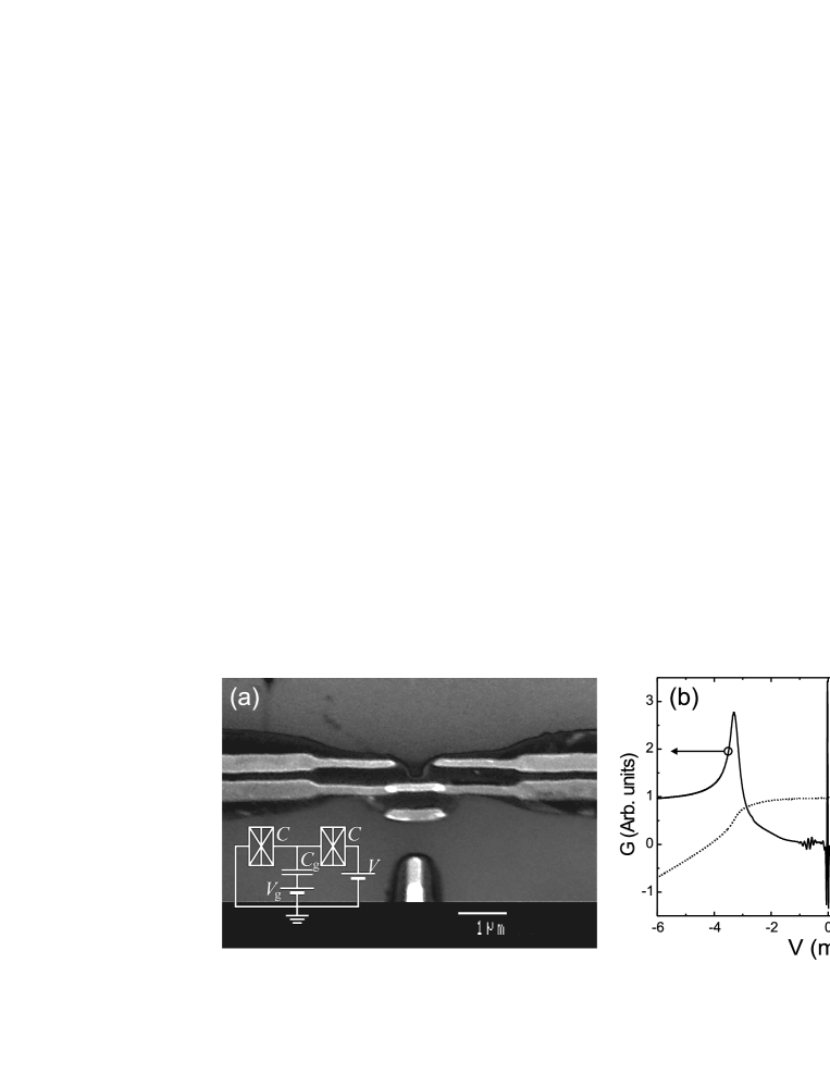
The charging energies of the samples were derived from the normal state conductance curve measured at 4.2 K with magnetic field of T. The obtained charging energies varied between eV. The Josephson coupling energy was found from the Ambegaogar-Baratoff formula for two different superconductors, which yielded eV.
In Fig. 1(b) the - characteristics and a -curve measured at the temperature mK are shown from one of the samples with eV and eV. The gap – with a width of – is clearly visible and the maxima in the -curve yield meV. Here we have assumed meV. At bias voltages below mV we also see (Fig. 1(b), the curve) a series of gate-dependent, equally-spaced peaks, which appear only when the aluminium leads become superconducting. They correspond to Cooper pair resonances occuring when charges are transported in the whole circuit [7].
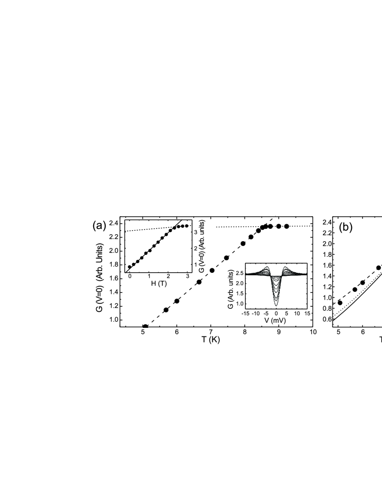
Experimentally, our method consists of determining the critical temperature as well the upper critical field from the zero bias conductance of the sample as a function of temperature or magnetic field, respectively. An example is shown in Fig. 2 where the sudden transition from the strong temperature dependence determined by the reduction in , to a much weaker temperature dependence (due only to Coulomb blockade) is clearly visible at the phase transition. The critical temperatures obtained were 7.8, 8.1 and 8.5 K in the three best samples and above 7.5 K in all others. This is already very close to K in bulk Nb. The obtained critical fields were between T. In this case the transition to the normal state happens gradually between the thermal critical field and the upper critical field where superconductivity is completely suppressed (thin, disordered Nb films are type-II superconductors), as seen on the left inset of Fig. 2(a).
To model or data, we have used the standard orthodox theory [1] for charge transport in NISIN single-electron transistors (at the temperatures of interest, around the critical temperature of Nb, the Al leads are normal). We calculate numerically the tunneling probabilities in each junction for a given superconducting gap, and to find the currents and conductances at a given bias voltage we solve the corresponding master equation for charge transport across the structure for each given temperature. From the low-bias Cooper pair resonance data (which depend on the charging energy) we extract, as in [7], eV. For the gap, which is used to calculate the tunneling probabilities, we use the standard BCS gap equation at finite temperature
where is the density of states at the Fermi level, is the BCS interaction, and the Debye energy is taken much larger than the gap. Since , we can write
an integral equation which is used to determine numerically the gap value at a given temperature T.
Also, when calculating the tunneling probabilities, in order to take into account the excess subgap currents present in Nb-based junctions, we have used a life-time broadening of the quasiparticle energies, resulting in a density of states [7]
| (1) |
where is the probability density associated with a certain value of the gap, where the function is a Gaussian of standard distribution . The value of was determined from this sample using the low-bias plots, as described in [7]: its value is set by the fabrication process and does not depend on temperature. The life-time broadening depends in general on temperature: its value at mK was detemined in [7] as eV. We assume that this dependence is mild near the phase transition so that can be considered constant: we find, as a best fit to the data, eV. We note also that at 5-6 K this value does not give a good fit, and a better match for the data would require indeed a lower value of , corresponding to a lower temperature. Fig. 2(b) summarizes these findings.
We described a new method for determining the critical temperature of a Nb island which forms the active element in a superconducting single electron transistor. The method is based on the experimental observation that, as the system is cycled through the phase transition, the slope of the zero-bias conductance as a function of temperature changes abruptly from a finite value (in the superconducting state) to almost zero (in the normal state).
This work was supported by the Academy of Finland (Projects No. 00857, No. 7111994, and No. 7118122).
References
References
- [1] Grabert H, Devoret M H (eds.) 1992, Single Charge Tunneling (Plenum, New York).
- [2] Schoelkopf R J et. al. 1998, Science 280, 1238; Devoret M H, Schoelkopf R J 2000, Nature 406, 1039
- [3] Nakamura Y, Pashkin Y A, Tsai J S, Nature 1999, 398, 786; Vion D at. al 2002, Science 296, 886; Pashkin Yu. A. et. al. 2003, Nature 421, 823; Yamamoto T et. al. 2003, Nature 425, 941; ; Duty T, Gunnarsson D, Bladh K, Delsing P 2004, Phys. Rev. B 69, 140503(R).
- [4] Blais A 2004 et. al Phys. Rev. A 69, 062320; Wallraff A et. al. 2004, Nature (London) 431, 162; Blais A et. al. 2007, Phys. Rev. A 75, 032329; Paraoanu G S 2006, Phys. Rev. B 74, 140504 (R); Li J, Chalapat K, Paraoanu G S 2008 Entanglement of superconducting qubits via microwave fields: classical and quantum regimes Preprint, arXiv:0803.0397
- [5] Paraoanu G S, Halvari A M 2003, Rev. Adv. Mater. Sci. 5, 292
- [6] Zorin A B, Lotkhov S V, Zangerle H, and Niemeyer J, 2000 J. Appl. Phys. 88, 2665; Dolata R, Scherer H, Zorin A B, Krupenin V A, Niemyer J 2002, Appl. Phys. Lett. 80 2776; Kim N et. al. 2003, Physica B 329-333, 1519; Watanabe M, Nakamura Y, Tsai J-S, Appl. Phys. Lett. 84 410; Savin A M et. al. 2007 Appl. Phys. Lett. 91, 063512
- [7] Toppari J J et. al 2007, Phys. Rev. B 76, 172505