Further author information: (Send correspondence to I.A. E-mail: abdulhlm@bgumail.bgu.ac.il, Telephone: 972 8 646 1448
Porosity Effect on Surface Plasmon Resonance from Metallic Sculptured Thin Films
Abstract
When a sculptured thin film (STF), made of a metal and nm thick, is used in lieu of a dense layer of metal in the Kretschmann configuration, experimental data for an STF comprising parallel tilted nanowires shows that a surface plasmon resonance (SPR) can still be excited. As the porosity of the chosen STF increases, experimental data and numerical simulations indicate the SPR dip with respect to the angle of incidence of the exciting plane wave widens and eventually disappears, leaving behind a a vestigial peak near the onset to the total-internal-reflection regime.
keywords:
Columnar thin film, surface plasmon resonance1 Introduction
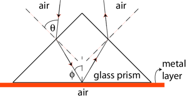
The phenomenon of surface plasmon resonance (SPR) at a planar metal-dielectric interface has been known for a long time [1] and is widely exploited for optical sensing of chemicals [2, 3]. In the Kretschmann configuration, a thin layer of a metal is deposited on one face of a prism made of glass of high refractive index. As shown in Fig. 1, –polarized light shining into the second face of the prism is partially refracted towards the metal layer and then partially reflected out of the third face of the prism. As the angle of incidence of light changes, the reflected light exhibits a sharp dip when the propagation constant along the metal-glass surface closely matches the propagation constant of the surface plasmon wave guided by the metal-air interface. This resonance—which does not occur with –polarized light—occurs due to the real part of the relative permittivity of the metal being negative at optical frequencies. The decreased reflectance indicates high absorption in the metal layer. The width and depth of the resonance is changed when a material is placed below the metal layer. The material can either be the analyte to be sensed or a substrate containing that analyte. The accuracy of the SPR sensor can be enhanced by optimizing the thickness of the metal layer [4].
Surface plasmons can also be localized—on nanoparticles and nanoshells [5] as well as at some locations in certain nanoporous structures [6]. The absorption resonances associated with localized SPs often show up in optical spectrums as narrowband features. Statistical fluctuations of nanoscale morphology can lead to averaging over many different localized resonances, the overall effect being broadened. With this motivation, we decided to investigate the effect on localized SPR (LSPR) of replacing the metal layer in the Kretschmann configuration by a sculptured thin film (STF) of a metal.
The nanostructure of an STF comprises clusters of 3-5 nm diameter. STFs can be made of inorganic or organic dielectrics, metals, and semiconductors, and deposited on variety of substrates, using physical vapor deposition techniques such as thermal evaporation, electron-beam evaporation, and sputtering [7, 8]. STFs are assemblies of naominally parallel and identical nanowires, all of the same shaped. When the nanowires are straight, the STF is called a columnar thin film (CTF). The nanowires are not single grains; thus, CTFs possess inter-columnar porosity as well as intra-columnar porosity, and their nanoscale morphology is appropriate for the simultaneous excitation of multiple LSPRs. Indeed, LSPR has been excited in porous metal thin films due to scattering and therefore without the need for prism coupling, but only in the infrared regime [9]. We demonstrate here, for the first time, the excitation of LSPR using prism coupling on the surface of a porous aluminum thin film in the visible regime.
2 Experiments
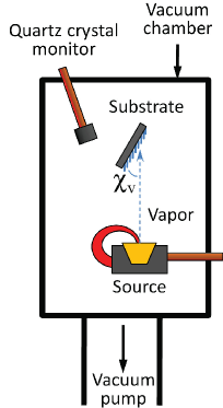
CTFs of aluminum were deposited in an electron-beam evaporation system (PVD-75, KJL Inc.). The oblique-angle-deposition (OAD) technique was used, as depicted schematically in Fig. 2. In an evacuated chamber, with the vacuum base pressure set below Torr, collimated aluminum vapor was directed towards a 2.54-cm 2.54-cm BK7-glass substrate at an angle to the substrate plane. The distance between the aluminum source and the centroid of the substrate was set at cm. The deposition rate was automatically controlled at nm s-1, which was monitored with a resonating quartz crystal sensor. A profilometer (Tencor P-10) was used to measure the metal layer’s average thickness as nm.
The Kretschmann configuration of Fig. 1 was implemented with incident light coming from a 653-nm-wavelength laser diode collimated with a lens and then -polarized after passage through a linear polarizer. The prism was made of BK glass (). The glass substrate on which the aluminum CTF was deposited was separated from the prism by a thin layer of an index–matching fluid. The fraction of the incident power density that exits the right slanted face was measured using an amplifying photodiode. The entire assembly was mounted on an optical table on which the angle can be set to precision.
3 Numerical simulations
The -vs.- relationship was also numerically simulated in the following manner: The –polarization transmittance at the air-glass interface on the left side of the prism was computed as a function of with the Fresnel formula [10], as also the –polarization transmittance at the glass-air interface on the right side of the prism. The -polarization reflectance of glass-CTF-air at the base of the prism was computed as a function of the angle , by using a simple matrix-based formalism wherein we assumed that the columns of the CTF are tilted in the plane of Fig. 1 at an angle with respect to the substrate plane [7]. The effective relative permittivity tensor of the aluminum CTF was obtained from a Bruggeman formalism [11], wherein it was assumed that aluminum is distributed in the form of electrically small prolate spheroids of aspect ratios , the void regions are electrically small spheres, the void regions are vacuous, the porosity , and the relative permittivity of bulk aluminum is . The CTF thickness was taken as nm. The quantity was estimated as the product , while the porosity of the CTF and the incidence angle were varied to fit the experimental data.
4 Results and discussion
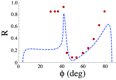
Figure 3 shows measured values of versus for an aluminum CTF. The sudden drop in as increases from to indicates the excitation of an SPR. The wide dip in the – curve is indicative of scattering loss due to the spatial nonuniformity of the distribution of matter in the CTF. Fitting the numerically simulated -vs.- relationship to the experimental data, we found that ; i.e., the CTF is 51.7% volumetrically porous.
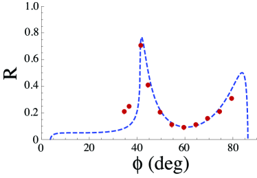
Next, we etched the aluminum CTF using the Transene AL etchant of type A for s. The etching rate at ∘C was 1 nm s-1. The CTF was then rinsed in water and dried by blowing dry nitrogen on it. Thereafter, was measured again for . The measured data is presented in Fig. 4. Clearly, the SPR dip is very different from that in the previous figure. Numerical simulation of the -vs.- relationship suggests that . In other words, etching increased the porosity from 51.7% by 4.3%, and the effect was captured by a widening of the SPR dip.
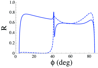
When sub-50-nm thick, CTFs prepared by obliquely directed physical vapor deposition are highly discontinuous, as they are made of nano-islands but with some orientational order which builds up more and more as columns as the thickness increases [13]. As SPR in the Kretschmann configuration had been excited only with dense thin films, the possibility of its excitation using metallic CTFs less than 50 nm thick was questionable. We have now shown both theoretically and experimentally that SPR excitation is possible on sub-50-nm thick aluminum CTFs with porosity %. The SPR dip widens and becomes asymmetric as the porosity increases. As exemplified by Fig. 5, numerical simulations indicate that, as the porosity increases beyond 75%, the SPR dip almost disappears, with a vestigial peak near the onset to the total-internal-reflection regime.
In conclusion, we expect the presented work to eventually lead to peak sensors with high sensitivity because a CTF is a porous material, and SPR excitation would be sensitive to variations in its effective permittivity tensor due to infiltration of its void regions by a fluid [14]. We also hope that this work points to a method to determine the porosity of CTFs, and of more general STFs also.
References
- [1] H. Raether, Surface Plasmons on Smooth and Rough Surfaces and on Gratings, Springer, New York, NY, USA (1983).
- [2] J. Homola, S. S. Yee, and G. Gauglitz, “Surface plasmon resonance sensors: review,” Sens. Actuat. B: Chem. 54, 3-15 (1999) [doi:10.1016/S0925-4005(98)00321-9].
- [3] I. Abdulhalim, M. Zourob, and A. Lakhtakia, “Surface plasmon resonance for biosensing: A mini-review,” Electromagnetics 28, 214-242 (2008) [doi:10.1080/02726340801921650].
- [4] P. Lecaruyer, M. Canva, and J. Rolland, “Metallic film optimization in a surface plasmon resonance biosensor by the extended Rouard method,” Appl. Opt. 46, 2361-2369 (2007) [doi:10.1364/AO.46.002361].
- [5] S. A. Kalele, N. R. Tiwari, S. W. Gosavi, and S. K. Kulkarni, “Plasmon-assisted photonics at the nanoscale,” J. Nanophoton. 1, 012501 (2007) [doi:10.1117/1.2748429].
- [6] A. K. Sarychev and V. M. Shalaev, “Field distribution, Anderson localization, and optical phenomena in random metal-dielectric films,” in: V. A. Markel and T. George (eds.), Optics of Nanostructured Materials, Wiley, New York, NY, USA (2000), pp. 227-282.
- [7] A. Lakhtakia and R. Messier, Sculptured Thin Films: Nanoengineered Morphology and Optics, SPIE Press, Bellingham, WA, USA (2005), Sec. 7.2.
- [8] D. M. Mattox, The Foundations of Vacuum Coating Technology, Noyes Publications, Norwich, NY, USA (2003), pp. 19-24.
- [9] A. I. Maaroof, A. Gentle, G. B. Smith, and M. B. Cortie, “Bulk and surface plasmons in highly nanoporous gold films,” J. Phys. D: Appl. Phys. 40, 5675-5682 (2007) [doi:10.1088/0022-3727/40/18/024].
- [10] M. Born and E. Wolf, Principles of Optics, 6th Ed., Pergamon Press, Oxford, United Kingdom (1980), Sec. 1.5.2.
- [11] J. A. Sherwin, A. Lakhtakia, and I. J. Hodgkinson, “On calibration of a nominal structure-property relationship model for chiral sculptured thin films by axial transmittance measurements,” Opt. Commun. 209, 369-375 (2002).
- [12] www.transene.com/aluminum.html
- [13] R. Messier and J. E. Yehoda, “Geometry of thin-film morphology,” J. Appl. Phys. 58, 3739-3746 (1985) [doi:10.1063/1.335639].
- [14] A. Lakhtakia, “Enhancement of optical activity of chiral sculptured thin films by suitable infiltration of void regions,” Optik 112, 145-148 (2001) [doi:10.1078/0030-4026-00024]; correction: 112, 544 (2001) [doi:10.1078/0030-4026-00088].