Superconducting transition detector in power amplification mode: a tool for cryogenic multiplexing
Abstract
We demonstrate that substantial power gain can be obtained with superconducting transition detectors. We describe the properties of the detector as a power amplifier theoretically. In our first experiments power gain of 23 was reached in a good agreement with the theory. The gain facilitates noise matching of the readout circuit to the detectors in the case of time division multiplexing.
Cryogenic multiplexing is the only practical route towards applications of large format superconducting detector arrays (see, e.g., a review of SQUID multiplexers irwin02 ). Time-division multiplexing (TDM) is one of the basic alternatives. In TDM the outputs from detectors are multiplexed to a single output cable with the help of a cryogenic switch, scanning sequentially through the detectors. Thus each detector is only observed for of the total measurement time. As a consequence, the switching operation multiplies the noise temperature of the post-switch amplifier by , referred to the noise temperature of the pre-switched signals. This makes noise matching of the readout to the low-noise cryodetectors considerably more tedious than without multiplexing.
To keep the readout noise contribution well below that of the detectors, additional power amplification is needed before the switching operation. The gain is normally provided by the readout amplifier, but amplification by the detector is also possible. In this paper, we characterise the achievable power gain, dynamic range, noise and stability of resistively biased transition detectors.
Superconducting transition detectors such as transition edge calorimeters and bolometers mather82 ; richards94 or superconducting wire bolometers luukanen03 are usually operated in voltage biased mode at voltages much below the minimum of the detector curve.irwin95 Such biasing provides high current responsivity, low effective detector Johnson-Nyqvist noise, high stability and good linearity due to the strong negative electrothermal feedback (ETF). However, the detector provides no power gain and the dynamic resistance of the detector is very low (and negative). This calls for a special readout device – the SQUID.
Recently it was demonstrated that the electrothermal feedback of a voltage-biased superconducting bolometer at the curve minimum can be used for efficient noise matching of the detector to standard room temperature readout amplifier in feedback mode penttila06 ; luukanen06 ; helisto07 . This is because the output noise temperature of the transition detector diverges at the minimum helisto07 . Unfortunately this scheme is not well suited to large scale cryomultiplexing due to its limited power gain bandwidth.
In this paper, we analyze the properties of a resistively biased transition detector, operated in the power amplification mode. As an example we use a ’hot-spot’ superconducting wire bolometer luukanen03 , but the results are applicable to other types of thermal detectors also, such as transition-edge sensors kiviranta02 .
Let us consider the circuit shown in Fig. 1 (top left), in which the detector is biased through a bias (or load) impedance instead of using ideal voltage bias. The detector is connected to bath temperature with thermal conductance . The critical temperature of the superconducting detector is and . The bias point resistance of the detector is and is the normal state resistance of the detector. Assuming that the detector is a vacuum-bridge microbolometer wire luukanen03 , its DC properties can be described by simple electrical and thermal equations
| (1) | |||||
| (2) |
where , , , and . A normal-state region, the length of which is determined by the voltage across the detector, , is formed at the center of the bolometer wire. At very low voltages, , the normal phase region shrinks to a hot spot. is the voltage across the detector at the curve minimum. (2) is valid when the transition width is small in comparison to .
We define the power gain as the change of power dissipated in the load resistor versus the change of the input power absorbed by the superconducting transition detector. When the power gain of the detector is
| (3) | |||||
where is the gain of the electrothermal feedback loop and . In (3), describes the thermal time constant of the detector, determined by its heat capacity and thermal conductance.
The DC power gain can be written as
| (4) |
The parameter is the total differential conductance of the circuit from to ground, and . Not suprisingly, the power gain diverges at
| (5) |
where the system becomes unstable at DC. This point corresponds to the voltage over the detector.
The dominant thermal noise mechanisms of the system are well known: the thermal fluctuation noise (phonon noise), Johnson-Nyqvist noise of the detector and Johnson-Nyqvist noise of the bias resistor. The noise power spectral densities are, as referred to the input, respectively,
| (6) | |||||
| (7) | |||||
| (8) |
assuming that the load resistor is at and that the normal phase region of the detector wire is at (the temperature distribution in the hot spot is neglected).
Johnson-Nyqvist noise of the detector can be neglected if . The noise of the load resistance is of the same order as the thermal fluctuation noise: assuming that . Here is a factor taking into account the temperature distribution in the heat link (see mather82 ).
For our intended TDM application, the load resistor would a part of a second thermal circuit (not shown in Fig. 1). Thus a fourth noise mechanism appears: the thermal fluctuation noise of the second circuit. This noise contribution is truly suppressed by the power gain , where is the thermal conductance of the second thermal circuit 111A lower limit on is set by the bias power, dissipated in the load resistor: ..
Power gain reduces the dynamic range of the bolometer compared to the case of strong negative ETF. An estimate of the linear dynamic range is obtained by calculating the change in the output power to second order: and by setting . In the case of ideal voltage bias this gives . When increasing the power gain, the maximum tolerated input power is reduced by a factor . The reduced dynamic range may be a problem in the case of calorimeters, with which maximum dynamic range and linearity is typically required.
The signal bandwidth of the detector is given by (3). In terms of the power gain and the loop gain, the effective time constant becomes . For most applications, such as THz imaging or astrophysics, the thermal bandwidth of superconducting transition detectors is sufficient.
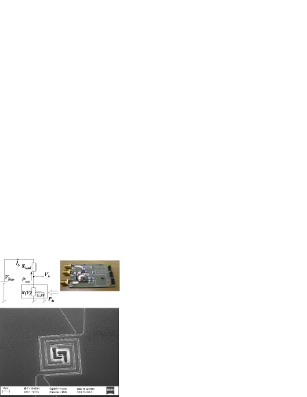
The experimental setup is shown in Fig. 1. The detectors were antenna-coupled superconducting THz bolometers cooled down to K with a pulse-tube cryocooler. The detector element was a piece of NbN film wire with nominal dimensions (length x width x thickness) 24 x 2 x 0.22 m3 and K. To decrease the thermal conductance, the wire is released from the Si substrate by plasma etching helisto07 .
The series connection of the bolometer and was voltage biased with a small bias resistor , not shown in the simplified circuit diagram of Fig. 1. To avoid uncertainties caused by the poorly known THz power coupling, a frequency of 100 MHz was chosen for detector excitation. This frequency is well above the thermal cutoff frequency of the bolometer. The excitation was coupled from the 50 RF source at room temperature to the low temperature stage through a coaxial cable with a transition to microstrip lines on the FR4 chip carrier. Finally, the RF signal was coupled to the bolometer via wire bonds. The source was driving and the bolometer in parallel. The main limitation of power coupling was due the impedance mismatch of the bolometer-load configuration.
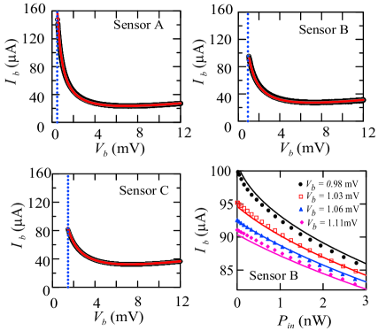
The electrothermal parameters of the bolometers were deduced from curve fits to (see Fig. 2). Three nominally similar devices (Fig. 1 bottom) on a single chip were connected to different load resistances. Typical results were and nW.
From the experimental – curves such as the one shown in Fig. 2 (bottom right), power gain values were obtained as when . The experimental data are in good agreement with the theory (solid curves). The curve with detector voltage nearest to the onset of instability gives a gain of . The resulting gain data as a function of the operating point for the three bolometers are shown in Fig. 3 with the corresponding theoretical curves. Again, a good agreement is found.
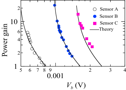
A first look at Eq. (4) suggests that the loop gain should be maximized to maximise the gain. However, with very large and small stable biasing becomes more challenging and the gain becomes more sensitive to small bias voltage variations. Therefore compromises with the load resistance and stability are required. In our experiments, it turned out that the maximum observed power gain depended little on the load resistance value. When using an antenna-coupled device, the detector resistance should be close to the the antenna impedance for best performance.
The bath temperature showed oscillations of about 100 mK due to the pulse tube cryocooler operating cycle. These oscillations, corresponding to 1 % of the saturation power of the detectors, mainly limited our maximum experimental power gain. An interesting limit of validity of the model is reached, when the length of the hot spot becomes of the order of superconducting tunneling length.
We have recently proposed a cryomultiplexing scheme luukanen08 , in which the thermal power gain is exploited. The load resistor is part of a second stage bolometric amplifier/cryoswitch. In this scheme, a power gain of is sufficient to multiplex at least 100 pixels. One possible application is indoors passive THz imaging for detection of concealed weapons. The maximum signal change is the difference between the body and room temperature, about 15 K. Assuming a detection bandwidth of THz, detection efficiency of 20 %, and single mode coupling, this corresponds to power change of pW. Such a power change will not cause a significant nonlinearity at the output of a typical 4 K bolometer at power gain values . The main advantages of utilizing the thermal power gain for cryomultiplexing are process compatibility and low power consumption, when compared with other types of amplifiers, such as SQUIDs irwin02 or cryogenic semiconductors kiviranta06 .
Since our detectors and the setup were not optimized for the power gain experiments, considerably higher power gains should be achievable than are reported here. In conclusion, the power amplification mode of superconducting transition detectors is a feasible tool for a practical, possibly monolithic cryomultiplexer.
We thank Prof. Paul Richards and Mr. Mikko Kiviranta for useful comments and Mr. Leif Grönberg for detector fabrication. The work was partly supported by the European Space Agency, Contract No. 20525/07/NL/CO and by the Academy of Finland (Centre of Excellence in Low Temperature Quantum Phenomena and Devices).
References
- (1) K. D. Irwin, Physica C 368, 203 (2002).
- (2) J. C. Mather, Appl. Opt. 21, 1125 (1982).
- (3) P.L. Richards, J. Appl. Phys. 76, 1 (1994).
- (4) A. Luukanen and J.P. Pekola, Appl. Phys. Lett. 82, 3970 (2003).
- (5) K. D. Irwin, Appl. Phys. Lett. 66, 1998 (1995).
- (6) J. S. Penttilä, H. Sipola, P. Helistö, and H. Seppä, Supercond. Sci. Tech. 19, 319 (2006).
- (7) A. Luukanen, E.N. Grossman, A.J. Miller, P. Helistö, J. S. Penttilä, H. Sipola, and H. Seppä, IEEE Microwave Wireless Comp. Lett. 16, 464 (2006).
- (8) P. Helistö, J.S. Penttilä, H. Sipola, L. Grönberg, F. Maibaum, A. Luukanen, and H. Seppä, IEEE Trans. Appl. Supercond. 17, 310 (2007).
- (9) A. Luukanen, P. Helistö and H. Seppä, ISSTT 2008, 19th Int. Symp. on Space Terahertz Technology, Abstract P5-2 (2008).
- (10) M. Kiviranta, H. Seppä, J. van der Kuur, and P. de Korte, AIP Conf. Proc. 605, 295 (2002).
- (11) M. Kiviranta, Supercond. Sci. Technol. 19, 1297 (2006).