Evidence for Klein tunneling in graphene p-n junctions
Abstract
Transport through potential barriers in graphene is investigated using a set of metallic gates capacitively coupled to graphene to modulate the potential landscape. When a gate-induced potential step is steep enough, disorder becomes less important and the resistance across the step is in quantitative agreement with predictions of Klein tunneling of Dirac fermions up to a small correction. We also perform magnetoresistance measurements at low magnetic fields and compare them to recent predictions.
Graphene is promising for novel applications and fundamental physics due to its remarkable electronic, optical and mechanical properties Neto et al. (2007). At energies relevant to electrical transport, quasi-particles are believed to behave like Dirac fermions with a constant velocity characterizing their dispersion relation . The Klein paradox for massless Dirac fermions predicts that carriers in graphene hitting a potential step at normal incidence transmit with probability one regardless of the height and width of the step Katsnelson et al. (2006). At non-normal incidence, this tunneling problem for 2D massless fermions can be represented as a 1D problem for massive Dirac fermions, with the effective mass proportional to the conserved transverse momentum. The Klein tunneling probability should then depend on the profile of the potential step Katsnelson et al. (2006); Cheianov and Fal’ko (2006); beenakkerreview . Recent experiments have investigated transport across potential steps imposed by a set of electrostatic gates Huard et al. (2007); Williams et al. (2007); Oezyilmaz et al. (2007); Oostinga et al. (2007); Gorbachev_air_bridge ; jeannielau (2007) and results of Ref. Gorbachev_air_bridge support an interpretation of Klein tunneling. We present measurements on six devices which allow a quantitative comparison with Klein tunneling in graphene when the potential profile created by the gates is evaluated realistically Zhang and Fogler (2007). Disorder is sufficiently strong in all our devices to mask effects of multiple reflections between the two steps of a potential barrier, so that all data can be accounted for by considering two independent steps adding ohmically in series. Finally, we probe the transition from clean to disordered transport across a single potential step, and we refine the accuracy of the transition parameter introduced by Fogler et al. fogler_effect_2008 (2008). In a complementary measurement, we show that the effect of a low magnetic field on the Klein tunneling across a potential step in graphene is not explained by existing predictions in the clean limit Levitov .
| Sample | (nm) | (m) | (nm) | () | |
|---|---|---|---|---|---|
| A60 | 60 | 4.3 | 34 | 7.6 | 1800 |
| B100 | 100 | 2.1 | 42 | 3.8 | 1700 |
| B220 | 220 | 2.1 | 42 | 3.5 | 1700 |
| C540 | 540 | 1.74 | 25 | 7.9 | 1400 |
| A860 | 860 | 3.6 | 34 | 7.9 | 1800 |
| C1700 | 1700 | 1.74 | 47 | 1.9 | 1300 |
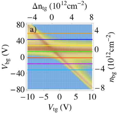
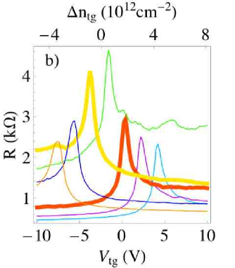
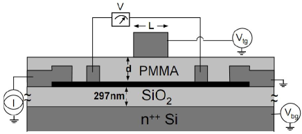
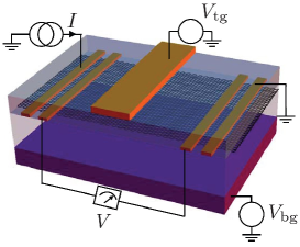
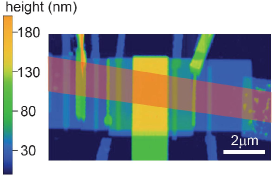
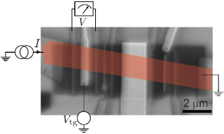
We measure six top-gated graphene devices (typical schematic shown in Fig. 1), whose essential parameters are listed in Table 2. The density far from the top-gated region is set by the back gate according to where is the back gate capacitance per area (from Hall effect measurements on a similar wafer oxidized in the same furnace run), is the electron charge, and is the gate voltage required to attain zero average density Fuhrer1 . The density well inside the top gated region is set by both back gate and top gate voltages according to , where and are the top gate counterparts of and . Throughout this letter we use the notation to identify the contribution of the top gate voltage only, which tunes the potential step height. As described in previous work Huard et al. (2007), an asymmetry with respect to appears in the 4-probe resistance measured across a top-gated region as a function of for fixed back gate voltages (Fig. 2b). This asymmetry quantifies the resistance across the potential step in graphene created by the gates. All graphene top-gated devices were fabricated in the same way, which is described in detail in the Supporting material EPAPS (2008). For electrical characterization, samples are immersed in liquid Helium at 4 K and four-terminal measurements are made using a lock-in amplifier at a frequency 32 Hz with a bias current of 100 nA. All samples show typical monolayer graphene spectra measured by Raman spectroscopy and exhibit the quantum Hall plateaus characteristic of graphene when measured in perpendicular magnetic fields up to 8 T at 4 K (see Supporting material EPAPS (2008)).
In order to extract the resistance of the p-n interfaces only, we measure the odd part of resistance about Huard et al. (2007):
| (1) |
where is the four-terminal resistance as a function of the densities far from the top gated region and well inside that region. Extracting the odd part from the measured resistance requires an accurate determination of the densities and . This is made by the measurement of three independent quantities , , and . We carefully measure these quantities by using the quantum Hall measurements at 8 T and electron-hole symmetryEPAPS (2008). There are two physical interpretations for depending on the relative magnitude of two length scales: the mean free path (well defined for or equivalently for a conductivity ) and the top gate length . For , after crossing the first interface of the barrier carriers lose all momentum information before impinging on the second interface. In this case, the total barrier resistance can be modeled by two junctions in series. The expression where () denotes the theoretical value of the resistance of a single p-n ( p-p) interface, can then be compared directly to the experimental quantity Huard et al. (2007). For , multiple reflections occur between the two interfaces of the barrier, which is predicted to reduce the total barrier resistance EPAPS (2008).
As all devices have modest mobility, we start by using a diffusive model to calculate and . In this model, due to disorder the resistance depends on the local resistivity (measured for a uniform density at ) at each position :
| (2) |
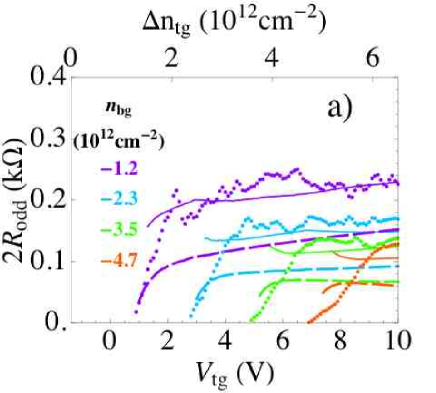
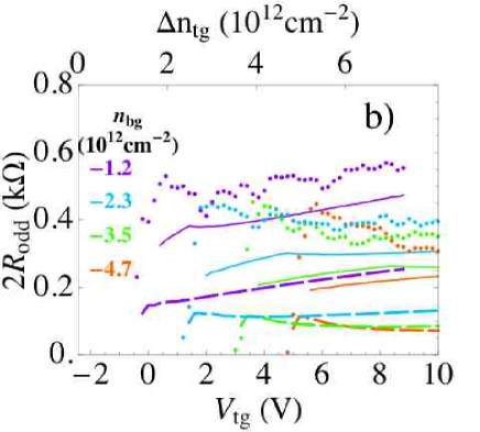
Figure 3 compares the experimental curves for as a function of at several for samples A60 and C540 to the corresponding predictions. Clearly, the diffusive model represented by the dashed lines predicts resistance values considerably below the experimental curves, hinting that transport through the device cannot be viewed as entirely diffusive. Following the calculation by Fogler et al. fogler_effect_2008 (2008), we retain the diffusive model for the region away from the interface, but replace it by a ballistic interface model for a region extending one mean free path in either direction from the location where density changes polarity footnote_xbal_le (2008). Thus,
| (3) |
where the two last terms are taken from Eq. 2, but with the integral excluding . The first two terms are the ballistic contributions to the interface resistance for bipolar and monopolar configurations, and can be calculated individually as follows. All conduction channels on the low-density side of a monopolar junction should have transmission nearly 1 through the junction Cayssol (2008), so . The bipolar case was addressed by Zhang and Fogler Zhang and Fogler (2007):
| (4) |
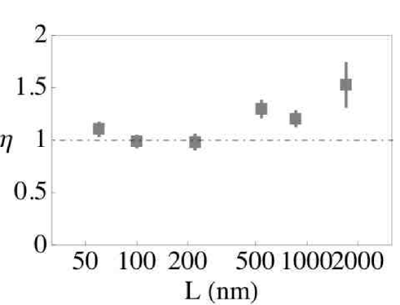
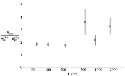
where is Planck’s constant, is the dimensionless strength of Coulomb interactions ( is the average dielectric constant of SiO2 and cross-linked PMMA measured at 4K), and is the slope of the density profile at the position where the density crosses zero (density profile calculated from the classical Poisson equation with realistic gate geometry, temporarily treating graphene as a perfect conductor). Expression 4 refines this calculation to take into account non-linear screening of graphene close to zero density, going beyond the linear model used in Ref. Cheianov and Fal’ko (2006). The prefactor in Eq. (4) is determined numerically Zhang and Fogler (2007). In our case, and the prefactor is predicted to be EPAPS (2008). In order to test this prediction will be used as a single fit parameter across all samples and densities. The solid lines in Fig 3 were generated by Eq. 3, choosing to best account for all experimental curves in all devices (voltages give a similar agreement, not shown for clarity). The slight discrepancy between theoretical and experimental values of might be due in part to exchange and correlation effects. Trying to fit the data using a naive linear potential model requires an independent fitting parameter for each device, and even with the best fit to the data, some qualitative trends of the experimental data cannot be accounted for by this model, as described in detail in the Supporting material EPAPS (2008). This mismatch between the linear model and the data indicates the importance of accounting for non-linear screening close to zero average density. We continue by calculating the ratio , for all devices, for all measured and , using Eq. 3. The histogram of is sharply peaked at a certain value with a small peak width EPAPS (2008). For all devices except C1700, regardless of their length , is close or slightly higher than 1 when using (Fig. 4), which indicates that the resistances of both interfaces of the potential barrier simply add in series, and a single p-n junction is less sensitive to disorder than transport between the two interfaces of a potential barrier. Fogler et al. introduced the parameter to describe the clean/disordered transition in a single p-n junction, where is related to the mobility by fogler_effect_2008 (2008). According to Ref. fogler_effect_2008 (2008), when the ballistic contribution in Eq. (3) dominates and the junction is in the clean limit, whereas for , the diffusive contribution in Eq. (3) dominates and the junction is in the disordered limit. The threshold marks the transition where ballistic contribution must be taken into account since it is comparable to the diffusive contribution. In the following, we refine this transition threshold experimentally. From Fig. 4 and Table 1, it seems that transport is indeed well described by Eq. (3) when but more poorly for C1700 where , where we find that is further than 1 and has a large spread of values. In addition, Fogler et al. predict that the diffusive contribution to the the interface resistance will be negligible for , which is reached in several of our devices for densities . At these densities, in spite of our devices’ modest mobility, the junction can be considered as disorder-free since the calculated ballistic contribution to is 10 times higher than the diffusive one, which allows us to make a rather accurate measurement of the ballistic contribution alone in this clean limit, and match it well with the ballistic terms in Eq. (3).
In a recent experiment where suspended top gates were used, for one sample the agreement with Eq. 2 – the disordered limit – was very good (sample S3 in Ref. [9]). This is due to a much larger distance between the top gate and the graphene sheet, and much smaller density range than in the present work, likely due to lower dielectric constant combined with mechanical instability of the top gate when applying higher voltages. These two factors considerably reduce (around 80 times), which is not fully balanced by the cleaner graphene of Ref. Gorbachev_air_bridge ( 2-5 times smaller). We estimate for device S3 reported in Ref. Gorbachev_air_bridge . Note that two other devices on substantially cleaner graphene (S1 and S2 in Ref. Gorbachev_air_bridge ) support an interpretation of Klein tunneling with and respectively. From the present work and from the result of Ref. Gorbachev_air_bridge , one can see that the transition between clean and disordered transport in p-n junctions seems to be sharp: for the clean limit applies, for the disordered limit applies and in between neither limit is valid. footnote_fluc (2008).
Being sharply dependent on angle of incidence, transport through potential steps in graphene should be sensitive to the presence of a magnetic field, which bends electron trajectories. For the predicted interface conductance in the clean limit is
| (5) |
where is the conductance at zero field, and is the distance over which the potential rises, which is proportional to the thickness of the oxide Levitov . We measure as a function of magnetic field in two devices C540 and C1700 on the same graphene sheet but with different top gate dielectric thickness (Table 1). We use the experimental and the best parameter to fit all curves within the same device (see Supporting material). The parameters for C540 and C1700 are found to be 65 nm and 55 nm respectively, whereas C1700 has the thicker dielectric (see Table 2). Further theoretical work is needed to explain this discrepancy.
In conclusion, we show evidence for Klein tunneling across potential steps in graphene with a quantitative agreement to a model with one free parameter describing screening properties in graphene. The crossover between clean and disordered regimes occurs as a function of the parameter around 1 as predicted by Fogler et al. fogler_effect_2008 (2008). More work is needed to go into the fully ballistic regime, and also to measure directly the angle dependence of Klein tunneling Cheianov and Fal’ko (2006).
We thank J. A. Sulpizio for help with fabrication and characterization, and M. Fogler, D. Novikov, L. Levitov, and A. Young for enlightening discussions. We also thank A. Savchenko for pointing out the need to take into account the resistance of the monopolar junction in the predictions for . While this work was under review, we became aware of related work by A. Young et al., in which evidence is seen for ballistic transport across a full npn junction Young (2008). This work was supported by the MARCO/FENA program and the Office of Naval Research contract N00014-02-1-0986. N. Stander was supported by a William R. and Sara Hart Kimball Stanford Graduate Grant. Work was performed in part at the Stanford Nanofabrication Facility of NNIN supported by the National Science Foundation under Grant ECS-9731293. Critical equipment (SEM,AFM) was obtained partly on Air Force Grants FA9550-04-1-0384 and F49620-03-1-0256.
Supplementary material
sectionGraphene characterization
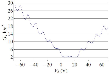
We measure 2-probe conductance in each sample at high magnetic field (8 T), in order to verify it has the unique behavior of a single sheet. For example Fig. 5 shows conductance measured in sample C540 at 8 T (note that an estimated contact resistance has been taken into account ). The plateaus in are at values , …, characteristic of a single layer. Appearance of peaks between plateaus was predicted by Abanin and Levitov, for a 2-probe measurement. abaninlevitov .
I Extracting the odd part of the resistance
Extracting the odd part of the resistance requires the determination of three quantities: The ratio between the top gate capacitance and the back gate capacitance , , which corresponds to zero average density far from the top gated region,and which corresponds to zero average density below the top gated region, when . A good approximation to these parameters can be extracted from Fig. 1a of the paper, since the voltage offsets are the coordinates of the global maximum in resistance and the slope of the diagonal peaked line gives the ratio . However, the odd part turns out to be particularly sensitive to , so that a mere estimation of the peak position is not enough.
Instead, we measure the resistance for each device as a function of voltages and at 8 T in the Quantum Hall regime. The position of the transition between the first and second conductance plateaus in for each value of leads to a determination of the ratio within . The determination of the voltages and can be done accurately by symmetrizing the resistance in Fig. 1 of the paper with respect to the point :
| (6) |
and choosing the point which leaves this resistance the most unchanged.
| Sample | L (nm) | w (m) | d (nm) | (V) | (V) | (nF.cm-2) | (cm2V-1s-1) | |
|---|---|---|---|---|---|---|---|---|
| A60 | 60 | 4.3 | 34 | 25.65 | -1.36 | 92 | 1800 | 7.6 |
| B100 | 100 | 2.1 | 42 | 9.35 | -0.49 | 69 | 1700 | 3.8 |
| B220 | 220 | 2.1 | 42 | 10.95 | -0.73 | 69 | 1700 | 3.5 |
| C540 | 540 | 1.74 | 25 | 18.65 | -2.42 | 107 | 1400 | 7.9 |
| A860 | 860 | 3.6 | 34 | 25.5 | -2.35 | 92 | 1800 | 7.9 |
| C1700 | 1700 | 1.74 | 47 | 13.4 | -1.35 | 52 | 1300 | 1.9 |
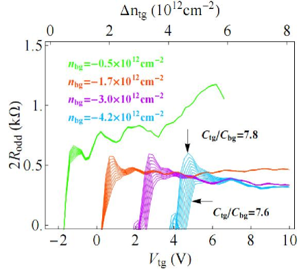
Still, the uncertainty of on the capacitance ratio leads to some uncertainty on the odd part of the resistance. However, this uncertainty remains negligible except at low densities (see Fig. 7).
II Comparing the experimental value to theoretical models of the junction interface resistance
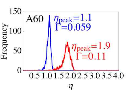
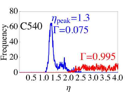
Figures 3a and 3b in the paper show the experimental in comparison to the theoretical , for the two devices A60 and C540 at several within both clean and disordered models. In order to quantify the compatibility of the theory to the experiment, we define as the ratio . We determine the ratio for all measured densities and calculate the corresponding histogram for using two models of transmission across a single potential step in graphene: diffusive and ballistic. corresponds to perfect agreement between theory and experiment in the limit where (see paper). Figures 8a and Figs. 8b show two histograms of each, for devices A60 and C540, respectively. The red histogram is using a diffusive model while the blue one is using a ballistic model. We follow the same procedure for all devices, and extract the value associated with the the diffusive theory and ballistic theory, at the center of the peaked histogram together with its width () , by fitting the data to the following Lorentzian:
| (7) |
In the paper, Fig. 4 presents and small error bars for when using the ballistic model with a fitting parameter . This is complemented here by Fig. 9 showing the wide spread of for some devices, along with a much lower predicted value of when using the diffusive model. Note that B100 and B220 have a relatively smaller spread in when using the diffusive model, which is due to a smaller range of densities. In contrast the relatively small spread of when using the diffusive theory for A60 is not due to a smaller range of densities nor due to the short dimension of the top gate. We currently do not understand this feature, although the spread is still larger than the spread in when using the ballistic model.
III Multiple reflections between interfaces of a potential barrier
One of the goals of the main paper was to investigate the transition from diffusive to ballistic transport through the potential barrier by making the top gate length smaller than the mean free path of the carriers. In this limit the transport across the whole potential barrier is expected to be ballistic (no disorder), and charge carriers are subject to multiple reflections on the two interfaces of the barrier.
III.1 Without phase coherence
The transmission probability across the whole potential barrier is related to the transmission probability across a single interface by:
| (8) |
Hence,
| (9) |
Therefore the total conductance for a width is given by
| (10) |
where is the component of the wavevector along the potential interface. One can compare this to the conductance across a single interface
| (11) |
so that
| (12) |
According to Ref. Cheianov and Fal’ko (2006), with therefore,
| (13) |
Using the notations of our paper, this translates into a resistance
| (14) |
Therefore, for a length small enough (), the odd part of the resistance should be such that
| (15) |
As seen from Fig. 4 in the paper, this regime is never achieved fully in the experiments but may be the cause of the smaller for the shortest top gate.
III.2 Including phase coherence
In the phase coherent regime, the above derivation remains valid up to a phase term in the transmission:
| (16) |
where is the time spent between back and forth bounces and is the angle of incidence. This simplifies into
| (17) |
with the density below the top gate. Phase coherent length in our devices is of the order of a few microns, extracted from a similar device in Ref. Huard et al. (2007)
IV n-p junctions in finite magnetic field
As explained in the paper transport through potential steps in graphene should be sensitive to the presence of a magnetic field, which bends electron trajectories. For instance, in the clean limit the angle at which carriers are transmitted perfectly should be given by where and is the distance over which the potential rises, which is proportional to the thickness of the oxide Levitov . For the predicted interface conductance is
| (18) |
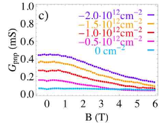
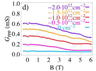
where is the conductance at zero field. Since Eq. (18) is a prediction for the conductance of a single p-n interface and in both devices, can be interpreted as the conductance of a single p-n interface (canceling out the monopolar bulk magnetoresistance, whose source in not well understood). For several gate voltages such that , we measure as a function of magnetic field (Fig. 10) in two devices C540 and C1700 on the same graphene sheet but with different top gate dielectric thickness (Table 1). We use the experimental and the best parameter to fit all curves within the same device. The parameters for C540 and C1700 are found to be 65 nm and 55 nm respectively, whereas C1700 has the thicker dielectric (see Table 2).
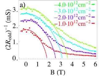
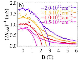
We also show here how to extract the n-p interface conductance in the presence of magnetic field. Both C540 and C1700 satisfy the condition (Fig. 4 of our paper), thus the barrier resistance can be viewed as that of two n-p interfaces in series. In this case , where () is the resistance of the barrier when (). Figures 11a-d show and for C540 and C1700, as a function of magnetic field, at several . The flatness of the curve is a measure of how well and were determined. Also, at all measured densities, in both devices, which is consistent with the zero magnetic field case. Finally, we note a weak localization dip in both devices C540 and C1700 in the conductance near for all densities.
![[Uncaptioned image]](/html/0806.2319/assets/x17.png)
![[Uncaptioned image]](/html/0806.2319/assets/x18.png)
IV.1 Fabrication details
The substrate used in these experiments is a highly n-doped Si wafer with a nominal resistivity of less than . Standard wafers experience carrier freeze-out and hence hysteretic response to applied gate voltage at temperatures below .
All graphene sheets were produced by successive mechanical exfoliation of Highly Oriented Pyrolytic Graphite grade ZYA from General Electric (distributed by SPI) using an adhesive tape (3M Scotch Multitask tape with gloss finish), then deposited onto a layer of SiO2 297 nm thick grown by dry oxidation at on a highly n-doped Si substrate, which serves as a global back gate. Before deposition of graphene, the substrate was cleaned by Piranha etch. After suitable sheets were located with respect to alignment marks by optical microscopy, metallic probes were patterned using standard electron beam lithography followed by electron beam evaporation of Ti/Au (5 nm/25 nm thick). Afterward, the graphene sheets were etched in dry oxygen plasma (1:9 O2:Ar) into the desired shape, and one or two layers of Polymethyl Methacrylate (PMMA, molecular mass 950K or 495K at 2% in anisole) were spun on top of it, then cross-linked using electron beam with a dose of . In a final e-beam lithography step, the top gates were patterned on top of the cross-linked layer, followed by electron beam evaporation of Ti/Au ( nm/ nm-55 nm thick).
References
- Neto et al. (2007) A. H. Castro Neto, F. Guinea, N. M. R. Peres, K. S. Novoselov, and A. K. Geim, Rev. Mod. Phys. (to be published).
- Katsnelson et al. (2006) M. I. Katsnelson, K. S. Novoselov, and A. K. Geim, Nat. Phys. 2, 620 (2006).
- Cheianov and Fal’ko (2006) V. V. Cheianov and V. I. Fal’ko, Phys. Rev. B 74, 041403 (2006).
- (4) C. Beenakker, cond-mat/0710.3848
- Huard et al. (2007) B. Huard, J. A. Sulpizio, N. Stander, K. Todd, B. Yang, and D. Goldhaber-Gordon, Phys. Rev. Lett. 98, 236803 (2007).
- Williams et al. (2007) J. R. Williams, L. DiCarlo, C. M. Marcus, Science 317, 638 (2007).
- Oezyilmaz et al. (2007) B. Özyilmaz, P. Jarillo-Herrero, D. Efetov, D. A. Abanin, L. S. Levitov, P. Kim, Phys. Rev. Lett 99, 166804 (2007).
- Oostinga et al. (2007) Jeroen B. Oostinga, Hubert B. Heersche, Xinglan Liu, Alberto F. Morpurgo, Lieven M. K. Vandersypen, Nature Materials 7, 151 (2008).
- (9) R. V. Gorbachev et al., cond-mat/0804.2081 (2008).
- jeannielau (2007) Gang Liu, Jairo Valesco Jr, Wenzhong Bao, Chun Ning Lau, Appl. Phys. Lett. 92, 203103 (2008).
- Zhang and Fogler (2007) L. M. Zhang and M. M. Fogler, Phys. Rev. Lett. 100, 116804 (2008).
- fogler_effect_2008 (2008) M. M. Fogler, D. S. Novikov, L. I. Glazman, and B. I. Shklovskii, Phys. Rev. B 77, 075420 (2008).
- footnote_xbal_le (2008) The mean free path is a function of carrier density, and hence it varies as one approaches the interface. Which value of mean free path is appropriate to characterize the region near the interface over which transport is ballistic? Following Fogler et al. fogler_effect_2008 (2008) we self-consistently define a distance over which transport near the interface is ballistic: , where the interface is at , is derived from solution of the classical Laplace equation for the actual device geometry, and .
- (14) A. V. Shytov, Nan Gu, and L. S. Levitov cond-mat/0708.308 (2008).
- (15) J. H. Chen, C. Jang, M. S. Fuhrer, E. D. Williams, M. Ishigami, Nature Physics 4, 377 (2008).
- EPAPS (2008) See Supporting material online EPAPS.
- Cayssol (2008) J. Cayssol et al. cond-mat/0810.4568 (2008).
- EPAPS (2008) M. M. Fogler, private communication.
- footnote_fluc (2008) Near , where density fluctuations are bigger than , disorder should dominate fogler_effect_2008 (2008).
- Young (2008) A. Young et al., Nature Physics, in press.
- (21) D. Abanin and L. Levitov, cond-mat/0804.4043
- (22) A. C. Ferrari, J. C. Meyer, V. Scardaci, C. Casiraghi, M. Lazzeri, F. Mauri, S. Piscanec, D. Jiang, K. S. Novoselov, S. Roth and A. K. Geim, Phys. Rev. Lett. 97,187401 (2006).