Remote hole-doping of Mott insulators on the nanometer scale
Abstract
At interfaces between polar and nonpolar perovskite oxides, an unusual electron-doping has been previously observed, due to electronic reconstructions. We report on remote hole-doping at an interface composed of only polar layers, revealed by high-resolution hard x-ray core-level photoemission spectroscopy. In LaAlO3/LaVO3/LaAlO3 trilayers, the vanadium valence systematically evolves from the bulk value of V3+ to higher oxidation states with decreasing LaAlO3 cap layer thickness. These results provide a synthetic approach to hole-doping transition metal oxide heterointerfaces without invoking a polar discontinuity.
pacs:
79.60.Jv, 71.27.+a, 73.20.-r, 78.67.PtWhen assembled with atomic precision, the interface between polar and nonpolar perovskite oxides can be engineered to undergo new classes of interface electronic reconstructions, energetically driven by electrostatic boundary conditions HesperK3C60 . At such a polar discontinuity between two insulators, metallic, magnetic, and superconducting states have recently been discovered OhtomoLTOSTO ; OkamotoLSTO ; OhtomoLAOSTO ; NakagawaLAOSTO ; HuijbenLAOSTO ; ThielLAOSTO ; BrinkmanLAOSTO ; Pentcheva-calc ; Lee-calc ; ReyrenLAOSTO . For example, multilayers consisting of a band insulator SrTiO3 and a Mott insulator LaTiO3 exhibit metallic conductivity OhtomoLTOSTO ; OkamotoLSTO ; Pentcheva-calc ; shibuya ; TakizawaLTOSTO . Interfaces between two band insulators, LaAlO3 and SrTiO3, also show metallic conductivity, and furthermore show a remarkable termination layer dependence OhtomoLAOSTO . That is, the (LaO)+/(TiO2)0 interfaces (“-type” interfaces) are metallic, while the (AlO2)-/(SrO)0 interfaces (“-type” interfaces) remain insulating. In order to interpret such properties, “electronic reconstructions” to avoid the “polar catastrophe” have been proposed HesperK3C60 ; NakagawaLAOSTO ; Lee-calc ; polarReview . For the (001) plane of LaAlO3, where (LaO)+ and (AlO2)- are alternately stacked, in order to avoid the divergence of electrostatic potential with the number of layers, some charge redistribution must occur. For the (LaO)+/(TiO2)0 interface, the divergence can be avoided if half an electron (e/2) is added to the interfacial region through the change of the Ti valence from Ti4+ to Ti3.5+. Moreover, the metallic transport at the LaAlO3/SrTiO3 interfaces has been found to occur beyond a critical LaAlO3 layer thickness of - 6 unit cells (uc) ( - 2.3 nm) HuijbenLAOSTO ; ThielLAOSTO .
This electronic reconstruction scenario should, in principle, be symmetric between electrons and holes. Despite significant effort, however, no examples of hole-doping have been experimentally demonstrated to date. The insulating -type LaAlO3/SrTiO3 interface was found to be compensated by oxygen vacancies, rather than inducing holes NakagawaLAOSTO . KTaO3 grown on the TiO2-terminated surface of SrTiO3, also motivated to induce hole-doping, was found experimentally to have -type carriers, likely originating from kinetically induced oxygen vacancies in the SrTiO3 substrate KalabukhovKTO . These negative results likely reflect the lack of energetically accessible higher oxidation states (such as Ti5+) at these interfaces, and suggest that an interface must by suitably engineered to induce hole-doping. Furthermore, in the absence of demonstrable hole-doping, questions have been raised on the applicability of an electronic reconstruction picture as the origin of the electrons at the LaAlO3/SrTiO3 interface KalabukhovLAOSTO ; SeimonsLAOSTO ; HerranzLAOSTO .
Recently, LaAlO3/LaVO3 multilayers, which are composed of only polar planes, have been fabricated and studied by photoemission spectroscopy (PES) HottaLVO_PES ; WadatiLVO . It was found that the V core-level spectra had not only V3+ components as expected from the chemical composition, but also a higher oxidation state V4+ component. Whether this V4+ component originated simply from chemical imperfections or some electronic reconstruction mechanism was unclear. In this work, we have performed a systematic LaAlO3 cap layer thickness dependence of the V valence in LaAlO3/LaVO3/LaAlO3 trilayers using hard x-ray PES to probe deeply buried structures. The evolution of the vanadium valence with cap layer thickness demonstrates that heterointerfaces composed of only polar layers, free of any ionic polar discontinuity, can be remotely hole-doped depending on proximity to a polar surface.
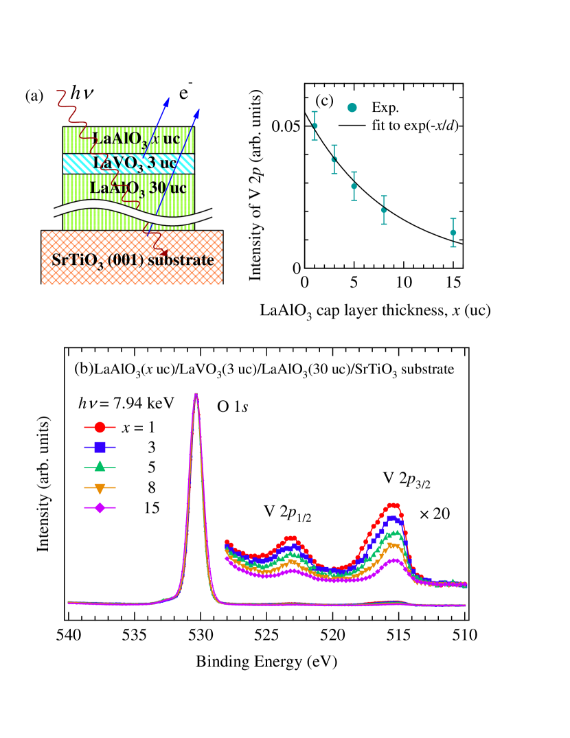
LaAlO3( uc)/LaVO3(3 uc)/LaAlO3(30 uc) trilayers, with varying LaAlO3 cap layer thickness , were grown on the atomically flat, TiO2-terminated (001) surface of SrTiO3 substrates using pulsed laser deposition (PLD), as schematically shown in Fig. 1 (a). All the trilayers were confirmed to be fully strained to the substrate by off-axis x-ray diffraction. The structures were grown at 600 ∘C under an oxygen partial pressure of Torr, with a laser fluence of J/cm2, following the previous optimization for two dimensional layer-by-layer growth of LaVO3 HottaLVO . Hard x-ray PES measurements were performed at the undulator beamline BL29XU of SPring-8, using a hemispherical electron energy analyzer, SCIENTA R4000-10kV. Details of the apparatus including x-ray optics are described elsewhere TakataHXPES ; TamasakuHX ; IshikawaHX . Samples were transferred from the PLD chamber to the spectrometer chamber ex situ and no surface treatment was performed prior to PES measurements. All the measurements were carried out at room temperature, and the total energy resolution was set to about 200 meV. The Fermi level () position was determined using gold spectra.
Figure 1 (b) shows the O and V core-level spectra of the LaAlO3/LaVO3/LaAlO3 trilayers with varying LaAlO3 overlayer thickness , normalized to the O peak height. Because the LaVO3 layer was only 3 uc thick, the V core level signals were very small compared with those of O . Figure 1 (c) shows the integrated intensity of the V core level as a function of LaAlO3 cap layer thickness . With increasing , the intensity of the V core level decreased, and the intensities were well fit by the exponential decay with uc ( nm).
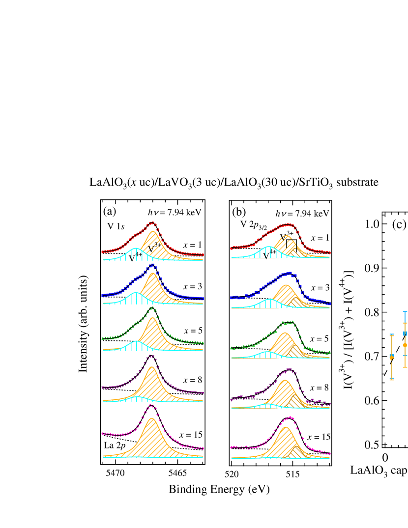
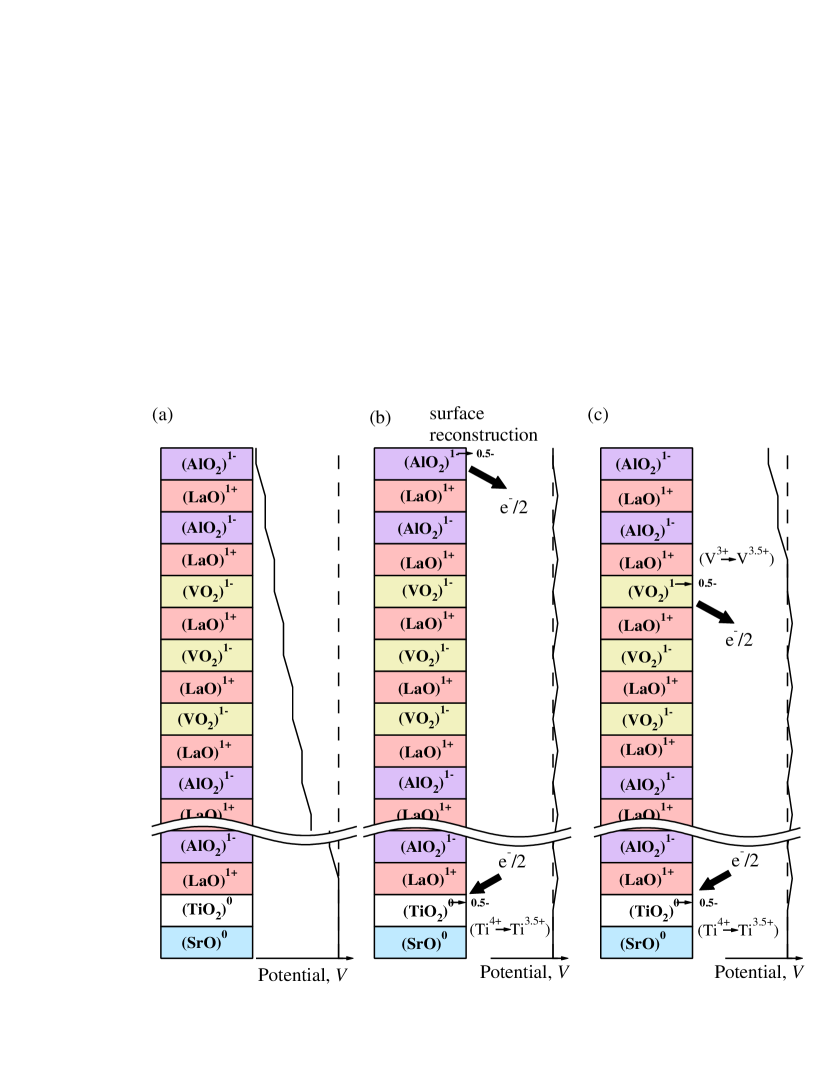
Figure 2 (a) and (b) shows the V and V core-level spectra of the LaAlO3/LaVO3/LaAlO3 trilayers and their line-shape decomposition. In both spectra, one can clearly see two components. The low and high binding energy components can be assigned to V3+ and V4+, respectively LCVO . The V and V core-level spectra have been decomposed into two features by line-shape analysis. With increasing LaAlO3 cap layer thickness, the structure on the higher binding-energy side (due to V4+) decreases, meaning that as the LaVO3 layer is more deeply buried in the LaAlO3 environment, the V ion recovers the V3+ character of bulk LaVO3. In the line-shape analysis of the V core-level spectra, an additional component from the La core level located around eV WadatiLVO has also been taken into account [Fig. 2 (a)]. For the line-shape analysis of the V core-level spectra, three components were needed to reproduce the experimental results well. One feature located around eV is the V4+ component. Two other features located around eV and eV represent the multiplet structure of the V3+ component [Fig. 2 (b)], as confirmed by cluster-model calculations including atomic multiplet structure. Figure 2 (c) shows the resulting V3+ relative intensity as a function of LaAlO3 cap layer thickness. With increasing thickness, the V3+ component increases and saturates toward beyond uc.
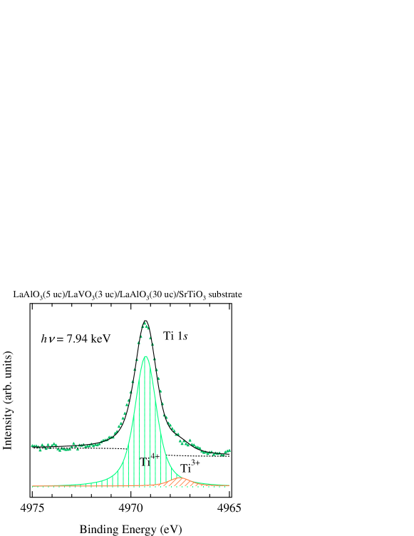
Let us discuss the origin of the present observations, together with the previous report that the valence distribution of V was highly asymmetric in the LaVO3 layers in LaAlO3/LaVO3/LaAlO3 HottaLVO_PES ; WadatiLVO . That is, V4+ was preferentially distributed on the top side of the LaVO3 layers. These features can be explained by considering the electrostatic potential of the trilayer, as schematically shown in Fig. 3. If all of the constituent materials preserve their bulk electronic and atomic configurations, the LaAlO3/LaVO3/LaAlO3 trilayers films would consist of only polar planes and suffer from the “polar catastrophe” as shown in Fig. 3 (a). In order to avoid this, two types of reconstructions that dramatically alter the electrostatic potential may be possible. In the first scenario [Fig. 3 (b)], the polar (AlO2)- surface of LaAlO3 is reconstructed LAOsurf1 ; LAOsurf2 , resulting in the net ejection of the charge e/2. Therefore, the LaVO3 layer is not affected. In the second scenario [Fig. 3 (c)], the valence of the V ion changes from V3+ to V3.5+ and thereby e/2 is removed from the top side of the embedded LaVO3 layer. In either case, e/2 is effectively transferred to the SrTiO3 substrate. This can be seen in Fig. 4, showing typical Ti core-level spectra from the film-substrate interface of the LaAlO3/LaVO3/LaAlO3 trilayers. Despite the 38 uc thickness of the trilayer, Ti signals from the SrTiO3 substrate were clearly observed due to the long electron escape depth using hard x-ray PES.
Between these two scenarios, the energetically more favorable process will be realized for a given LaAlO3 cap layer thickness. These two scenarios can be considered as two competing processes: In order to prevent the “polar catastrophe”, some charge redistribution must occur, resulting in the removal of e/2 from the top layer and transferred to the bottom of the polar mulilayers NakagawaLAOSTO . When the LaAlO3 cap layer thickness is thin, the electrostatic potential within the LaAlO3 cap layer remains small and the valence change of V (V3+ V4+) occurs [Fig. 3 (c)]. On the other hand, as the LaAlO3 cap layers become thicker, the potential within the top LaAlO3 cap layers grows in proportion to the LaAlO3 cap layer thickness, and this increasing energy cost cannot be compensated simply by the valence change of V. Therefore, the reconstruction of the LaAlO3 surface would suppress the potential divergence of the entire trilayer more effectively and the valence change of V becomes unnecessary – indeed, energetically unfavorable. Thus, the valence state of V in the LaVO3 layers returns to its original bulk-like value of V3+ [Fig. 3 (b)].
It is worth remarking on the relationship between the present observations and the thickness dependence of the interface carrier density in LaAlO3/SrTiO3 heterostructures, showing a critical LaAlO3 layer thickness of 4 - 6 uc HuijbenLAOSTO ; ThielLAOSTO . This behavior may also be interpreted in the same scenario: For thin LaAlO3 layer thickness, the electrostatic potential within the LaAlO3 layer remains small, and therefore the redistribution of charge does not have to occur, resulting in few carriers induced at the LaAlO3/SrTiO3 interface. With increasing LaAlO3 thickness, reconstruction of the LaAlO3 surface donates e/2 to the interfacial region, inducing carriers on the SrTiO3 side. Whereas the LaAlO3/SrTiO3 structures induce electrons at the interface, by designing polar LaAlO3/LaVO3/LaAlO3 trilayers, we have demonstrated remote hole-doping into a Mott insulator. This technique should be quite general, so long as electronic reconstructions are energetically favorable to surface reconstructions on short length scales. These results, together with previous studies of LaAlO3/SrTiO3 polar discontinuities, demonstrate the design of both positive and negative remote charge injection at heterointerfaces, opening a new door to the materials science and engineering of transition metal oxides.
In conclusion, we have performed a hard x-ray photoemission spectroscopy study on LaAlO3/LaVO3/LaAlO3 trilayers. The V core-level spectra showed two components, which we assigned to V3+ and V4+ valence states. The intensity of the V3+ component increased with LaAlO3 cap layer thickness and saturated beyond unit cells. This behavior can be explained by competing electronic reconstructions. This work demonstrates the ability to artificially hole-dope oxide heterostructures by atomic control of the electrostatic boundary conditions.
We thank D. A. Muller and G. A. Sawatzky for fruitful discussions. This work was supported by a Grant-in-Aid for Scientific Research (A19204037) from the Japan Society for the Promotion of Science and a Grant-in-Aid for Scientific Research in Priority Areas “Invention of Anomalous Quantum Materials” from the Ministry of Education, Culture, Sports, Science and Technology. MT acknowledges support from the Japan Society for the Promotion of Science for Young Scientists.
References
- (1) R. Hesper, L. H. Tjeng, A. Heeres, and G. A. Sawatzky, Phys. Rev. B 62, 16046 (2000).
- (2) A. Ohtomo, D. A. Muller, J. L. Grazul, and H. Y. Hwang, Nature 419, 328 (2002).
- (3) S. Okamoto and A. J. Millis, Nature 428, 630 (2004).
- (4) A. Ohtomo and H. Y. Hwang, Nature 427, 423 (2004).
- (5) N. Nakagawa, H. Y. Hwang, and D. A. Muller, Nature Mater. 5, 204 (2006).
- (6) M. Huijben, G. Rijnders, D. A. Muller, S. Bals, S. Van Aert, J. Verbeeck, G. Van Tendeloo, A. Brinkman, and H. Hilgenkamp, Nature Mater. 5, 556 (2006).
- (7) S. Thiel, G. Hammeri, A. Schmehl, C. W. Schneider, and J. Mannhart, Science 313, 1942 (2006).
- (8) A. Brinkman, M. Huijben, M. Van Zalk, J. Huijben, U. Zeiter, J. C. Maan, W. G. Van der Wiel, G. Rijnders, D. H. A. Blank, and H. Hilgenkamp, 6, 493 (2007).
- (9) R. Pentcheva and W. E. Pickett, Phys. Rev. Lett. 99, 016802 (2007).
- (10) W.-C. Lee and A. H. MacDonald, Phys. Rev. B 76, 075339 (2007).
- (11) N. Reyren, S. Thiel, A. D. Caviglia, L. Fitting Kourkoutis, G. Hammert, C. Richter, C. W. Schneider, T. Kopp, A.-S. Rüetschi, D. Jaccard, M. Gabay, D. A. Muller, J.-M. Triscone, and J. Mannhart, Science 317, 1196 (2007).
- (12) K. Shibuya, T. Ohnishi, M. Kawasaki, H. Koinuma, and M. Lippmaa, Jpn. J. Appl. Phys. 43, L1178 (2004).
- (13) M. Takizawa, H. Wadati, K. Tanaka, M. Hashimoto, T. Yoshida, A. Fujimori, A. Chikamatsu, H. Kumigashira, M. Oshima, K. Shibuya, T. Mihara, T. Ohnishi, M. Lippmaa, M. Kawasaki, H. Koinuma, S. Okamoto, and A. J. Millis, Phys. Rev. Lett. 97, 057601 (2006).
- (14) C. Noguera, J. Phys.: Condens. Mat. 12, R367 (2000).
- (15) A. Kalabukhov, R. Gunnarsson, T. Claeson, and D. Winkler, archiv. 0704.1050.
- (16) A. Kalabukhov, R. Gunnarsson, J. Börjesson, E. Olsson, T. Claeson, and D. Winkler, Phys. Rev. B 75, 121404(R) (2007).
- (17) W. Siemons, G. Koster, H. Yamamoto, W. A. Harrison, G. Lucovsky, T. H. Geballe, D. H. A. Blank, and M. R. Beasley, Phys. Rev. Lett. 98, 196802 (2007).
- (18) G. Herranz, M. Basletić, M. Bibes, C. Carrétéro, E. Tafra, E. Jacquet, K. Bouzehouane, C. Deranolt, A. Hamzić, J.-M. Broto, A. Barthélémy, and A. Fert, Phys. Rev. Lett. 98, 216803 (2007).
- (19) Y. Hotta, H. Wadati, A. Fujimori, T. Susaki, and H. Y. Hwang, Appl. Phys. Lett. 89, 251916 (2006).
- (20) H. Wadati, Y. Hotta, A. Fujimori, T. Susaki, H. Y. Hwang, Y. Takata, K. Horiba, M. Matsunami, S. Shin, M. Yabashi, K. Tamasaku, Y. Nishino, and T. Ishikawa, Phys. Rev. B 77, 045122 (2008).
- (21) Y. Hotta, Y. Mukunoki, T. Susaki, H. Y. Hwang, L. Fitting, and D. A. Muller, Appl. Phys. Lett. 89, 031918 (2006).
- (22) Y. Takata, M. Yabashi, K. Tamasaku, Y. Nishino, D. Miwa, T. Ishikawa, E. Ikenaga, K. Horiba, S. Shin, M. Arita, K. Shimada, H. Namatame, M. Taniguchi, H. Nohira, T. Hattori, S. Södergren, B. Wannberg, and K. Kobayashi, Nucl. Instrum. Methods A 547, 50 (2005).
- (23) K. Tamasaku, Y. Tanaka, M. Yabashi, H. Yamazaki, N. Kawamura, M. Suzuki, and T. Ishikawa, Nucl. Instrum. Methods A 467-468, 686 (2001).
- (24) T. Ishikawa, K. Tamasaku, and M. Yabashi, Nucl. Instrum. Methods A 547, 42 (2005).
- (25) K. Maiti and D. D. Sarma, Phys. Rev. B 61, 2525 (2000).
- (26) R. J. Francis, S. C. Moss, and A. J. Jacobson, Phys. Rev. B 64, 235425 (2001).
- (27) C. H. Lanier, J. M. Rondinelli, B. Deng, R. Kilaas, K. R. Poeppelmeier, and L. D. Marks, Phys. Rev. Lett. 98, 086102 (2007).