Signatures of superconducting gap inhomogeneities
in optical properties
Abstract
Scanning tunneling spectroscopy applied to the high- cuprates has revealed significant spatial inhomogeneity on the nanoscale. Regions on the order of a coherence length in size show variations of the magnitude of the superconducting gap of order or more. An important unresolved question is whether or not these variations are also present in the bulk, and how they influence superconducting properties. As many theories and data analyses for high- superconductivity assume spatial homogeneity of the gap magnitude, this is a pressing question. We consider the far-infrared optical conductivity and evaluate, within an effective medium approximation, what signatures of spatial variations in gap magnitude are present in various optical quantities. In addition to the case of d-wave superconductivity, relevant to the high- cuprates, we have also considered s-wave gap symmetry in order to provide expected signatures of inhomogeneities for superconductors in general. While signatures of gap inhomogeneities can be strongly manifested in s-wave superconductors, we find that the far-infrared optical conductivity in d-wave is robust against such inhomogeneity.
pacs:
74.25.Gz,74.72.-h,74.40.+kI Introduction
There is considerable evidence from scanning tunneling microscopy (STM) that some cuprates are intrinsically inhomogeneous on the nanoscale. While Bi2Sr2CaCu2O8+δ (BSCCO) has been extensively studied, Pan et al. (2001); Lang et al. (2002); Howald et al. (2003); Fang et al. (2006); Gomes et al. (2007); McElroy et al. (2005a, b); Pasupathy et al. (2008) spatial inhomogeneities exist as well in La2-xSrxCuO4 (Ref. Kato et al. (2005)) and in electron doped systems such as Pr0.88LaCe0.12CuO4.Niestemski et al. (2007) On the other hand, the inhomogeneities seen in STM can be affected through sample preparation methods Hoogenboom et al. (2003). A critical question is whether these inhomogeneities exist only on the surface layer to which STM is sensitive, or are also present in the bulk. Evidence that they are not present in the bulk is provided by NMR data on YBa2Cu3O7-δ (YBCO) Bobroff et al. (2002). Also, Loram et al. Loram et al. (2004) have argued that, even in BSCCO, bulk inhomogeneities on the scale indicated in STM experiments are inconsistent with specific heat data; although this view has been challenged recently by Andersen et al. Andersen et al. (2006) who concluded that nanoscale inhomogeneity in BSCCO is a bulk property. In view of this conflict, it is clearly important to look for other possible probes of bulk nanoscale variation. Such a probe is infrared absorption. In this paper, we consider the effect of nanoscale regions on optical properties with an aim at identifying their signatures in these quantities.
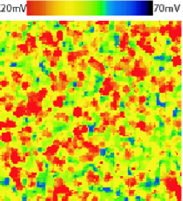
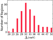
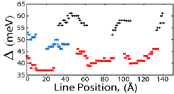
To understand how nanoscale variations of the superconducting energy gap can affect optical properties, we have applied an Effective Medium Approximation (EMA) to an inhomogenous system with a distribution of superconducting energy gaps. The merit of this approach is that we do not commit ourselves to any particular microscopic model of the inhomogeneity, but rather examine the macroscopic electrodynamics with a minimum of assumptions. In order to consider the case of the high superconductors, we include d-wave gap symmetry in our calculations and model the gap distribution based on BSCCO STM gap maps of Refs. Lang et al. (2002); McElroy et al. (2005a). As can be seen in these and other references, using STM to image a surface allows for mapping of high and low regions of superconducting gap magnitude, . The lattice structure of the BSCCO compounds is such that the surface can cleave smoothly between adjacent Bi-O planes, resulting in what should be a uniform surface structure. However, despite the supposed uniform lattice structure - that is to say there is no evidence of restructuring on the surface after cleaving - there is a spatially inhomogeneous energy gap structure at the surface. These inhomogeneous gap structures are commonly displayed in the form of a gap map, as seen in Fig. 1. In this figure, the blue patches are regions with a gap magnitude of about 50 meV and the red have gap values of about 20 meV. The largest number of regions occur with a gap of meV and the variation away from this value is about as indicated in Fig. 1. The diameters of these regions are typically of order 3 nm,McElroy et al. (2005b) but there is no particular pattern or underlying structure, rather the regions appear to be randomly distributed. It is also important to note the discontinuous nature of these gap maps, as can be seen in Fig. 2, where a scan along a line across the surface is shown. Here we see that the gap map contains distinct regions with nearly uniform gap values and consequently does not represent a smoothly varying single gap function , but rather suggests separate patches, each with its own gap value. In implementing the EMA as a phenomenological model, we are assuming that these STM images directly reflect the bulk gap distribution in an attempt to find signatures of this gap inhomogeneity. However, in the following, our results for far-infrared optical conductivity will show that no strong signatures were observed in mixtures of d-wave superconductors and indeed the results of the EMA can be very well approximated by a single spatially averaged gap value, which provides support for the past and continuing use of theories and data analyses which assume a spatially homogeneous energy gap in the bulk of high- superconductors. It would appear from our work that even if the inhomogeneities are present in the bulk, this assumption will be robust. On the other hand, we find that signatures in mixtures of s-wave superconductors present themselves in the form of a distribution of gap onsets over the range of gaps. This distribution results in an optical conductivity and optical self-energy which are distinct from a single gap system, and that are highly dependent upon the range of variation in the gap as well as the actual distribution present. In the following section, we begin by presenting the theory for the EMA and its use to obtain the optical conductivity. In section III, we will present our results for d-wave superconductivity based on the distribution of gaps seen in STM. Section IV will then present results for s-wave superconductivity and we summarize our conclusions in section V.
II Effective Medium Theory
It is of interest to us to understand in which systems and on what energy scales we might expect to see indications of inhomogeneities in bulk optical properties in order to make generalizations on, or identify, inhomogeneities in new materials. For this reason, we seek a purely phenomenological method of examining these effects, and here we will turn to Bruggeman’s EMA Bruggeman (1935); Carr et al. (1985). This EMA has been rigorously tested and previously applied to both microscopic metallic and microscopic superconducting-normal mixturesStroud (1975); Stroud and Pan (1978); Stroud (1979); Landauer (1952); Garner and Stroud (1983). It has also been used more recently to modelBarabash and Stroud (2003a, b) the very low frequency optical response in the cuprates and to discuss, in particular, the THz data on BSSCO from Corson et al.Corson et al. (1999, 2000) In certain circumstances, an alternative choice of EMA might be used, the Maxwell-Garnet EMA,Carr et al. (1985) however, that EMA applies when there are a dilute set of regions embedded in a large uniform background, which is not the case seen here in the STM of Fig. 1. In the following, we wish to make a semi-classical approximation, treating the system classically as having randomly distributed regions, each a uniform superconducting material, with properties defined by non-classical BCS results. The implicit assumption here is the randomness of the distribution of regions, since it has yet to be understood how and if these inhomogeneities are distributed throughout the bulk material.
For understanding the optical response of the entire system, we now summarize the idea of the EMA. An electromagnetic wave, of frequency , moving through a composite material will undergo multiple scattering and absorption events. In a bulk material these events are accounted for as an average by means of an effective complex dielectric function . If the bulk material is a composite, it is assumed to be composed of a number of regions of uniform dielectric functions . The scattering caused by these regions is dependent upon both the shape and size of the regions (grains). These scattering events can be taken into account by allowing each grain to become polarized, producing its own additional field. When we extend this to a macroscopic system, we add the constraint that the entire material should have a zero net polarization, i.e.Landauer (1952)
| (1) |
where is the relative fraction of the occurance of a certain type of grain indexed by and is that constituent’s polarization. Knowing this, we can solve for the real and imaginary parts of in the following equation:
| (2) |
where is the depolarization factor, determined by the shape of the constituent grain.Carr et al. (1985); Stroud (1975) The form of the polarization in Eq. (2) can be seen as the electric dipole contribution of a multipole expansion. Subsequent terms in the polarization (magnetic dipole, electric quadrupole, etc.) scale as functions of the grain size. In the spherical case these terms scale as where is the radius of the individual grains and is the wavelength of the field. For this case, the correction to Eq. (2) to next order would be:
| (3) |
We can see certain limits where the second term can be neglected.
In the small grain limit, we would expect the far-infrared (long wavelength
limit) response to be completely dominated by the first term. As this is
the region of interest for detecting signatures of the superconducting energy gap,
the EMA as in Eq. (2), with g set to a value of 1/3 (spherical grains), is appropriate for our purpose.
To implement the above EMA, we require the frequency dependent complex
conductivity as the
dielectric function can be written as , where
is the high frequency dielectric constant.
The constituent conductivities that we use for our purpose
here are calculated according to Zimmermann et al.,Zimmermann et al. (1991)
for the case of BCS s-wave superconductors with variable impurity scattering
and according to Schürrer et al.,Schürrer et al. (1998) for the BCS d-wave case.
In this paper,
we consider only an elastic scattering rate in the optical
conductivity and have not included inelastic scattering, as might
arise due to electron-boson interactions, such as phonons and spin fluctuations.
For a system of different types of superconducting grains,
the EMA of Eq. (2) can be expanded to the form of an
order complex polynomial in or by setting
( and ) as a
complex polynomial in . For example,
in we now have:
| (4) |
where the coefficients vary based on the choice of . For an system, one can solve directly for by substituting in its complex form, and solving for the real and imaginary parts separately. Analytically, this becomes largely unfeasible for . For this reason, considerations of composites, with a large number of constituents, , have not been thoroughly explored. Numerical solutions, however, are much more feasible. All that is required is solving for the set of ’s for each choice of N. This turns out to be a difficult task for and it is preferable to use a program to solve this algebraically. For example, for the N=2 case:
| (5) | |||||
| (6) |
where . We can see that these coefficients depend on the dielectric function (or conductivity) of each constituent, as well as their relative volume fractions and the depolarization factor, . These are the key pieces of information required to perform such an effective medium calculation, and as such, will be explained in detail for each case we wish to examine. Knowing the numerical coefficients, in Eq. 4, reduces the EMA calculation to the problem of numerically solving an Nth order complex polynomial. Such a polynomial has N solutions, of which only one is generally completely physical as must be strictly positive for each choice of .
III D-wave Energy Gap Inhomogeneities
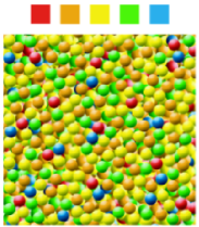
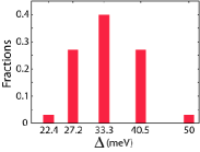
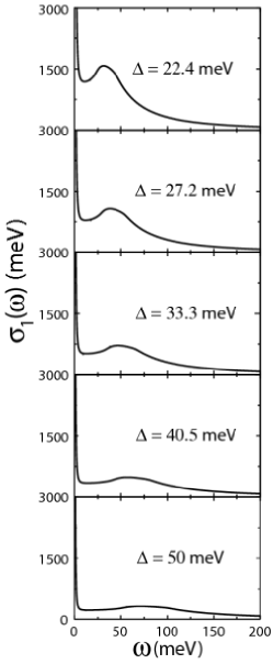
In order to determine possible signatures in the bulk due to the inhomogeneities seen by STM, we created a mixture of superconducting patches which is motivated by Fig. 1 and shown schematically in Fig. 1. We tried to maintain the same gap distribution seen in experiment and shown in the histogram of Fig. 1, but have re-binned the distribution so that it gives only five fractions in order to reduce the complexity of the numerical calcuation. This is shown in Fig. 1. Furthermore, we assumed that each constituent has d-wave gap symmetry similar to what one would expect in the bulk BSCCO conductivityHwang et al. (2007a) and have used the BCS d-wave conductivity program of Ref. Schürrer et al. (1998) to provide the input conductivities to the EMA. The BCS conductivity, while missing the inelastic component, does exhibit similar qualitative features as seen in experimental results, and can be applied with a minimal number of parameters: the energy gap, ; the plasma frequency, ; the temperature, ; and the scattering parameter , where is the elastic scattering rate. Since we are interested in the effects of varying only the gap parameter and we wish to limit the parameter space, we compute the EMA using constituents with similar plasma frequencies and scattering rates, but a range of values. The real part of the input conductivities of the constituent superconducting grains are shown in Fig. 3. These curves were calculated with realistic parameters, as given in Ref. Schürrer et al. (1998), i.e., eV , meV, at K.
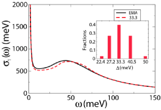
The overall characteristics of the resulting EMA in this case (shown in Fig. 4) remain what would be expected of a composite of a d-wave superconductor with scattering in the clean limit. Indeed, if we superimpose the conductivity curve for the average gap value, which dominates the gap distribution seen in STM, we find that there is not much difference between the two curves and therefore we conclude from these calculations that even if the inhomogeneity persists throughout the bulk, the size of variation in the gap, on scales seen in STM, cause very little variation in the overall conductivity of the sample from that of a single gap system, and therefore it is not possible to determine the presence of inhomogeneities from bulk far-infrared optical measurements. We note, as well, that variation in scattering rates of constituent grains (of up to a factor of 10) does not change the qualitative results of an EMA mixture with d-wave symmetry. We do not expect to have large values of the scattering rate, as this would quench the superconducting state, and there is no evidence from STM or otherwise for normal regions mixed in amongst the regions of inhomogeneous superconductivity at low temperatures. We conclude that the narrow range of gap values seen in STM coupled with the rather smooth nature of the conductivity for a BCS d-wave superconductor makes the observation of possible gap inhomogeneities uncertain through far-infrared optics. Adding in realistic inelastic scattering would not change this conclusion as this type of scattering will not introduce new sharp features in the conductivity. As a final point, most approaches to calculating optical properties of the cuprates assume a homogeneous model. Our results indicate that it is appropriate to compare results of such calculations for the average gap with experiment, and that ignoring inhomogeneities is a valid first approximation.
IV S-wave Energy Gap Inhomogeneities
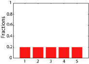
With the knowledge of the previous section, we are now motivated to find possible systems where gap inhomogeneities could have a clear signature in optics and indeed, it is clear that a system with a conductivity curve which contains sharp features would be an ideal candidate. Consequently, we now examine the effect of a distribution of gaps on a conventional s-wave BCS superconductor. We begin by calculating the zero temperature BCS s-wave conductivities for two simple distributions of gap values shown in Figs. 5 and 5. We have assumed a constant elastic scattering rate meV, and plasma frequency eV for all grains and this puts the system in the regime where , which is a mildly dirty limit. We calculate this EMA mixture under the assumption that each constituent maintains the same overall transition temperature, therefore, variations in value can be seen as analogous to changing the ratio from 3.53 7.53 in steps of 1. Curves for the real part of the conductivity, used for input to the EMA, are shown in Fig. 5.
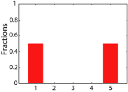
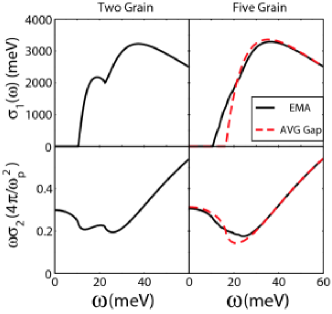
In the two grain composite, Fig. 6 (left column), we observe that the separation of gap onsets is sufficient to clearly display a two-gap result in the real part of the conductivity, (top frame). The real part of the conductivity rises sharply out of zero as it does in all of the curves in Fig. 5. This is followed by a first peak, after which a second rise begins at twice the value of the largest gap in our two gap distribution. A second peak follows at higher energy before the normal state Drude form is recovered. This is fundamentally different from, and should not be confused with, a two-band superconductor such as MgB2.Nicol and Carbotte (2005) It should be noted that the EMA is distinct in this two-gap system from a fractional average of its constituents since both and depend on both the real and imaginary parts of the constituents. In other words, for a two component mixture labeled and , where and , the EMA results in and . This additional dependence of the real part of the conductivity on the imaginary parts of its constituents in general leads to an increased low frequency contribution to from the imaginary conductivities (physically seen as scattering from constituents). The imaginary part multiplied by , namely , is shown in the lower left panel. As the frequency goes to zero, we find the inverse square of the London penetration depth for the composite system. At finite frequency, there are structures in corresponding to the frequencies of the onset of absorption of each of the two grains included in the model. These structures would be easily identifiable.
When we consider a less-separated five-grain distribution [seen in Fig. 5, with results in Fig. 6 (right column)], we immediately recognize the loss of clear onset points for each gap value and instead see a broadened rise in (Fig. 6, top right frame), which quickly rejoins an average gap fit at frequencies just above the highest point. Shown here is the EMA calculation as the solid black curve with the dashed red curve being the calculation for a single gap system using the average gap of the distribution as the input gap. It is clear that in this more realistic case the signature of inhomogeneities is not as readily identifiable as for the two gap case. This is also true for the imaginary part, , shown in the lower frame; now a single minimum is seen similar to the single gap case, but somewhat more broadened.
The real and imaginary parts of the conductivity are not the only optical quantities that enter a more modern discussion of the subject. In fact, it has been found to be very useful to introduce an optical self-energy defined in terms of the generalized Drude formula for the optical conductivity, , which is written as:Carbotte et al. (2005); Götze and Wölfle (1972); Mori et al. (2008)
| (7) |
Here is the plasma frequency and has both a real and imaginary part related, respectively, to a frequency dependent optical effective mass, , (where is the bare electron mass) and scattering rate, , given by:
| (8) |
and
| (9) |
An optical mass renormalization parameter, , is then defined by . These quantities are analogous, but different from, the quasiparticle mass renormalization and scattering rate which follow from the quasiparticle self-energy . Instead, is a two-particle quantity Hwang et al. (2007b). It is related to the Kubo formula for the current-current correlation function which determines . In general, as stated, the optical and quasiparticle mass renormalization and scattering rate are not the same, although in some limits they can be. As an example, the zero frequency mass renormalization and are equal. In the end, of course, contains exactly the same information as does . In fact, one can solve for and in terms of and to find:Carbotte et al. (2005); Götze and Wölfle (1972)
| (10) |
and
| (11) |
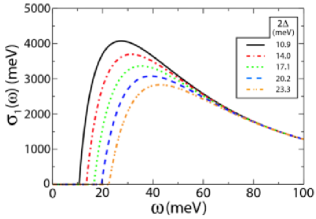
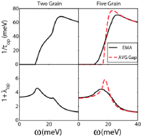
This does not mean, however, that these quantities have no particular value of their own. It is well documented that they can speak more directly to certain questions than can itself. For example, provides information on absorption and, in an s-wave superconductor, at zero temperature it is zero for photon energies, , less than twice the gap. A coherence peak is seen above this energy and at high we recover a measure of the normal state elastic scattering. Further, it has recently been found that in the underdoped cuprates, the real part of possesses a “hat like” structure which extends in energy over a range of about twice the pseudogap energy. This characteristic structure, which is superimposed on a large smooth incoherent background is nevertheless unmistakable and provides a direct image of pseuodogap formation Hwang et al. (2008) as it enters the in-plane optical data. By contrast, the effect of the opening of a pseudogap in the real and imaginary part of the conductivity is much more subtle and is spread over a much larger energy range. Thus, the optical quantities defined in Eq. (10) and (11) have proved useful and here we will consider how they are changed in the case of a distribution of regions of distinct gap values. In the top row of Fig. 7 we show results for (solid black curve) in meV as a function of (also in meV), for the two- and five-gap distributions of Figs. 5 and 5. The onset of scattering starts at the lowest value of twice the gap which is roughly 11 meV in our model. Also shown for comparison (dashed red curve) are results for the case of a homogeneous superconductor with the same average gap value. We see that, by comparison, the rise in in the inhomogeneous case, is much less steep and proceeds more gradually, being spread out over an energy scale which corresponds to the spread in gap values in our model distribution. The peak in the red dashed curve has its origin in the well known coherence peak of the BCS s-wave electronic density of states. In the normal state, would be independent of and equal to the input constant impurity scattering rate of 50 meV in this example. This is the value to which (superconducting) tends towards for greater than a few times the gap. In the superconducting state, however, no scattering is possible below twice the gap, at which energy it rises sharply and overshoots its normal state value, not because the intrinsic scattering potential has increased but rather because there are more final states available for scattering. For the inhomogeneous case this feature is simply smeared out somewhat because of the distribution of different superconducting regions which are sampled.
In the lower row of Fig. 7 we show our results for the optical mass enhancement parameter in the two- and five-gap cases. The solid black curve is for the inhomogeneous case and the red dashed curve is the homogeneous case with an averaged gap value for comparison. We note the inhomogeneities smear out the peak in around . However, in all other aspects the curves are similar. We emphasize two points. First, for large compared with the gap, the mass renormalization factor tends towards zero, which agrees with its normal state value. At however, is seen to be quite large (2.5) in both the homogeneous and inhomogeneous cases. In this limit, the optical effective mass has a very definite meaning. It is the value of the electron mass that one is to give the electrons if one wishes to use the classical London formula for the penetration depth at T=0, namely where n is the free electron density, e the electron charge and c the velocity of light. In the clean limit, i.e., no elastic scattering, would be the bare electron mass. Including impurities in BCS theory reduces the London penetration depth and this can be expressed by changing to in the conventional expression. Our results show that this result is only slightly changed in the inhomogeneous case, i.e. is only very slightly larger. The main effect of inhomogeneities manifests itself at finite frequency in the region of twice the gap. We see that, as compared with the dashed red curve, the solid black curve shows a much broader peak which is a direct consequence of spatial gap variations. The peak in around twice the gap is directly tied to the rapid rise in at this same frequency, as these are Kramers-Kronig (KK) related, i.e., a step in the scattering rate at translates into a logarithmic singularity at in its KK transform. We note in passing that a recent optical study of MoGe (Ref. Tashiro et al. (2008)) has revealed such a smearing of coherence peaks in the thinnest films studied, which could be attributed to inhomogeneities, however, other evidence suggests otherwise.
V Summary and Conclusions
Optical absorption is a probe of bulk properties. Using effective medium theory, we have calculated the optical conductivity of a superconductor consisting of a random array of nanoscale regions having different magnitudes of superconducting gap. The superconductivity in each grain is described within a BCS model, and both s- and d-wave symmetry is considered. For simplicity, models consisting of two and five distinct gap values are examined in detail. For an s-wave superconductor, the real part of the optical conductivity is zero for frequencies below twice the gap, with the missing optical spectral weight transferred to the condensate. For d-wave, the region below is also depleted, although some absorption remains at all frequencies and there is no sharp threshold in vs . In this latter circumstance the conductivity of the composite system does not exhibit qualitatively different behaviour as compared with the single grain which would represent a clear signature of the bulk inhomogeneities. In fact, there is no quantitative differences between of the composite and the individual grains, and the electromagnetic response appears close to that for the average gap. By contrast, for an s-wave gap, the sharp absorption edge in at twice the gap which is characteristic of a uniform BCS superconductor becomes less steep reflecting the onset of a distribution of gaps rather than of a single one. For a distribution involving only two well separated gap values, each is seen distinctly in both the real and imaginary parts of the conductivity as well as in the real and imaginary parts of the corresponding optical self energy. This latter property follows directly from a knowledge of the conductivity and has been found useful in past discussions of, for example, boson structures in optical properties. For the case of a distribution of many gap values, the presence of each individual gap is less evident with showing rather gradual onset over a frequency range representative of the variation in gap values. In conclusion, signatures of nanoscale spatial inhomogeneities in the far-infrared optical conductivity are much more readily recognized for composites consisting of s-wave gap symmetry components than they are for those with d-wave gap symmetry. Indeed, the fact that the d-wave case appears to be unaffected by the existence of inhomogeneities in spite of their apparent presence in STM, gives support for the continued use of single gap models for calculation and analysis of optical conductivity in the high- cuprates.
Acknowledgements.
We thank Ewald Schachinger and Ricardo Lobo for providing some of the computer programs used in this work. We also thank Kyle McElroy for providing us with the gap map of Fig.1 and Clare Armstrong for assistance with the schematic diagram of Fig. 1. This work has been supported by the Natural Sciences and Engineering Council of Canada (NSERC) and the Canadian Institute for Advanced Research (CIFAR).References
- Pan et al. (2001) S. Pan, J. P. O’Neal, R. L. Badzey, C. Chamon, H. Ding, J. R. Engelbrecht, Z. Wang, H. Eisaki, S. Uchida, A. K. Gupta, et al., Nature (London) 413, 282 (2001).
- Lang et al. (2002) K. M. Lang, V. Madhavan, J. E. Hoffman, E. W. Hudson, H. Eisaki, S. Uchida, and J. C. Davis, Nature (London) 415, 412 (2002).
- Howald et al. (2003) C. Howald, H. Eisaki, N. Kaneko, M. Greven, and A. Kapitulnik, Phys. Rev. B 67, 014533 (2003).
- Fang et al. (2006) A. C. Fang, L. Capriotti, D. J. Scalapino, S. A. Kivelson, N. Kaneko, M. Greven, and A. Kapitulnik, Phys. Rev. Lett. 96, 017007 (2006).
- Gomes et al. (2007) K. K. Gomes, A. N. Pasupathy, A. Pushp, S. Ono, Y. Ando, and A. Yazdani, Nature (London) 447, 569 (2007).
- McElroy et al. (2005a) K. McElroy, D. H. Lee, J. E. Hoffman, K. M. Lang, J. Lee, E. W. Hudson, H. Eisaki, S. Uchida, and J. C. Davis, Phys. Rev. Lett. 94, 197005 (2005a).
- McElroy et al. (2005b) K. McElroy, J. Lee, J. A. Slezak, D.-H. Lee, H. Eisaki, S. Uchida, and J. C. Davis, Science 309, 1048 (2005b).
- Pasupathy et al. (2008) A. N. Pasupathy, A. Pushp, K. K. Gomes, C. V. Parker, J. Wen, Z. Xu, G. Gu, S. Ono, Y. Ando, and A. Yazdani, Science 320, 196 (2008).
- Kato et al. (2005) T. Kato, S. Okitsu, and H. Sakata, Phys. Rev. B 72, 144518 (2005).
- Niestemski et al. (2007) F. C. Niestemski, S. Kunwar, S. Zhou, S. Li, H. Ding, Z. Wang, P. Dai, and V. Madhavan, Nature (London) 450, 1058 (2007).
- Hoogenboom et al. (2003) B. W. Hoogenboom, K. Kadowski, B. Revaz, and O. Fischer, Physica C 391, 376 (2003).
- Bobroff et al. (2002) J. Bobroff, H. Alloul, S. Ouazi, P. Mendels, A. Mahajan, N. Blanchard, G. Collin, V. Guillen, and J.-F. Marucco, Phys. Rev. Lett. 89, 157002 (2002).
- Loram et al. (2004) J. W. Loram, J. L. Tallon, and W. Y. Liang, Phys. Rev. B 69, 060502(R) (2004).
- Andersen et al. (2006) B. M. Andersen, A. Melikyan, T. S. Nunner, and P. J. Hirschfeld, Phys. Rev. B 74, 060501(R) (2006).
- Bruggeman (1935) D. Bruggeman, Ann. Phys. (Leipz.) 24, 636 (1935).
- Carr et al. (1985) G. Carr, S. Perkowitz, and D. Tanner, in Infrared and Millimeter Waves, edited by K. J. Button (Academic Press, 1985), vol. 13, pp. 171–263.
- Stroud (1975) D. Stroud, Phys. Rev. B 12, 3368 (1975).
- Stroud and Pan (1978) D. Stroud and F. P. Pan, Phys. Rev. B 17, 1602 (1978).
- Stroud (1979) D. Stroud, Phys. Rev. B 19, 1783 (1979).
- Landauer (1952) R. Landauer, J. Appl. Phys. 23, 7 (1952).
- Garner and Stroud (1983) J. Garner and D. Stroud, Phys. Rev. B 28, 2447 (1983).
- Barabash and Stroud (2003a) S. V. Barabash and D. Stroud, Physica B 338, 224 (2003a).
- Barabash and Stroud (2003b) S. V. Barabash and D. Stroud, Phys. Rev. B 67, 144506 (2003b).
- Corson et al. (1999) J. Corson, R. Mallozzi, J. Orenstein, J. N. Eckstein, and I. Bozovic, Nature (London) 398, 221 (1999).
- Corson et al. (2000) J. Corson, J. Orenstein, S. Oh, J. O’Donnell, and J. N. Eckstein, Phys. Rev. Lett. 85, 2569 (2000).
- Zimmermann et al. (1991) W. Zimmermann, E. H. Brandt, M. Bauer, E. Seider, and L. Genzel, Physica C 183, 99 (1991).
- Schürrer et al. (1998) I. Schürrer, E. Schachinger, and J. P. Carbotte, Physica C 303, 287 (1998).
- Hwang et al. (2007a) J. Hwang, T. Timusk, and G. D. Gu, J. Phys. : Condens. Matter 19, 125208 (2007a).
- Nicol and Carbotte (2005) E. J. Nicol and J. P. Carbotte, Phys. Rev. B 71, 054501 (2005).
- Carbotte et al. (2005) J. P. Carbotte, E. Schachinger, and J. Hwang, Phys. Rev. B 71, 054506 (2005).
- Götze and Wölfle (1972) W. Götze and P. Wölfle, Phys. Rev. B 6, 1226 (1972).
- Mori et al. (2008) T. Mori, E. J. Nicol, S. Shiizuka, K. Kuniyasu, T. Nojima, N. Toyota, , and J. P. Carbotte, Phys. Rev. B 77, 174515 (2008).
- Hwang et al. (2007b) J. Hwang, E. J. Nicol, T. Timusk, A. Knigavko, and J. P. Carbotte, Phys. Rev. Lett. 98, 207002 (2007b).
- Hwang et al. (2008) J. Hwang, J. P. Carbotte, and T. Timusk, Phys. Rev. Lett. 100, 177005 (2008).
- Tashiro et al. (2008) H. Tashiro, J. M. Graybeal, D. B. Tanner, E. J. Nicol, J. P. Carbotte, and G. L. Carr, arXiv:0803.1185 (2008).