Tunable Graphene Single Electron Transistor
Abstract
We report electronic transport experiments on a graphene single electron transistor. The device consists of a graphene island connected to source and drain electrodes via two narrow graphene constrictions. It is electrostatically tunable by three lateral graphene gates and an additional back gate. The tunneling coupling is a strongly nonmonotonic function of gate voltage indicating the presence of localized states in the barriers. We investigate energy scales for the tunneling gap, the resonances in the constrictions and for the Coulomb blockade resonances. From Coulomb diamond measurements in different device configurations (i.e. barrier configurations) we extract a charging energy of 3.4 meV and estimate a characteristic energy scale for the constriction resonances of 10 meV.
pacs:
71.10.Pm, 73.21.-b, 81.05.Uw, 81.07.TaThe recent discovery of graphene nov04 ; gei07 , filling the gap between quasi 1-dimensional (1-D)
nanotubes
and 3-D graphite
makes truly 2-D crystals accessible and links solid state devices to molecular electronics joa00 .
Graphene, which exhibits unique electronic properties including massless carriers near the Fermi level and potentially weak spin orbit and hyperfine couplings min06 ; tom07 has been
proposed to be a promising material for spin qubits tra07 , high mobility electronics che07 ; han07 and it may have the potential to contribute to the downscaling of state-of-the-art silicon technology ieo04 .
The absence of an energy gap in 2-D graphene and phenomena related to Klein tunneling dom99 ; kat06 make it hard to confine carriers electrostatically and to
control transport on the level of single particles.
However, by
focusing on graphene nanoribbons, which are known to exhibit an effective transport gap che07 ; han07 ; sol07 ; dai08 this limitation can be overcome. It has been shown recently that such a transport gap allows
to fabricate well tunable graphene nanodevices sta08 ; pon08 ; mia07 . Here we investigate a fully tunable single electron transistor (SET) that consists of a width modulated graphene structure exhibiting spatially separated transport gaps. SETs consist of a conducting island connected by tunneling barriers to two conducting leads. Electronic transport through the device can be blocked by Coulomb interaction for temperatures and bias voltages lower than the characteristic energy required to add an electron to the island kou97 .
The sample is fabricated based on single-layer graphene flakes obtained from mechanical exfoliation of bulk graphite. These flakes are deposited on a highly doped silicon substrate with a 295 nm silicon oxide layer nov04 .
Electron beam (e-beam) lithography is used for patterning the isolated graphene flake by subsequent Ar/O2 reactive ion etching.
Finally, an additional e-beam and lift-off step is performed to pattern Ti/Au (2 nm/50 nm) electrodes.
For the detailed fabrication process and the single-layer graphene verification we refer to Refs. sta08 ; fer06 ; dav07a .
Fig. 1a shows a scanning force micrograph of the investigated device. Both the metal electrodes and the graphene structure are highlighted.
In Fig. 1b, a schematic illustration of the fabricated graphene SET device is shown. Source (S) and drain (D) contacts connect via 50 nm wide constrictions to the graphene island. The two constrictions are separated
by 750 nm and the island has an area m2 (see Figs. 1a,b).
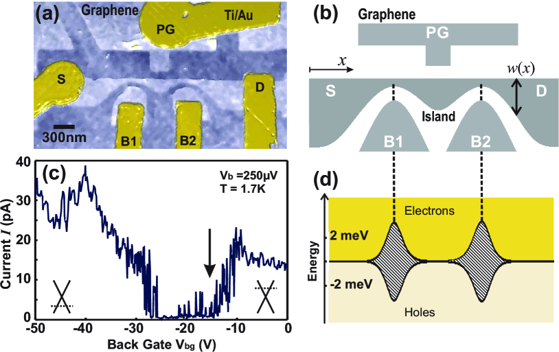
In order to tune the two tunneling barriers and the island electrostatically and independently, three lateral graphene gates mol07 have been fabricated closer than 100 nm to the active graphene structure (see Fig. 1a). These are the two barrier gates B1 and B2, and the plunger gate PG (Fig. 1b). The additional highly doped silicon substrate is used as a back gate (BG) to adjust the overall Fermi level ().
All measurements have been performed in a variable temperature 4He cryostat at a base temperature of T 1.7 K and the sample was heated to 135∘C in vacuum for 12 h before cooling down. We have measured the two-terminal conductance through the graphene SET device by applying a symmetric DC bias voltage while measuring the current through the SET device with a resolution better than 10 fA. For differential conductance measurements a small AC bias, V has been superimposed on and the differential conductance has been measured with lock-in techniques.
At small bias (V) strong current suppression is observed at V V, as shown in Fig. 1c. This suppression is in agreement with earlier studies of graphene nanoconstrictions che07 ; han07 . It can be interpreted as a transport gap forming around the back gate voltage where the system is charge neutral. Hole transport occurs at V, electron transport at V.
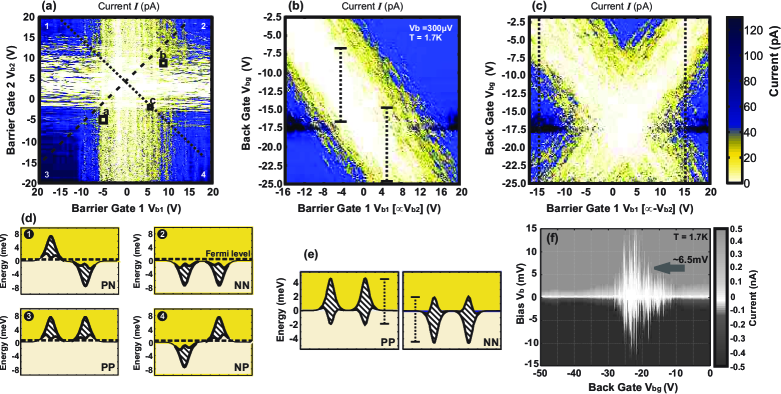
Measurements for varying back gate voltage (Fermi level) and bias voltage allow to estimate the size of the transport gap as shown in Fig. 2f. A value of the order of meV is found. However, the strong modulation of the current shows, that localized states lead to strong transmission resonances. Therefore we refer in the following to an ”effective” energy gap or a transport gap.
The geometric design of our structure (see Fig. 1a) gives local electrostatic access to the constriction regions. Fig. 2a shows a measurement of the current where the voltages and on the two barrier gates B1 and B2 have been independently tuned while the back gate voltage was kept fixed at V. A vertical and a horizontal stripe of suppressed current is observed. This observation indicates that transport through each of the two constrictions is characterized by a transport gap which can be individually tuned with the respective barrier gate. For example, keeping V constant and sweeping from -20 V to + 5 V keeps constriction 1 conducting well while constriction 2 is tuned from large conductance to very low conductance (into the transport gap). The capacitive cross talk from B1 to constriction 2, and from B2 to constriction 1 is found to be smaller than 2.
These measurements suggest that the energy diagram shown in Fig. 1d is a useful description of the data. In this figure, high (electron) and low (hole) energy states are separated by two solid lines. Outside the constriction regions these lines are degenerate and represent the energy of the charge neutrality point in graphene. In the constriction regions the two lines are energetically separated indicating the observed effective energy (transport) gap by hatched areas. As a result of the lack of an energy gap of the two-dimensional graphene material, the exact shape of the effective ( is the transport direction) is given only by lateral confinement, i.e., by the variation of the width along the device. We assume that electron-hole symmetry holds in the confined geometry and therefore plot an effective conduction band edge at , and an effective valence band edge at .
It is known from earlier experiments che07 ; han07 that graphene nanoribbons (or constrictions) exhibit an effective energy gap. For ribbons of width nm the size of this gap scales according to , where m/s is the Fermi velocity. The energy gap for nanoribbons wider than 20 nm can be reasonably well described by sol07 , where eVnm and nm-1 are constants extracted from fits of the experimental data in Ref. han07 . Within this model the width of our graphene structure translates to an effective transport band structure exhibiting two tunnel junctions with barrier height meV and an almost gap free island (eV) as shown in Fig. 1d. According to the model the SET is expected to be operational in the regime of . The measured transport gap agrees reasonably well with the modeled barrier height, as indicated by the arrow in Fig. 2f.
The local electrostatic influence of the gate electrodes can be incorporated into this heuristic description as a local shift of the energy of the charge neutrality point described by smooth characteristic potentials () which may be derived from purely electrostatic considerations. While is independent of , and are peaked at the respective constrictions, and is peaked within the island. For creating the schematic figures in this paper [Figs. 1(d), 2(d), (e)] we have used a convenient peaked function (the shape of which is irrelevant for this simple discussion) with peak heights compatible with lever arms extracted from the experiment (see below).
Having established a heuristic energy diagram describing our sample we now return to the discussion of the measurement in Fig. 2a which is facilitated by the diagrams in Fig. 2d. In this measurement V. From Fig. 1c we deduce that the Fermi energy in the contacts of the structure lies within the conduction band, as indicated by the horizontal dashed lines in the four drawings in Fig. 2d. The four drawings represent energy diagrams corresponding to the four corners of Fig. 2a as indicated by the white numbers. In corner 2 transport takes place in the conduction band throughout the whole structure. In corner 1 (4) transport occurs in the conduction band in the right (left) part of the structure. The left (right) constriction is traversed via states in the valence band. The situation is even more complex in corner 3, where the Fermi energy cuts both barrier regions in the valence band. Although these situations imply two or even four p-n-like transitions along the structure, no distinctive features are observed in our measurements. This may be a manifestation of the suppression of backscattering due to Klein tunneling.
Figs. 2b and 2c demonstrate the consistency of our heuristic model with the experimental observations. Fig. 2b shows the current measured as a function of and , with being simultaneously swept such that V (see dashed line in Fig. 2a). In this way the barrier regions are simultaneously shifted up or down (see Fig. 2e). Fig. 2b shows that the transport gap measured as a function of the back gate is shifted correspondingly, with .
Fig. 2c shows the current measured as a function of and , with being simultaneously swept such that V (see dotted line in Fig. 2a). For V (vertical dashed lines in Fig. 2c) the position of the gaps in energy correspond to diagrams 1 and 4 in Fig. 2d. In these two cases, sweeping the back gate allows to probe the two spatially separated transport gaps individually.
If we focus on a smaller voltage scale much more finestructure in the parameter plane appears, as shown in Fig. 3. Subplots 3a-c are different close ups of Fig. 2a (see black labeled boxes therein).
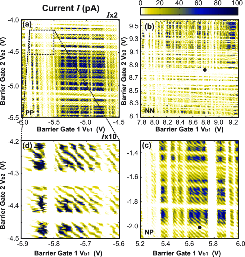
Although Figs. 3a-c show the current in three different regimes the transport characteristics do not differ significantly. Here, we distinguish between the PP (Fig. 3a), NN (Fig. 3b) and the NP (Fig. 3c) regime, depending on either having the tunnel barriers (according to B1 and B2) shifted down (N) or up (P). We observe in all regimes (Fig. 3) sequences of horizontal and vertical stripes of suppressed current and current resonances. Their direction in the - plane indicates that their physical origin has to be found within constriction 1 (vertical stripes) or constriction 2 (horizontal stripes). A blow-up of a small region in Fig. 3a is shown in Fig. 3d. The current exhibits even finer resonances which are almost equally well tuned by both constriction gates. We therefore attribute these resonances to states localized on the island between the barriers. It will be shown below that these resonances occur in the Coulomb blockade regime of the island. We attribute the deviations from perfectly straight diagonal lines to the presence of rough edges and inhomogeneities within the graphene island which has dimensions (slightly) larger than the elastic mean free path.
This characteristic pattern (Fig. 3d) can be found within a large - parameter range within the regime where the two barrier gaps cross each other (i.e. the inner bright part of Fig. 2a).
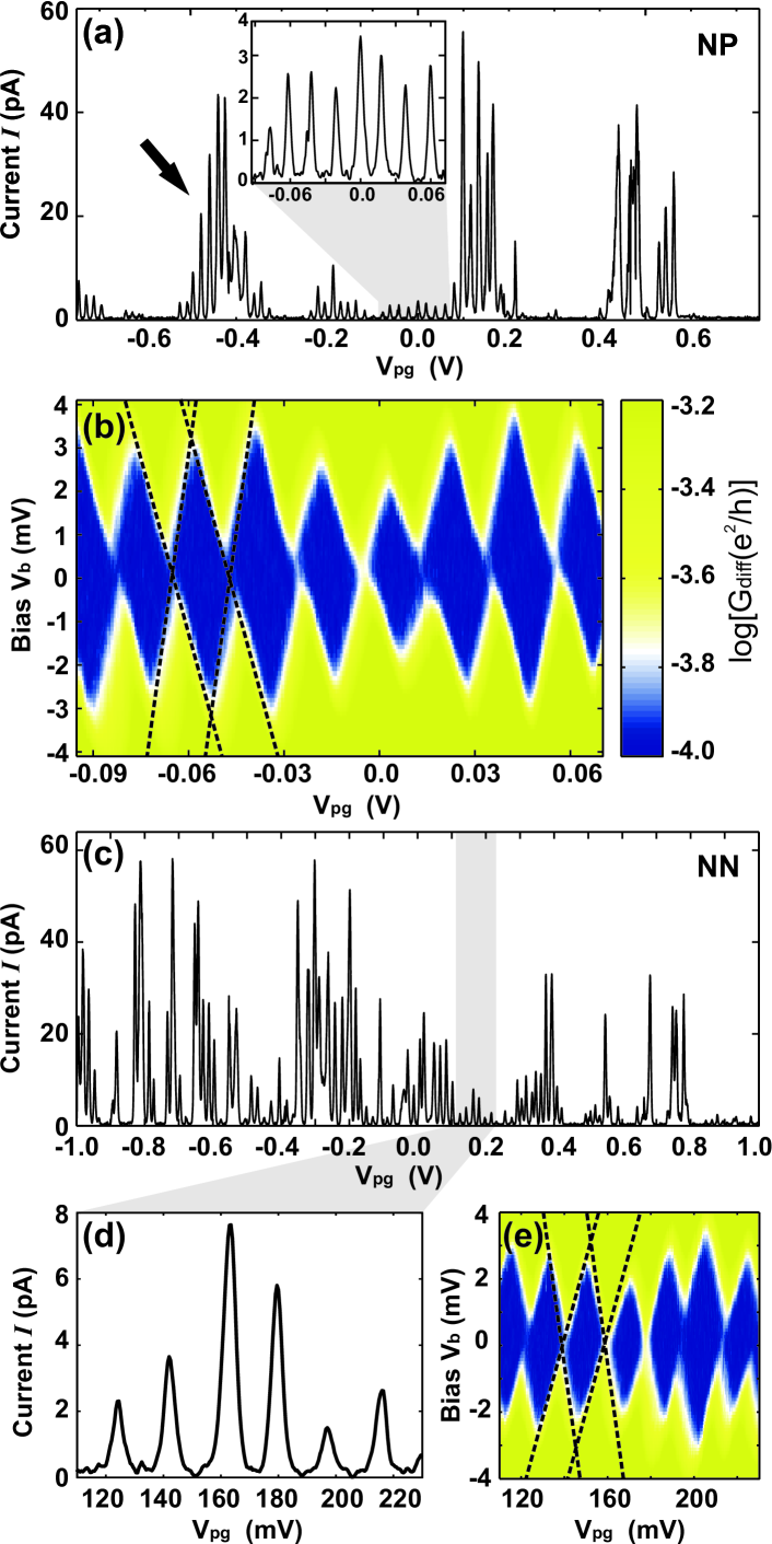
So far we mainly focused on the barriers and in the following we concentrate on the charging of the island itself. We fix the barrier gate potentials ( and ) either in the NN regime or in the NP regime in order to study Coulomb blockade. Fig. 4a shows sharp conductance resonances with a characteristic period of about 20 mV (=5.570 V, and =-2.033 V are fixed). Their amplitude is modulated on a much larger voltage scale of about 200 mV by the transparency modulations of the constrictions (cf. Fig. 3d). These resonances in the narrow graphene constrictions can significantly elevate the background of the Coulomb peaks (see e.g. black arrow). The inset of Fig. 4a confirms that transport can also be completely pinched off between Coulomb blockade peaks. Corresponding Coulomb diamond measurements kou97 , i.e., measurements of the differential conductance () as function of bias voltage and plunger gate voltage are shown in Fig. 4b. Within the swept plunger gate voltage range no charge rearrangements have been observed and the peak positions were stable over more than 10 consecutive plunger gate sweeps.
In Fig. 4c we show conductance resonances, which have been measured within the NN regime (for fixed V and V, see Fig. 3b). The range shown here is wider than in Fig. 4a. Again we observe (i) strong transport modulations on a scale of about 100 mV, which originate from resonances within the barriers and (ii) Coulomb peaks on a scale of about 20 mV which are blown up in Fig. 4d. The corresponding Coulomb diamond measurements (Fig. 4e) are similar to those measured in the NP regime (Fig. 4a). The Coulomb peaks (Fig. 4d and inset in Fig. 4a) and the Coulomb diamonds are not very sensitive to the tunnel barrier regime, although in one case a p-n-like junction should be present, whereas in the other case a more uniform island is expected.
From the extent of all the diamonds in bias direction we estimate the average charging energy of the graphene single electron transistor operated in both regimes to be meV. This charging energy corresponds to a sum-capacitance of the graphene island aF, whereas the extracted back gate capacitance aF is higher than the purely geometrical parallel plate capacitance of the graphene island aF. This is related to the fact that the diameter of the graphene island () is approximately the same as the gate oxide thickness sta08 ; ihn04 .
| BG | PG | B1 | B2 | Source (S) | Drain (D) | |
|---|---|---|---|---|---|---|
| Capacitance (aF) | 18.0 | 6.9 | 6.0 (5.5) | 5.0 | 1.8 (10.1) | 9.6 (1.8) |
| Lever arm | 0.38 | 0.15 | 0.13 (0.12) | 0.1 | 0.04 (0.21) | 0.20 (0.04) |
The lever arms, and the electrostatic couplings of the electrodes to the graphene island do not change significantly between the NN, PP (not shown) and the NP regime. Thus, the lever arm of the plunger gate is ( aF), whereas the electrostatic coupling to the other gates were determined to be aF and aF.
All lever arms and capacitances are summarized in Tab. 1. It shows that the island geometry and dot location with respect to the lateral gates stays almost constant. However, the capacitive coupling to the source and drain contacts (i.e. and ) changes significantly as function of the tunnel barrier configuration. This can be nicely seen when comparing the symmetry of the diamonds in the NN and NP regime as shown in Figs. 4e and 4b. While the size and fluctuations of the diamonds remain (almost) constant the lever arms of the source and drain contacts change strength. In one case (NP regime) we extract aF and aF, whereas in the other (NN regime) aF and aF, which can be seen from the different slopes of the diamond edges. However, the individual tunnel barriers strongly depend on the local barrier configuration and change also within the NN or the NP region.
We now estimate the energy scale of the resonances in the constrictions. The spacing of the constriction resonances in plunger gate is about 200 mV, whereas the spacing of Coulomb peaks is 20 mV. By assuming that the capacitance between the plunger gate and the localized states in the constrictions leading to the resonances is about three times smaller than (estimated from the geometry of the device) the energy scale of the resonances in the constriction is about 10 mV, in agreement with the measured gap in Fig. 2f.
Alternatively, this characteristic energy scale can also be estimated by considering that the back gate voltage sweep from -25 V to -15 V (around the charge neutrality point at -20 V, Fig. 1c) translates to a Fermi energy sweep over an energy interval of approx. 120 meV. Near the Dirac point the spacing of the constriction resonances in back gate voltage is found to be of the order of 200 mV leading again to a characteristic energy scale of 10 meV.
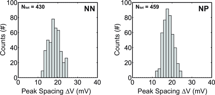
Finally, we also performed Coulomb peak spacing () statistics in both, the NN and NP regime with in total more than 900 Coulomb peaks, as shown in Fig. 5. The mean nearest neighbor spacing of the Coulomb peaks in both the NN and NP regime do not differ significantly (=17.4 mV and =17.9 mV). The broadening of the peak spacing distribution is in both cases significant ranging from 3.3mV (0.6 meV) to 2.5mV (0.5 meV), which is in agreement with Ref. pon08 . The broadening of the observed unimodal peak spacing distribution is significantly larger than the difference between the average spacings in the NN and NP regimes (0.075 meV). The inhomogeneity of the island, as indicated by the different slopes in Fig. 3d may significantly contribute to the observed broadening, which might be also partly influenced by the underlying modulation of the transmission through the narrow graphene constrictions. The broadening of the distributions is significantly larger than expected for a purely metallic SET for00 . On the other hand the width of the distribution is of the order of the estimated single-particle level spacing com03 , similar to previous observations in high-quality GaAs quantum dots Patel98 ; Luscher01 . This may indicate the importance of quantization effects.
In conclusion, we have fabricated and characterized a fully tunable graphene single electron transistor based on an etched width-modulated graphene nanostructure with lateral graphene gates. Its functionality was demonstrated by observing electrostatic control over the tunneling barriers. From Coulomb diamond measurements it was estimated that the charging energy of the graphene island is 3.4 meV, compatible with its lithographic dimensions. These results give detailed insights into tunable graphene quantum dot devices and open the way to study graphene quantum dots with smaller dimensions and at lower temperatures.
Acknowledgment — The authors wish to thank R. Leturcq, P. Studerus, C. Barengo, P. Strasser, A. Castro-Neto and K. S. Novoselov for helpful discussions. Support by the ETH FIRST Lab and financial support by the Swiss National Science Foundation and NCCR nanoscience are gratefully acknowledged.
References
- (1) K. S. Novoselov, A. K. Geim, S. V. Morozov, D. Jiang, M. I. Katsnelson, S. V. Dubonos, I. V. Grigorieva, A. A. Firsov, Science, 306, 666, (2004).
- (2) For review see: A. K. Geim and K. S. Novoselov, Nat. Mater. 6, 183 (2007), A. H. Castro Neto, F. Guinea, N. M. Peres, A. K. Geim, cond-mat 0709.1163v1 (2007).
- (3) C. Joachim, J. K. Gimzewski and A. Aviram, Nature, 408, 541, (2000).
- (4) H. Min, J. E. Hill, N. A. Sinitsyn, B. R. Sahu, L. Kleinman, and A. H. MacDonald, Phys. Rev. B, 74, 165310, (2006).
- (5) N. Tombros, C. Jozsa, M. Popinciuc, H. T. Jonkman and B. J. van Wees, Nature, 448, 571-574, (2007).
- (6) B. Trauzettel, D.V. Bulaev, D. Loss, and G. Burkard, Nature Physics, 3, 192, (2007).
- (7) Z. Chen, Y. Lin, M. Rooks and P. Avouris, Physica E, 40, 228, (2007).
- (8) M. Y. Han, B. Özyilmaz, Y. Zhang, and P. Kim, Phys. Rev. Lett., 98, 206805 (2007).
- (9) M. Ieong, B. Doris, K. Kedzierski, K. Rim and M. Yang, Science, 306, 2057 (2004).
- (10) N. Dombay, and A. Calogeracos, Phys. Rep., 315, 41 58 (1999).
- (11) M. I. Katsnelson, K. S. Novoselov, amd A. K. Geim, Nature Phys. 2, 620 625 (2006).
- (12) F. Sols, F. Guinea and A. H. Castro Neto, Phys. Rev. Lett., 99, 166803 (2007).
- (13) X. Li, X. Wang, L. Zhang, S. Lee, H. Dai, Science, 319, 1229 (2008).
- (14) C. Stampfer, J. Güttinger, F. Molitor, D. Graf, T. Ihn, and K. Ensslin, Appl. Phys. Lett., 92, 012102 (2008).
- (15) L. A. Ponomarenko, F. Schedin, M. I. Katsnelson, R. Yang, E. H. Hill, K. S. Novoselov, A. K. Geim, Science, 320, 356 (2008).
- (16) F. Miao, S. Wijeratne, Y. Zhang, U. C. Coskun, W. Bao, C. N. Lau, Science, 317, 1530 (2007).
- (17) L. P. Kouwenhoven et al. 1997, ”Electron transport in quantum dots”, Mesoscopic Electron Transport (ed) L. L. Sohn, L. P. Kouwenhoven and G. Schön (NATO Series, Kluwer, Dordrecht).
- (18) A. C. Ferrari, J. C. Meyer, V. Scardaci, C. Casiraghi, M. Lazzeri, F. Mauri, S. Piscanec, D. Jiang, K. S. Novoselov, S. Roth, and A. K. Geim, Phys. Rev. Lett. 97, 187401 (2006).
- (19) D. Graf, F. Molitor, K. Ensslin, C. Stampfer, A. Jungen, C. Hierold, and L. Wirtz, Nano Lett., 7, 238 (2007).
- (20) F. Molitor, J. Güttinger, C. Stampfer, D. Graf, T. Ihn, and K. Ensslin, Phys. Rev. B 76, 245426 (2007).
- (21) Here an offset of 5 V has been used in order to compensate the slightly different doping of the two narrow graphene constrictions. This offset can also be nicely seen at in Fig. 2c.
- (22) See Fig. 12.11 in T. Ihn, Springer Tracts in Modern Physics 192, Springer 2004, p. 102.
- (23) M. Furlan, T. Heinzel, B. Jeanneret, S. V. Lotkhov and K. Ensslin, Europhys. Lett., 49, 369 (2000).
- (24) The single level spacing is estimated by , where is the area of the graphene island and is the number of carriers on the island. For =10 to 100 electrons on the island we estimate a characteristic energy spacing of 0.75 meV to 0.24 meV.
- (25) S. R. Patel, S. M. Cronenwett, D. R. Stewart, A. G. Huibers, C. M. Marcus, C. I. Duruöz and J. S. Harris, Jr., K. Campman and A. C. Gossard, Phys. Rev. Lett. 80, 4522 - 4525 (1998)
- (26) S. Lüscher, T. Heinzel, K. Ensslin, W. Wegscheider, and M. Bichler, Phys. Rev. Lett. 86, 2118 (2001)