Ballistic Hot Electron Transport in Graphene
Abstract
We theoretically study the inelastic scattering rate and the carrier mean free path for energetic hot electrons in graphene, including both electron-electron and electron-phonon interactions. Taking account of optical phonon emission and electron-electron scattering, we find that the inelastic scattering time and the mean free path for electron densities . In particular, we find that the mean free path exhibits a finite jump at the phonon energy due to electron-phonon interaction. Our results are directly applicable to device structures where ballistic transport is relevant with inelastic scattering dominating over elastic scattering.
The existence SSC of gated two-dimensional (2D) graphene layers, where carrier transport controlled by an external gate has become possible N1 , provides the exciting possibility of novel high-speed electronic device structures app utilizing the high graphene carrier mobility N1 ; N2 . Such fast graphene devices would work in the ballistic transport regime, where carrier mobility limited by elastic scattering, is essentially irrelevant (i.e. , with , being respectively the elastic and the inelastic carrier mean free path), and what matters is the inelastic scattering due to electron-electron and electron-phonon interactions. Such ballistic devices for ultrafast applications can only work if the relevant device dimensions are smaller than the inelastic mean free path , and the speed of this device is limited by the inelastic scattering time (, where is the elastic relaxation time). In currently available high-mobility () graphene samples, , and therefore, inelastic scattering will dominate device operations for length (time) scales below .
In this Letter, we calculate the inelastic mean free path () and the corresponding inelastic scattering rate in graphene limited by electron-electron and electron-phonon interactions. Our study is motivated by electron transport in the hot electron transistor device structure which is so designed as to allow electrons to traverse the base region ballistically. In such a device scheme, highly energetic electrons are injected in the emitter region which then travel through the base region ballistically before reaching the collector region. The fraction of electrons that reach the collector goes as , where is the width of the base region. The mean free path is given by , where is the Fermi velocity of electron and is the inelastic scattering time, which, in general, is a strong function of the injected energy of electrons and the electron density in the base region.
We consider two principal mechanisms contributing to inelastic scattering arising from many-body interactions: (1) absorption or emission of optical phonons by electrons due to electron-phonon (e-ph) interaction; (2) exchange-correlation effects induced by electron-electron (e-e) interaction. For the e-ph interaction, we take into account the most dominant phonon mode in graphene – the LO phonons at the Brillouin zone center . This mode shows up as the ‘G peak’ resonance observed in Raman scattering experiments with a phonon energy Raman . Acoustic phonons couple very weakly to electrons in graphene, and the associated scattering rates are on the order of s-1 even at room temperature chen_phonon and can be ignored when compared to the scattering mecanism discussed above. We also neglect electron-impurity scattering in our calculation because the mean free paths of currently available high mobility graphene samples are much longer than the inelastic mean free paths to be calculated in this paper.
The inelastic scattering of electrons causes damping (i.e., decay) of the quasiparticle state, and the inelastic scattering lifetime is given by the imaginary part of the self-energy evaluated on the energy shell , where ( is the electron kinetic energy and is the Fermi velocity which is constant in graphene irrespective of electron density) is the single-particle energy rendered from the chemical potential . The inelastic scattering rate (or damping rate) consists of two contributions, given by , where the first term denotes the contribution to the self-energy due to electron-LO phonon interaction tsephonon ,
| (1) |
and the second term on the right denotes the contribution to the self-energy due to e-e Coulomb interaction dassarma_ee ,
| (2) | |||
Here, are the Bose and Fermi distribution functions, respectively. For the e-ph contribution Eq. (1), is the e-ph coupling constant Ando , where is a dimensionless constant characterizing the rate of change of the nearest-neighbor hopping energy with respect to bond length, is the equilibrium bond length, is the number of unit cells, is the mass of a carbon atom ( is the electron mass). For the Coulomb contribution Eq. (2), is the bare Coulomb interaction, is the dielectric function given, within the random phase approximation, by the electron polarizability Polar .


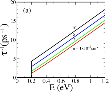
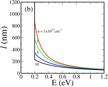
In the following, we calculate at zero temperature, which is a very good approximation for graphene since at the usual doping density , the corresponding Fermi temperature is much higher than room temperature. First we calculate the self-energy correction due to e-ph interaction, Eq. (1). Fig. 1(a) shows the scattering rate versus electron energy for different values of electron density. The gap from to (which is the LO phonon energy ) is a characteristic feature of the LO phonon absorption process; it results from the Pauli blocking by those electrons located within an amount of energy of the Fermi level, so that decay by electrons with energy is forbidden due to the restricted phase space. Beyond the gap, behaves linearly as due to the linear dependence on momentum of the graphene density of states, . As a result of the gap in , the calculated mean free path [Fig. 1(b)] is infinite within the range of the phonon energies, before falling off as with electron energy . Fig. 1 also shows that the scattering rate (mean free path) increases (decreases) with electron density, as scattering events become more frequent with increasing number of electrons.


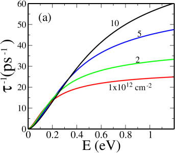
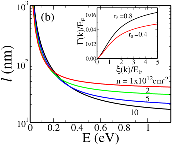
For e-e Coulomb interaction, we show the calculated inelastic scattering rate Eq. (2) and the corresponding inelastic mean free path, in Fig. 2. The strength of Coulomb interaction is characterized by the dimensionless coupling parameter , where is the effective background dielectric constant of the substrate Polar . In the inset of Fig. 2(b), the calculated damping rates are shown for different coupling constants and . Before discussing the scattering time we consider the scattering rate due to the e-e interaction. In conventional parabolic-band semiconductors, an electron injected with sufficient kinetic energy can decay via both plasmon emissions and single-particle intraband excitations (i.e. Landau damping) jalabert . In doped graphene, however, injected electrons cannot decay via plasmon emission due to phase space restrictions hwang_ee . Multiparticle excitations, which are excluded in the approximations used here, will constitute finite damping of the quasiparticles, but the effects of such higher-order processes are relatively small in graphene. (Note that in undoped graphene even single-particle excitations are forbidden, so that the scattering rate within the Born approximation is zero due to electron-electron Coulomb interaction at dassarma_ee .) Since only single-particle excitations give rise to damping of the quasiparticles, for electron energy close to the Fermi level the calculated scattering rate due to e-e interaction in graphene, similar to the case of 2D parabolic-band semiconductors, is given by dassarma_ee ; hwang_ee . Farther away from , however, the dependences of on in graphene and in parabolic-band semiconductors are qualitatively different because both plasmon emissions and interband processes are absent in graphene. On the other hand, the only independent parameters relevant for the quasiparticle scattering rate under the Born approximation at are the Fermi energy and the dimensionless coupling constant . Therefore the calculated scattering rate due to e-e interaction, which has units of energy, must be proportional to , and must be a function only of and [see the inset of Fig. 2(b)].
In Fig. 2(a) the inverse lifetime in units of inverse of ps is shown as a function of energy of the hot electrons. Below meV, which corresponds to the optical phonon energy of graphene, the calculated scattering time is only weakly dependent on the carrier density of the system. However, for very energetic hot electron eV the scattering time shows a strong density dependence and increases by almost a factor of two as the density decreases from cm-2 to cm-2. Our results are consistent with recent experiments of decay time in ultrafast carrier dawlaty , in which the measured decay times are in the ps range. The corresponding inelastic mean free path is shown in Fig. 2(b) as a function of energy. We find that the characteristic mean free path of the hot electron with meV energy above the Fermi energy is about nm. Again below meV the calculated mean free path is weakly dependent on density.
Combining the results from the e-ph (Fig. 1) and e-e interactions (Fig. 2), the total scattering rate becomes non-zero below the phonon energy , and the mean free path for injected energy whereas for .
We now propose an interesting device principle based on our results in this paper, which are peculiar to the many-body effects in graphene. In doped (or gated) graphene, the dominant inelastic scattering process of hot electrons below meV comes from intraband single-particle excitation due to screened electron-electron interaction; above meV, inelastic scattering due to e-ph interaction sets in as electrons are now able to emit LO phonons. A lateral hot-electron transistor (LHET) device ltheta where the electrons travel in the graphene sheet of the base region can in principle be fabricated, whose operation makes use of the abrupt change in the inelastic mean free path due to electron-coupled mode scatterings of the injected electrons. Thus, by varying the inelastic scattering rate through changing the injection energy, one can achieve a significant change in the electron mean free path and hence the emitter-collector current. It is also possible to use the peculiar scattering rate of undoped (or ungated) graphene, which is totally suppressed due to phase space restrictions dassarma_ee . With the application of gate voltage one can easily tune the Fermi level through the electron density, so that the damping process via e-e or/and e-ph interaction can be activated and deactivated.
In conclusion, we have calculated the inelastic scattering rate and the inelastic mean free path in graphene. We find that and , with a finite step jump at at the LO phonon energy. Our results have direct relevance to ballistic transport in graphene fast device structures.
This work is supported by US-ONR, NRI-SWAN and NSF-NRI.
References
- (1) See, for example, the Graphene special issue of Solid State Communications, vol.143, p.1-123 (2007), edited by S. Das Sarma, A.K. Geim, P. Kim, and A.H. MacDonald.
- (2) K. S. Novoselov et al., Science 306, 666 (2004); Y.-W. Tan et al., Phys. Rev. Lett. 99 246803 (2007); J.-H. Chen et al., Nat. Phys. 4, 377 (2008).
- (3) M.C. Lemme et al., IEEE Electron Device Lett. 28, 282 (2007); J.R. Williams, L. DiCarlo and C.M. Marcus, Science 317, 638 (2007); G. Liang et al., IEEE Trans. Electron Devices 54, 657 (2007); G. Gu et al., Appl. Phys. Lett. 90, 253507 (2007).
- (4) E. H. Hwang, S. Adam and S. Das Sarma, Phys. Rev. Lett. 98, 186806 (2007); S. Adam and S. Das Sarma, Solid State Commun. 146 356 (2008).
- (5) A.C. Ferrari et al., Phys. Rev. Lett. 97, 187401 (2006).
- (6) J. H. Chen et al., Nat. Nanotech. 3, 206 (2008); S. V. Morozov, K. S. Novoselov et al., Phys. Rev. Lett. 100, 016602 (2008); E. H. Hwang and S. Das Sarma, Phys. Rev. B 77, 115449 (2008)
- (7) W.-K. Tse and S. Das Sarma, Phys. Rev. Lett. 99, 236802 (2007).
- (8) S. Das Sarma, E. H. Hwang, and W. K. Tse, Phys. Rev. B 75, 121406 (2007).
- (9) T. Ando, J. Phys. Soc. Jpn. 75, 124701 (2006).
- (10) E. H. Hwang and S. Das Sarma, Phys. Rev. B 75, 205418 (2007).
- (11) R. Jalabert and S. Das Sarma, Phys. Rev. B 40, 9723 (1989).
- (12) E. H. Hwang and S. Das Sarma, Phys. Rev. B 77, 081412(R) (2008); E. H. Hwang, B. Y. K. Hu, and S. Das Sarma, Phys. Rev. B 76, 115434 (2007); Physica E 40, 1653 (2008).
- (13) J. M. Dawlaty et al., Appl. Phys. Lett. 92, 042116 (2008).
- (14) A. Palevski et al., Phys. Rev. Lett 62, 1776 (1989); T. Sakamoto et al., Appl. Phys. Lett. 76, 2618 (2000).