High Voltage CMOS Control Interface for Astronomy - Grade Charged Coupled Devices
Abstract
The Pan-STARRS telescope consists of an array of smaller mirrors viewed by a Giga-pixel arrays of CCDs. These focal planes employ Orthogonal Transfer CCDs (OTCCDs) to allow on-chip image stabilization. Each OTCCD has advanced logic features that are controlled externally. A CMOS Interface Device for High Voltage has been developed to provide the appropiate voltage signal levels from a readout and control system designated STARGRASP. OTCCD chip output levels range from -3.3V to 16.7V, with two different output drive strengths required depending on load capacitance (50pF and 1000pF), with 24mA of drive and a rise time on the order of 100ns. Additional testing Wilkinson ADC structures have been included in this chip to evaluate future functional additions for a next version of the chip.
keywords:
OTCCD; CCD; High Voltage CMOS; telescope1 Introduction
The Panoramic Survey Telescope and Rapid Response System (Pan-STARRS)
is an innovative design for a wide-field imaging facility being developed
at the University of Hawaii’s Institute for Astronomy.
The combination of small mirrors with very large digital cameras
allows the development and deployment of an economical observing system
that will be able to survey the entire available sky several times each month.
The immediate goal of Pan-STARRS is to discover and characterize Earth-approaching
objects, both asteroids and comets, that might pose a danger to our planet.
The design of Pan-STARRS is heavily weighted towards its primary purpose,
which is to detect potentially hazardous objects in the Solar System.
But the wide-field, repetitive nature of the Pan-STARRS observations
makes them ideal for a host of other astronomical purposes, ranging
from Solar System astronomy to cosmology.
There are two features that distinguish Pan-STARRS from other astronomical
surveys: its ability to map very large areas of sky with great sensitivity
and its ability to find moving or variable objects.
Pan-STARRS will eventually consist of four individual optical systems, each
with a 1.8 meter diameter mirror observing the same region of sky
simultaneously. Each mirror will have a 3 degree field of view and
be equipped with a digital CCD camera containing 1.4 billion pixels. The
spatial sampling of the sky will be about 0.3 arcseconds. While
searching for potential killer asteroids in survey mode, Pan-STARRS will cover
6,000 deg2 per night. The whole available sky as seen from Hawaii
will be observed 3 times during the dark time in each lunar cycle.
The focal planes will employ Orthogonal Transfer CCDs (OTCCDs)
that feature on-chip image motion compensation.
To evaluate many of the features of the full telescope,
a prototype system designated
PS1 has been developed.
PS1 is essentially one quarter of Pan-STARRS.
It has the same optics and camera design as proposed
for the full version of Pan-STARRS.
PS1 has been built on the site of the south dome of the old LURE
observatory on Haleakala, Maui. First light occured in June 2006
and the telescope was formally dedicated on June 30, 2006. The
first of the Gigapixel cameras was installed in August 2007.
PS1 serves to test all the technology that is being developed
for Pan-STARRS, including the telescope design, the cameras, and
the data reduction software. PS1 will be used to make a full-sky
survey that will provide astrometric and photometric calibration
data that will be used for the full Pan-STARRS survey.
An overview of the OTA used in the Pan-STARRS project is found in Section 2. Section 3 introduces the High Voltage control chip that has been developed. This chip has two main structures. The first structure contains the Level Shifting circuitry, described in Subsection 3.1, where test results are presented. The second structure is a set of Test circuits, which are described in Subsection 3.2, and where test results for the ADC are presented.
2 CID Background
The Orthogonal-Transfer Array (OTA) is a CCD architecture designed to
provide wide-field tip-tilt correction of astronomical images. This
device consists of an 8 8 array of small orthogonal-transfer CCDs
(OTCCD) with independent addressing and readout of each OTCCD. This
approach enables an optimum tip-tilt correction to be applied
independently to each OTCCD across the focal plane. This device was
developed by MIT Lincoln Laboratory in support of the Pan-STARRS program (see [8] and [9] for more details)
collaborative effort with Semiconductor Technology Associates
(STA) for the WIYN Observatory.
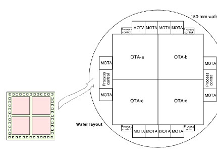
A small, evaluation version of the OTA is called a mini-OTA (MOTA) and consist of a
22 arrays of
OTCCD cells, shown schematically in Figure 1. This MOTA was
included in the wafer layout and has advanced control features of future interest.
Inclusion of MOTA structures allows the novel nature of the OTCCD devices
to be explored while respecting
the compressed schedule for device deliveries [6], [7].
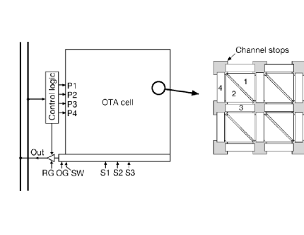
MOTAs provide the opportunity to try advanced features, such as two-phase serial registers, dual output gates and higher performance designs. Each cell has an associated control-logic block, as shown in Fig. 2. The logic block accepts 3 data bits (D2-D1-D0) as inputs and outputs 3 logic levels (Z2-Z1-Z0) to control the parallel clock waveforms applied to each cell (with Z0 and Z1) and to gate the output of the amplifier onto the video column bus OUTn (with signal Z2).The parallel clock voltages applied to each cell are set by four active clock levels, P1A-P4A, and to standby voltages, PSH and PSL, all from off-chip circuitry.
3 CID High Voltage Chip
The CMOS Interface Device for High Voltage version 0 (CID0) is a microelectronic chip
that has been developed using the 0.35m High Voltage process from
AustriaMicroSystems. The main purpose of this chip is to provide the appropiate
voltage signal levels from the STARGRASP111http://www.stargrasp.org/ [5] readout and
control system to the MOTA chip [2, 3, 4].
CID0 also
has additional signals for output monitoring. Some additional test structures
have been included in order to evaluate future additions for a next version of the chip.
The main structures of this chip are visible in Fig. 3.
Table 1 lists the input and
output signals and Table 2 the voltage level requirements.
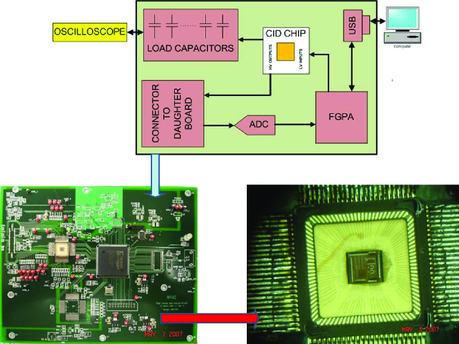
The external layout dimensions are 3262 x 3218 (see Fig. 4 to
see a photograh of the chip at the package). Minimum
pad pitch is 123.
| Output | Pin | VDD | VSS | Ref. | Ref. |
|---|---|---|---|---|---|
| Name | Level | Level | |||
| 1 | RSEL1 | VDD_HV1 | VSS_HV1 | VDDL | LREF |
| 2 | RSEL0 | VDD_HV1 | VSS_HV1 | VDDL | LREF |
| 3 | SW | VDD_HV2 | VSS_HV2 | VDDS | LREF |
| 4 | S3 | VDD_HV2 | VSS_HV2 | VDDS | LREF |
| 5 | S2 | VDD_HV2 | VSS_HV2 | VDDS | LREF |
| 6 | S1 | VDD_HV2 | VSS_HV2 | VDDS | LREF |
| 7 | P4A | VDD_HV3 | VSS_HV3 | VDDH | LREF |
| 8 | P3A | VDD_HV3 | VSS_HV3 | VDDH | LREF |
| 9 | P2A | VDD_HV3 | VSS_HV3 | VDDH | LREF |
| 10 | P1A | VDD_HV3 | VSS_HV3 | VDDH | LREF |
| 11 | PSH | VDD_HV3 | VSS_HV3 | VDDH | LREF |
| 12 | PSL | VDD_HV3 | VSS_HV3 | VDDH | LREF |
| 13 | RG | VDD_HV4 | VSS_HV4 | VDDG | LREF |
| 14 | CSEL1 | VDD_HV1 | VSS_HV1 | VDDL | LREF |
| 15 | D2 | VDD_HV1 | VSS_HV1 | VDDL | LREF |
| 16 | D1 | VDD_HV1 | VSS_HV1 | VDDL | LREF |
| 17 | D0 | VDD_HV1 | VSS_HV1 | VDDL | LREF |
| 18 | CSEL4 | VDD_HV1 | VSS_HV1 | VDDL | LREF |
. Pins Typ.(V) Min.(V) Max.(V) 2 VDD 3.3 3.3 4 2 VSS 0 0 -0.4 2 VDD_HV1 LREF+7 5 8 2 VSS_HV1 LREF -2 -10 2 VDD_HV2 10 5 16 2 VSS_HV2 -6 -3 -10 2 VDD_HV3 LREF+9 7 15 2 VSS_HV3 LREF+1 -1 -10 2 VDD_HV4 10 5 16 2 VSS_HV4 -5 -3 -10
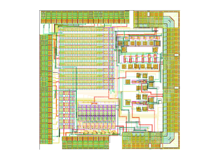
Three main circuit elements included in CID0 occupy different areas of the floorplan and use the following areas: the Level Shifting Subsection of 13901470m for the high current drive circuit and 432940m for the low current drive circuit, Monitor Output Signals area of 945755 and Testing Structures is 10202050.
3.1 Level Shifting Signal Subsection
The level shifting circuitry occupies most of the layout.
In all cases, the input signal is a digital signal with input voltage
levels from 0-3.3V. The output signal corresponds to the input, but with shifted
levels and increased drive strength. There are 2
different capacitive load configurations, 50pF and
1000pF, and in both cases the circuit has to be able to drive up to 25mA. For either
case, the rise time is required to be 100ns.
A 3-stage topology has been adopted: a pre-amplifier
that takes the signals from an initial 0-3.3V and translates
to -3.3V to 16.7V, and a 2-stage output buffer, as indicated
in Fig. 5.
In both cases (high or low load capacitance) the pre-amplifier and the 1st level
output buffer are equal. The 2nd level buffer determines the final strength of
the signal. The voltage levels to which the
various outputs are set are summarized in
Table 1 and Table 2.
3.1.1 Architecture used for the Level Shift Subsection
The architecture developed for the Level Shift Subsection consists of 3 different parts, as seen in Fig. 5.
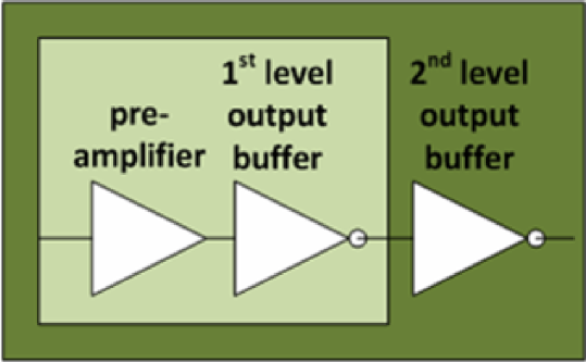
The pre-amplifier and the 1st level buffer convert the signal to the voltage levels needed at every Voltage Output rail. The pre-amplifier is a basic input-differential comparator that converts a low-voltage TTL signal to the extended maximum level (-3.3V, 16.7V). The 1st level buffer shrinks the signal as defined in Table 2, and uses a group of 3 inverters that are used as buffers. The size of these transistors are small, using =40/5 and =40/2.5. The third and last stage is a 2nd level buffer, which determines the final strength of the output signal drive. It consists of 1 inverter, with 2 different sizes, depending on the required output drive strength needed. For loads of 50pF a is used, and for loads of 1000pF a is used.
3.1.2 Waveforms obtained
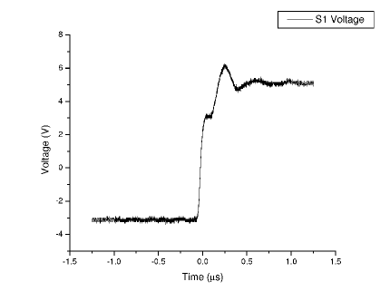
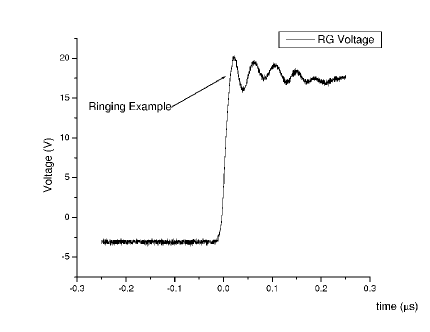
The output waveforms observed in the measurements show ringing coming from the bonding wire inductance. Fig. 6 is a sample Output Voltage for the HV2 rail case. This signal (S1) is driving a load capacitance of 300pF. Fig. 7 correspond to another example of the ringing observed for the RG signal in the case the output voltage is at HV4 levels and a load capacitor with value of 51pF is used.
3.1.3 Rise and Fall Time Measurements
Rise and Fall time measurements have been performed for voltages HV1-HV4, and these transitions times are shown in Fig. 8-11, respectively. These figures show the results of the transition times observed for a specific range of load capacitances, corresponding to the expected MOTA load condition for those signal lines.
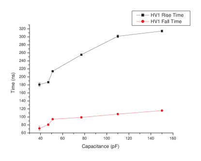
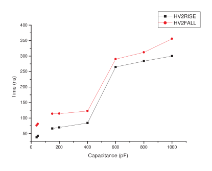
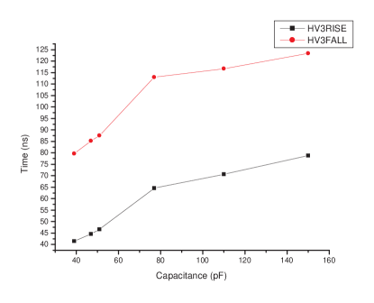
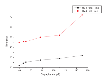
Expected load values for signals of the HV1 are 50pF. The rise and fall times are slightly larger than expected, with rise times that are for the expected output load capacitance. Typical capacitance load values for output banks HV2, HV3 and HV4 are 1000pF. The measurements are again longer and higher than had been hoped. The primary reason is that the maximum drive strength obtained for the pads in this process corresponds to only 24 mA. This value gives a theoretical rise/fall time value for the 1000pF load that is about 3 times the desired value (100ns). The highest values found in Fig. 8 are 300ns for the rise time and 350ns for the fall time.
3.2 Testing Structures
To evaluate future architectures for inclusion of a possible ADC in the next CID version, 3 different testing structures have been included in this chip.
3.2.1 ADC Ramp circuit
The simple structure shown in Figure 12 has been included, where six different values for the capacitors have been used (from 0.80pF to 3.12pF). The capacitor used is Cpoly, formed from poly1 and poly2.
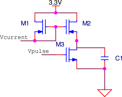
In all configurations the Cramp gets dominated by oscilloscope capacitance (12pF), with V=3.3V and t=2.8ms, showing the current is higher than initially simulated (2.55mA vs 1.0mA)
3.2.2 ADC Comparator Testing

This structure includes the previous structure and a comparator. The comparator is a voltage comparator with a preamplification stage, a decision circuit stage and an output buffer that works at 1MHz. Fig. 13 shows a general schematic that includes the ramp generator that is also present in this configuration.
3.2.3 Sample and Hold Testing
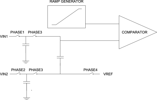
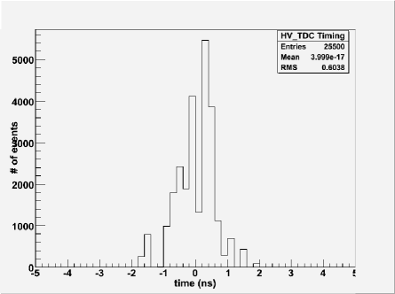
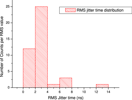
In this structure a differential storage of the value is done and then shifted using a reference value. This value is then used for the comparison with the ramp signal, the comparator output of which time encodes the analog value. Fig. 14 ilustrates the general architecture. To test this structure, an FPGA-based TDC has been used [1], with a 2ns time step and a measured time resolution of 0.604ns, as plotted in Fig. 15. The measured transfer curve is displated in Fig. 16. Noise coming from the jitter of the FPGA has been substracted from the total RMS noise, see Fig. 17, according to Eq. 1. Fig. 18 shows the residual errors obtained in the voltage determination.
| (1) |
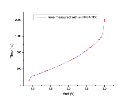
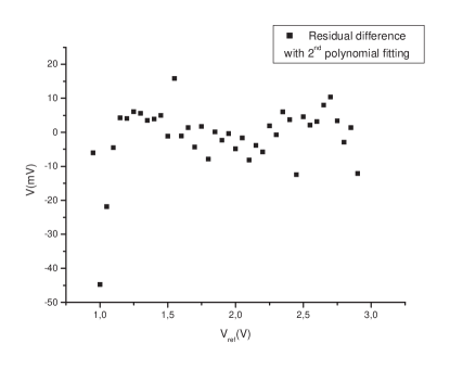
A fitting of the distribution has been done using a second order polynomial, with Time = A + B1 Vref + B2 Vref2, with weights given by the error bars. The fitting parameters obtained are A = 160.75 40.56 ns, B1 = -38.78 45.45 ns/V, B2 = 163.83 11.95 ns/V2. The correlation coefficient value is r=0.9955, which promises good performance of the system.
4 Conclusion
MOTA CCDs need control signal levels that are much different than those typically available for standard logic and need to span something like -5V to 20V. To provide this level translation the CID0 HV CMOS ASIC has been fabricated and tested. This chip has been used to evaluate the 0.35m HV process from AustriaMicrosystems. The CID0 chip includes the level shifting circuitry needed for MOTA interfacing, as well as some additional testing structures. The High Voltage Chip is interfaced to the CCD using a Flex connector during the test of the prototype. The final goal of this project is to integrate in the same substrate the CCD and the chip, this approach will also prevent any more ringing problems coming from the inductance at the bonding wires used in this version. Observed level shift circuitry performance matches expectations for this process, although the drive strength of the pads used here is not sufficient for a final 10MHz operation. In order to meet the design requirements there is an option that has been analyzed. This option is to develop our own pads, which will show a suitable drive strength value, for the time being the CID0 chip will be used with the actual performance. Wilkinson ADC test structures have been evaluated and show promise for implementing complex readout structures in close proximity and at the high voltage levels typical of OTCCD devices.
Acknowledgements.
The authors thank the Vice Chancellor for Research of the University of Hawaii for his support of this project.References
- [1] G. Varner, The Modern FPGA as Discriminator, TDC and ADC, \jinst12006P07001.
- [2] B. Burke, An Orthogonal-Transfer CCD Imager, Rev. IEEE Trans. Elec. Dev., 41 (1994) 12 2482-2484.
- [3] D. Smith et al, Development and Testing of a 2-D Transfar CCD, IEEE Trans. Elec. Dev., 53 (2006) 11 (2748-2754).
- [4] S. Howell et al, Photometric Observations Using Orthogonal Transfer CCDs, Publications of the Astronomical Society of the Pacific, 115 (2003) 1340-1350.
- [5] S. Keller et al, The SkyMapper Telescope and The Southern Sky Survey, Publications of the Astronomical Society of Australia , 24 (2007) 1-12.
- [6] B. Burke et al, Development of the orthogonal-transfer array, in Sensors, Cameras and Systems for Scientific/Industrial Applications VII, 173-180, SPIE, 2006.
- [7] B. Burke et al, The orthogonal-transfer array: a new CCD architecture for astronomy, in Optical and Infrared Detectors for Astronomy, 185-192, SPIE, 2004
- [8] K. Hodapp, Design of the Pan-STARRS telescopes, Astron. Nachr., 325 (2004) 636-642.
- [9] N. Kaiser, Pan-STARRS: a wide-field optical survey telescope array, Proceedings of SPI - Ground-based Telescopes, 5489 (2004) 11-22.