Tunable spin-gaps in a quantum-confined geometry
Abstract
We have studied the interplay of a giant spin-orbit splitting and of quantum confinement in artificial Bi-Ag-Si trilayer structures. Angle-resolved photoelectron spectroscopy (ARPES) reveals the formation of a complex spin-dependent gap structure, which can be tuned by varying the thickness of the Ag buffer layer. This provides a means to tailor the electronic structure at the Fermi energy, with potential applications for silicon-compatible spintronic devices.
pacs:
73.20.At, 73.21.Fg, 79.60.Jv, 79.60.Bm, 71.70.EjIn nonmagnetic centrosymmetric bulk solids like silicon, electronic states of opposite spin have the same energy. A surface or an interface breaks the translational invariance of a three-dimensional crystal. Thus, as predicted by Bychkov and RashbaBychkov and Rashba (1984), the spin-orbit (SO) interaction can lead to spin-split electronic states in two-dimensional electron gases (2DEG), in asymmetric quantum wellsKoga et al. (2002), at a surface or at an interfaceLaShell et al. (1996); Rotenberg et al. (1999). The size of the splitting is related to the strength of the atomic SO coupling (i. e. to the gradient of the atomic potentialMalterre et al. (2007)) and to the potential gradient perpendicular to the confinementForster et al. (2004). An unexpectedly large splitting was recently reported for a BiAg surface alloy grown on a Ag(111) single crystalAst et al. (2007). It is attributed to an additional in-plane gradient of the surface potential, hence being a direct consequence of the chemical alloy configurationAst et al. (2007); Premper et al. (2007).
The spin-orbit interaction could be used to control via a gate voltage the dynamics of spins injected into a semiconductorDatta and Das (1990); Awshalom and Flaté (2007); Koga et al. (2002); Nitta et al. (1997). Moreover, the spin Hall effect - also induced by the SO interaction - could find applications in new spintronic devicesKato et al. (2004); Valenzuela and Tinkham (2006) which rely neither on magnetic materials nor on optical pumping. Interfaces between silicon and materials exhibiting large spin-orbit splitting are therefore expected to open novel vista for spintronics. The challenge is to control the electronic states and spin polarization at the Fermi level which determine the electron and spin transport through interfacesGreullet et al. (2007); Tsymbal et al. (2007) and nanostructures. Among the heavy metals which exhibit strong spin-orbit interactions, bismuth may be favored for environmental considerations. Experiments on thin layers of bismuth on silicon have evidenced a SO splitting in the Bi surface states, but not of their bulk counterparts Hirahara et al. (2006, 2007). Moreover, it was observed that the splitting is removed by the hybridization between surface and bulk states.
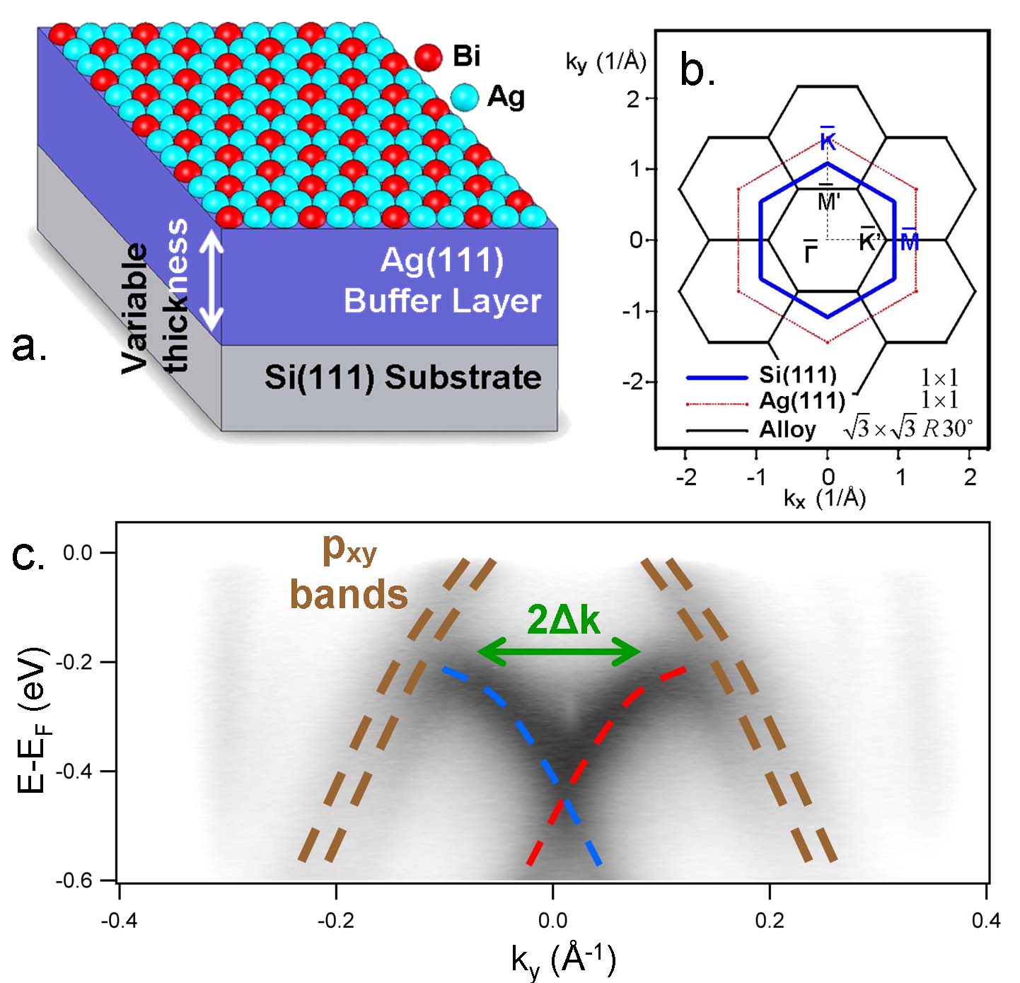
In this Letter we explore a different approach. We fabricated trilayer systems composed of a BiAg surface alloyAst et al. (2007), a thin Ag buffer layer of variable thickness (d), and a Si(111) substrate (Fig. 1a). Along the z direction, the vacuum/BiAg/Ag/Si related potential is asymmetric and SO splitting of delocalized electronic states is expected. The good interfacial adhesion of the silver film makes the system stable at room temperature (RT) and results in a sharp interface. We investigated the complex interface by angle-resolved photoelectron spectroscopy (ARPES) experiment, supported by first-principles electronic-structure calculations. We find that the SO splitting is large. We also find that, due to quantum confinement in the buffer layer, the electronic structure exhibits patches of highly spin-polarized spectral density. The spin-dependent density of states close to the Fermi energy can be tuned by the thickness of the Ag buffer.
The experiments were performed with a multi-chamber set-up under ultra-high vacuum. During preparation, Si(111) (highly phosphorus doped, resistivity 0.009 - 0.011) was flashed at 1200∘C by direct current injection. After the flashes, the substrate was cooled slowly in order to obtain a sharp 7 7 signature in low-energy electron diffraction (LEED). The Ag films were deposited with a home made Knudsen cell while the sample was kept at 80K and then annealed at 400K. The quality of the silver thin film was checked by LEED. Ag grows in the [111] direction Speer et al. (2006). The BiAg surface alloy was obtained by depositing 1/3ML of Bi with an EFM3 Omicron source on the sample at RT followed by a soft annealing. Angle-resolved photoemission spectroscopy (ARPES) spectra were acquired at RT and 55K with a PHOIBOS 150 Specs Analyser. We used a monochromatized and partially polarized GammaData VUV 5000 high brightness source of 21.2eV photons.
The first-principles electronic-structure calculations are based on the local spin-density approximation to density functional theory, as implemented in relativistic multiple-scattering theory (Korringa-Kohn-Rostoker and layer-Korringa-Kohn-Rostoker methods; for details, see refs. Ast et al. (2007, 2008)). Spin-orbit coupling is taken into account by solving the Dirac equation. The used computer codes consider the boundary conditions present in experiment, that is the semi-infinite substrate, a buffer of finite thickness, the surface, and the semi-infinite vacuum. The potentials of all sites (atoms) are computed self-consistently, except for the Si substrate which is mimicked by spherical repulsive potentials of 1 Hartree height. This so-called hard-sphere substrate follows the face-centered cubic structure of the Ag buffer. The electronic structure is addressed in terms of the spectral density which is obtained from the imaginary part of the Green function of the entire system. The latter can be resolved with respect to wavevector, site, spin and angular momentum, thus allowing a detailed analysis of the local electronic structure.
The surface electronic properties of the alloy grown on top of a thick Ag film (d=80 monolayers (ML)), as obtained by ARPES (Fig. 1c), agree with those of the alloy grown on a Ag(111) single crystalAst et al. (2007). The spin-split bands which belong to electronic states with spz character cross at (in-plane wavevector ). They are well described by parabolas (effective mass m* = -0.35 me) which are offset by Å-1. This shift in wavevector is a signature of the aforementioned Rashba effect. The set of side bands stems from electronic states of mainly pxpy character which are also spin-polarized but less splitAst et al. (2007); Premper et al. (2007); Meier et al. (2008). Electronic-structure calculationsAst et al. (2007) show that the BiAg surface states are much more strongly localized in the top layer than the Ag(111) or Au(111) Shockley surface states. Thus, the spin-split bands and the giant SO splitting are not directly affected by the Ag/Si interface for Ag film thickness larger than a few monolayers. This implies that prior results for BiAg/Ag(111)Ast et al. (2007) can be transferred to silicon technology (i.e. to BiAg/Ag/Si(111)) at RT.
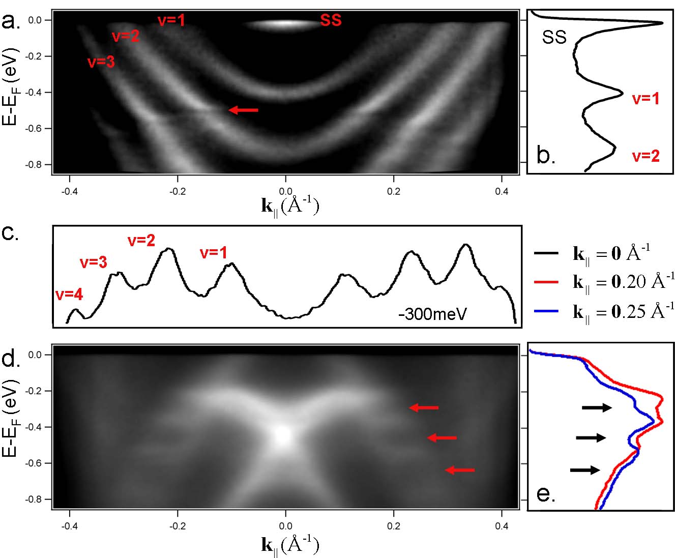
A new and interesting situation arises for thinner Ag buffer layers, where d is of the order of the attenuation length of the electronic states. The Ag sp states are confined to the Ag film by the potential barrier (image-potential barrier) on the vacuum side (surface) and by the fundamental band gap of Si on the substrate side. This confinement leads to quantized wavevectors along z and to discrete energy levelsChiang (2000). These so-called quantum well states (QWS’s) play a central role in transport propertiesJalochowski et al. (1992) and in the coupling of magnetic layers in superlatticesOrtega and Himpsel (1992); Ortega et al. (1993); Bruno (1995). Ag/Si(111) QWS’s, in particular, have been extensively studied by ARPESSpeer et al. (2006); Wachs et al. (1986); Sanchez-Royo et al. (2002). For Ag(111) films, their in-plane dispersion consists of a set of parabolic bands centered at , with energies determined by the film thickness (Fig. 2a; d=17 ML). The electronic fringe structure with a negative parabolic dispersion appears due to the accumulation of QWS’s near the k-dependent valence band edge of Si. This is an indirect manifestation of the heavily-doped n-type character of the Si(111) substrates used hereSpeer et al. (2006). The narrow lineshapes of the energy distribution curves (EDC’s; Fig. 2b) and momentum distribution curves (MDC’s; Fig. 2c), and the observations of the electronic fringes reflect the uniformity of the Ag buffers and the high resolution of the experiment.
Having discussed the spin-split BiAg surface states and the quantum-well states in the Ag buffer (without BiAg surface alloy), we consider their interaction in a BiAg/Ag/Si trilayer, focusing first on a 17 ML thick Ag buffer (Fig. 2d; i.e. the sample of Fig. 2a covered by the BiAg alloy). The Ag Shockley surface state disappears and the resulting surface electronic structure agrees in general with that of the system without Si substrate (BiAg/Ag(111); no QWS’s) but shows intensity modulations in both the spz and pxpy bands. The energy distribution curves, extracted from the raw data, clearly evidence band gaps (Fig. 2e).
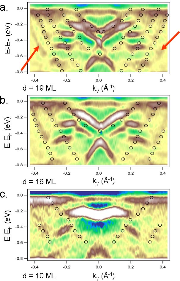
The remaining signature of the Ag QWS’s (at large k values) and the gaps in BiAg surface states are clearly seen even at RT in the second derivative of the ARPES intensities () for samples with selected Ag film thicknesses (d = 19, 16, and 10ML) in Fig. 3. The parabolic in-plane dispersions of the QWS’s (circles in Fig. 3) is obtained from MDC’s of Ag/Si(111) with the corresponding Ag thicknesses (as presented in Fig. 2c). Agreement between the parabolic fits (uncovered Ag buffer) and the QWS’s of the alloyed sample is obtained after shifting rigidly the parabola by meV to lower binding energies. These shifts can be attributed to the different reflection properties of the bare Ag surface and of the BiAg surface alloy or to a possible reorganization of the thin film upon Bi deposition. The effective masses of the QWS’s may also change. Yet, these fits are to be considered as guides to the eye. Band gaps are found at the intersection of the QWS fits with both branches of the surface-alloy bands regardless of their symmetry or spin, providing strong evidence of their hybridization. The hybridization is spin-selectiveDidiot et al. (2006); Barke et al. (2006) thus we can consider in a first approximation that the QWS are spin-degenerate or their spin-splitting is small. For thinner Ag buffers (10ML; Fig. 3c), the number of QWS’s is reduced. As a result, the number of band gaps is also decreased but their widths are larger, in particular for the pxpy states.
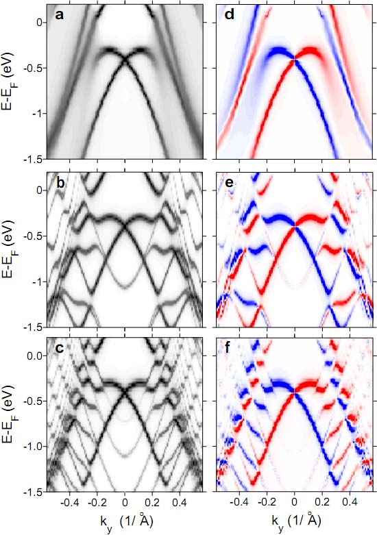
To further corroborate the above explanation of the band gaps, first-principles electronic structure calculations for BiAg/Ag(111) reported inAst et al. (2007, 2008) were extended. Since the Ag/Si(111) interface is incommensurateSpeer et al. (2006), we are forced to approximate the Si substrate. Therefore, the confinement of the Ag QWS’s by the Si(111) substrate is mimicked by replacing Ag bulk layers by repulsive potentials. The latter provide the complete reflection of the Ag states at the Ag/Si(111) interface. Note that by this means details of the Ag/Si interface are roughly approximated and the binding energies of the theoretical quantum well states may differ from their experimental counterparts. However, the essential features are fully captured, as will be clear from the agreement of experiment and theory discussed below. The systems investigated comprise the BiAg surface alloy, Ag layers, and the substrate built from hard spheres (HS; i. e. BiAg/Agd-1/HS(111)). The theoretical analysis focuses on the wavevector- and spin-resolved spectral density at a Bi site (or is the spin quantum number). Spin-dependent band gaps are conveniently visualized by displaying .
For BiAg/Ag(111), the Bi surface states hybridize with Ag bulk states, resulting in a rather blurred spectral density (Fig. 4a; compare Fig. 1c for the experiment). For the systems with Si substrate, focusing here on exemplary results for d = 10 (Fig. 4b) and 19 (Fig. 4c), quantum well states show up as parabolas centered at . The most striking difference to BiAg/Ag(111) are, however, spin-dependent band gaps at points at which the QWS’s would cross the Bi bands. With increasing thickness of the Ag buffer, the number of gaps (or QWS’s) increases and the width of the gaps decreases. The spectral densities of the Bi states are slightly less blurred than for BiAg/Ag(111) because hybridization with Ag states occurs only at the band gaps, due to quantization. Eventually, we find a shift of the QWSs’ energies upon covering the Ag buffer with the BiAg alloy, in agreement with experiment. In summary, the electronic-structure calculations corroborate fully the experimental findings.
By contrast with what has been observed in Bi thin layers on siliconHirahara et al. (2006, 2007), Figs. 4e and f clearly show that the Ag quantum well states are spin-polarized due to the Rashba effect. Close to , the branches of opposite spins of the QWS follow a parabolic dispersion and their momentum separation decreases with the Ag thickness. This feature is evident in figures that show spin polarization of the electron states, . We now address in particular the electronic structure at the Fermi level. For d=10ML (Fig. 4e), highly spin-polarized states show up at Å-1, with a spin polarization of about 33%. On the contrary, a complete gap appears for d=19 ML (Fig. 4f). These findings imply that the spin-dependent electronic structure at the Fermi level - and thus the transport properties - can be drastically modified by the Ag film thickness.
Our findings for BiAg/Ag/Si(111) trilayers suggest that it is indeed possible to match systems with large spin-orbit splitting (here: BiAg/Ag(111)) with a semiconductor substrate. Furthermore, interfacial properties can be custom-tailored, in the present case by a single parameter, namely the Ag buffer layer thickness. Within this respect, multilayer systems which comprise semiconducting Si layers and Rashba-split subsystems (like BiAg/Ag) may be very useful in the development of new spintronics devices. Tuning the band-gap structure at the Fermi level could also be achieved by chemical means, as was demonstrated for BixPb1-xAg2 mixed alloys grown on Ag(111)Ast et al. (2008). Peculiar transport properties and spin Hall effects can be anticipated based on this interface, namely in nanostructured systems or (Bi-Ag-Si) superlattices.
Acknowledgements.
E.F. acknowledges the Alexander S. Onassis Public Benefit Foundation for the award of a scholarship. This research was supported in part by the Swiss NSF and the NCCR MaNEP.References
- Bychkov and Rashba (1984) Y. Bychkov and E. Rashba, JETP Lett. 39, 78 (1984).
- Koga et al. (2002) T. Koga et al., Phys. Rev. Lett. 88, 126601 (2002).
- LaShell et al. (1996) S. LaShell, B. McDougall, and E. Jensen, Phys. Rev. Lett. 77, 3419 (1996).
- Rotenberg et al. (1999) E. Rotenberg, J.W. Chung, and S. Kevan, Phys. Rev. Lett. 82, 4066 (1999).
- Malterre et al. (2007) D. Malterre et al., New J. Phys. 9, 391 (2007).
- Forster et al. (2004) F. Forster, S. Hüfner, and F. Reinert, J. Phys. Chem. B 108, 14692 (2004).
- Ast et al. (2007) C. R. Ast et al., Phys. Rev. Lett. 98, 186807 (2007).
- Premper et al. (2007) J. Premper et al., Phys. Rev. B 76, 073310 (2007).
- Datta and Das (1990) S. Datta and B. Das, Appl. Phys. Lett. 56, 665 (1990).
- Awshalom and Flaté (2007) D. Awshalom and M. Flaté, Nature Phys. 3, 153 (2007).
- Nitta et al. (1997) J. Nitta et al., Phys. Rev. Lett. 78, 1335 (1997).
- Kato et al. (2004) Y. Kato et al., Nature 427, 50 (2004).
- Valenzuela and Tinkham (2006) S. Valenzuela and M. Tinkham, Nature 442, 176 (2006).
- Greullet et al. (2007) F. Greullet et al., Phys. Rev. Lett. 99, 187202 (2007).
- Tsymbal et al. (2007) E. Tsymbal et al., Prog. Mater. Sci. 52, 401 (2007).
- Hirahara et al. (2006) T. Hirahara et al., Phys. Rev. Lett. 97, 146803 (2006).
- Hirahara et al. (2007) T. Hirahara et al., Phys. Rev. B 76, 153305 (2007).
- Speer et al. (2006) N. Speer, S. Tan, and T.-C. Chiang, Science 314, 804 (2006).
- Ast et al. (2008) C. R. Ast et al., Phys. Rev. B 77, 081407(R) (2008).
- Meier et al. (2008) F. Meier et al., Phys. Rev. B 77, 165431(2008).
- Chiang (2000) T.-C. Chiang, Surf. Sci. Rep. 39, 181 (2000).
- Jalochowski et al. (1992) M. Jalochowski et al., Phys. Rev. B 45, 13607 (1992).
- Ortega and Himpsel (1992) J. E. Ortega and F. J. Himpsel, Phys. Rev. Lett. 69, 844 (1992).
- Ortega et al. (1993) J. Ortega et al., Phys. Rev. B 47, 1540 (1993).
- Bruno (1995) P. Bruno, Phys. Rev. B 52, 411 (1995).
- Wachs et al. (1986) A. L. Wachs et al., Phys. Rev. B 33, 1460 (1986).
- Sanchez-Royo et al. (2002) J. F. Sanchez-Royo et al., Phys. Rev. B 66, 035401 (2002).
- Didiot et al. (2006) C. Didiot et al., Phys. Rev. B 74, 081404(R) (2006).
- Barke et al. (2006) I. Barke et al., Phys. Rev. Lett. 97, 226405 (2006).