Characterisation of nanostructured GaSb : Comparison between large-area optical and local direct microscopic techniques
Abstract
Low energy ion-beam sputtering of GaSb results in self-organized nanostructures, with the potential of structuring large surface areas. Characterisation of such nanostructures by optical methods is studied and compared to direct (local) microscopic methods. The samples consist of densely packed GaSb cones on bulk GaSb, approximately , and in height, prepared by sputtering at normal incidence. The optical properties are studied by spectroscopic ellipsometry, in the range –, and with Mueller matrix ellipsometry in the visible range, –. The optical measurements are compared to direct topography measurements obtained by Scanning Electron Microscopy (SEM), High Resolution Transmission Electron Microscopy (HR-TEM), and Atomic Force Microscopy (AFM). Good agreement is achieved between the two classes of methods when the experimental optical response of the short cones () is inverted with respect to topological surface information via a graded anisotropic effective medium model. The main topological parameter measured was the average cone height, but estimates of typical cone shape and density (in terms of volume fractions) were also obtained. The graded anisotropic effective medium model treats the cones as a stack of concentric cylinders (discs) of non-increasing radii. The longer cones ( ) were found experimentally to give rise to considerable reduction in the measured degree of polarisation. This is presumably caused by multiple scattering effects, and thereby questions in this case the validity of the effective medium approximation. Moreover, the reflectance of the samples were also measured and modelled, and found to be reduced significantly due to the nano-structuration. Optical methods are shown to represent a valuable characterization tool of nanostructured surfaces, in particular when large coverage area is desirable. Due to the fast and non-destructive properties of optical techniques, they may readily be adapted to in-situ configurations.
1 Introduction
The recent advent of nano-technology and nano-science has made it increasingly important to be able “see” features of a sample down to a nanometric scale. This is today typically achieved with the aid of several well-established microscopic techniques like, Atomic Force Microscopy (AFM), Scanning Electron Microscopy (SEM) and Transmission Electron Microscopy (TEM). All these techniques can achieve nanometric resolution, and are therefore attractive when one wants to image the fine details of a sample. Moreover, they can be said to be local in the sense that only a rather small surface area can be imaged with good resolution. They are also rather time consuming techniques, and the required equipment is costly and physically large. As a result, they are not generally suited for in-situ characterisation.
Traditionally, optical techniques have been attractive for in-situ studies due to its measurement speed, relatively low equipment cost, non-contact properties and ease of integration with other setups. Optical techniques also have the advantage of being able to cover large surface area with relative ease. This is a great advantage, for instance, in monitoring applications where it is the average properties that are of interest, and not the local features at a given location at the surface. For nanometre scale structures, the applicability of optical techniques are limited by the diffraction limit [1], making imaging of such structures by visible light impossible. However, even if direct optical imaging is challenging for nano-structures, it is well-known that they can have strong polarisation altering properties on the incident radiation. Hence, indirect optical techniques can in principle be devised for the purpose of extracting topographic information about the sample. The aim of this paper is to present such a methodology, and to compare the large area optical result to local information obtained by direct methods.
Spectroscopic ellipsometry (SE) is a celebrated polarimetric technique, much used for measuring the thickness of thin film layers, and for determining the index of refraction of materials. It can also be used to characterise nanostructures. For example, generalised ellipsometry has been used to measure the inclination angle of nano-rods [2]. The sensitivity of spectroscopic ellipsometry to the thickness of thin layers is remarkable, and can be down to single atom layers. This is achieved by knowing the refractive indices of the materials, and utilising optical models. The aim of this study is to exploit SE’s sensitivity of thin film thickness, in order to accurately measure the height of conical shaped nanostructures. This is done by developing a suitable optical model. Information on shape and regularity can also possibly be attained. The ellipsometric spot will always average over a relatively large (surface) area, providing information on the mean properties of the structures. It is both non-invasive and fast, making it suitable as a tool for in-situ characterisation.
Nanostructured surfaces and materials open up for a new range of applications. In photonics, for example, optical properties of thin films may be mimicked by nanostructures, and further supply new and enhanced properties (see e.g. [2], and references therein). An example of such properties can be anti-reflective coatings with low reflectivity over a large spectral range and a wide range of incident angles [3].
Low energy ion sputtered GaSb is a good example of self-organized formation of densely packed cones, and has been proposed as a cost-effective method for production of e.g. quantum dots [4]. The properties of such a surface may, to a large extent, be tailored by controlling sputtering conditions. The latter issue is a typical target application area of ellipsometry. In the case of a future large scale production of such surfaces, SE could possibly be used as an efficient production control tool for testing individual samples.
Here, optical models are initially constructed from observations from High Resolution Transmission Electron Microscopy (HR-TEM), Field Emission Gun Scanning Electron Microscopy (FEG-SEM), and AFM. The latter give a direct observation of the nanostructures, with respect to density, cone separation, cone height, number of nearest neighbours etc. Information on the shape and crystal structure of individual cones, were obtained from HR-TEM studies of carefully prepared slices of nanostructured GaSb.
This paper is organized as follows: In section 2 we describe the experimental details of both the direct microscopic (SEM, TEM and AFM), and the optical (SE) studies. A brief theoretical background on ellipsometry is also given. In section 3 we present the results of these studies. The optical properties of conical nanostructures are discussed in relation to the effective medium approximation. An optical model is presented in section 3.3, that enables characterisation of such structures from optical measurements, by fitting the model parameters to the SE measurements.Information gained from the optical characterisation are finally compared to the results from the direct microscopic studies.
2 Experimental details and theoretical background
The samples consisted of GaSb sputtered at low-ion-energy [5]. The deposition condition for each sample is reported in table 1. The substrates were crystalline GaSb () wafers, of thickness . All samples were sputtered at room temperature. The FEG-SEM images were obtained using a Hitachi S-4300SE, and Zeiss Supra instruments. TEM analysis was performed using a JEOL 2010F. Cross section TEM samples were prepared by both ion-milling and ultramicrotomy, in order to investigate possible preparation induced artefacts in the microstructure. Ion-milling was performed using a Gatan PIPS instrument, operating at with a thinning angle of –. Ultramicrotomy was performed using a Reichart-Jung Ultracut E instrument. AFM measurements were done by a DI-VEECO AFM with a NanoScope IIIa controller from Digital Instruments, operated in tapping mode. Silicon tips with radius less than were used.
The optical far field measurements were performed using a commercial Photo-Elastic-Modulator Spectroscopic Ellipsometer (PMSE) in the photon energy range – (UVISEL, Horriba Jobin Yvon), at an angle of incidence of . The complete Mueller matrix was also measured using a commercial ferroelectric liquid-crystal retarder-based Mueller matrix Ellipsometer (MM16) in the range – (–). Such measurements where made for several angles of incidence in the range from to , and as a function of the sample rotation angle around its normal to the (mean) surface. The orientation of the sample with respect to the direction of the incoming beam was carefully recorded, and the sample was rotated manually in steps of , with a total sample rotation in all cases of at least .
The PMSE measurements were performed in the standard UVISEL set-up, i.e. polariser-sample-PEM-analyser, where the angle of the fast axis of the PEM with respect to the analyser is fixed at . Measurements were performed in the standard PMSE configurations (, ) [6], determining and , where and are normalised Mueller matrix elements related to the unormalised Mueller matrix by . For the reflection from a isotropic planar surface, they can be defined according to
| (1) |
and
| (2) |
where and denote the ellispometric angles related to the ratio of the complex reflection amplitudes [7].
Additional measurements were performed in the configuration (, ), enabling the determination of
| (3) |
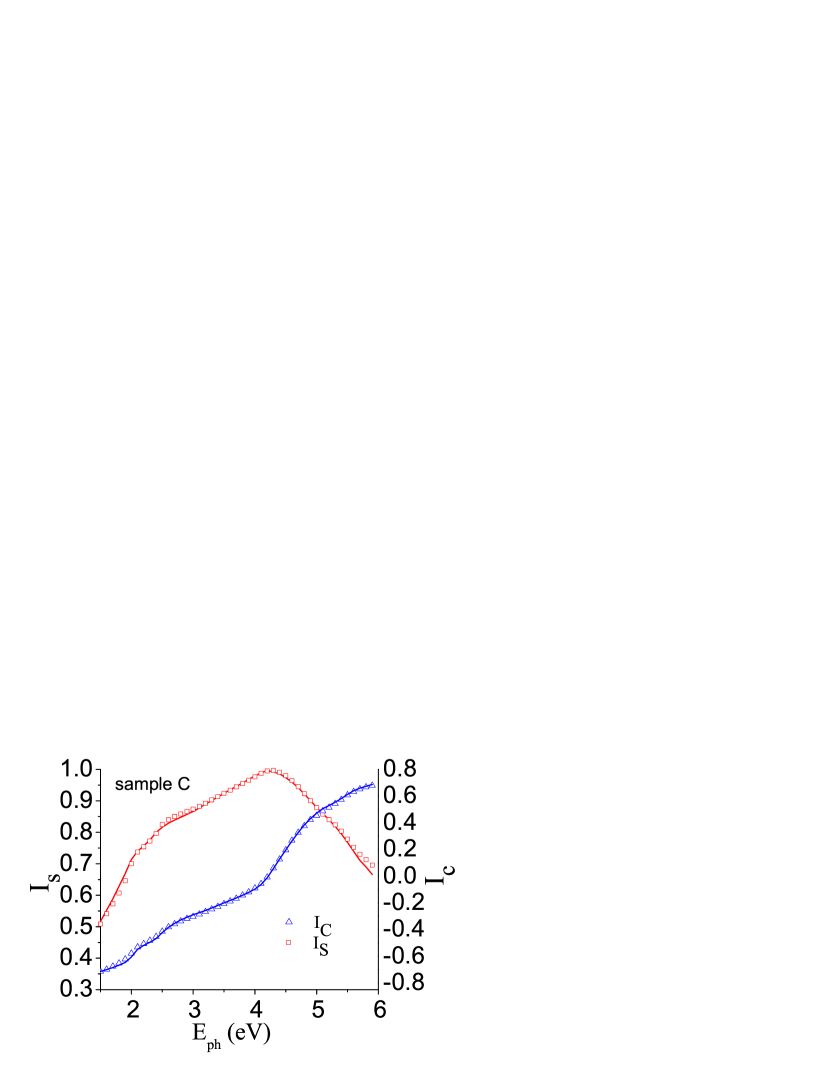
The quantities, , and , as defined in equations (1)–(3) are known as the ellipsometric intensities. For block-diagonal Mueller matrices, these intensities can be used to define the degree of polarisation, . [8]
| (4) |
A discussion on when a sample will have a block-diagonal Mueller matrix will be given in the following section. From the full Mueller matrix, experimentally available here in the range –, it is also customary to define the so-called depolarisation index 111Consult e.g. Ref. [9] for a more detailed discussion of depolarisation measures.
| (5) |
where denotes the non-normalised Mueller matrix elements [9]. (and in most cases ) determine how much of the outgoing light will be totally polarised for totally polarised incident light. ”‘Reflectance measurements”’ were also performed by the PMSE, in which was determined by using a standard Al mirror reference sample, and assuming stable intensity conditions. The reflectance spectrum was recorded from – in steps of .
3 Results and discussion
3.1 Experimental observations — SEM, TEM and AFM results
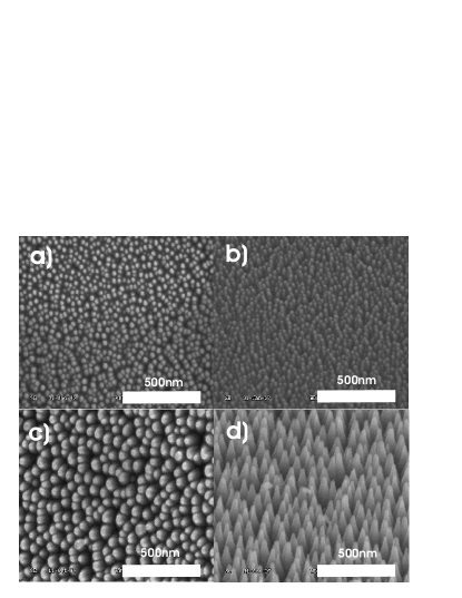
In figure 1, FEG-SEM images of samples and are presented, for both normal beam incidence (left-hand images), and tilted beam incidence (right-hand images). The cones do not show a high degree of organisation, but on average have 6 nearest neighbours. This result was found from statistical treatment of AFM measurements of the samples, but could as well have been found from SEM images. The result correspond well with Euler’s law [10], which state that the mean number of nearest neighbours for a structure created by a random process is . The average cone separation, , has been estimated from the cone density, by assuming the cones to be ordered on a perfect hexagonal lattice. The average height of the cones, , were nominally estimated from AFM, but for sample , it was estimated from HR-TEM. The average cone heights and cone separations are given in table 2, along with the estimated standard deviation of .
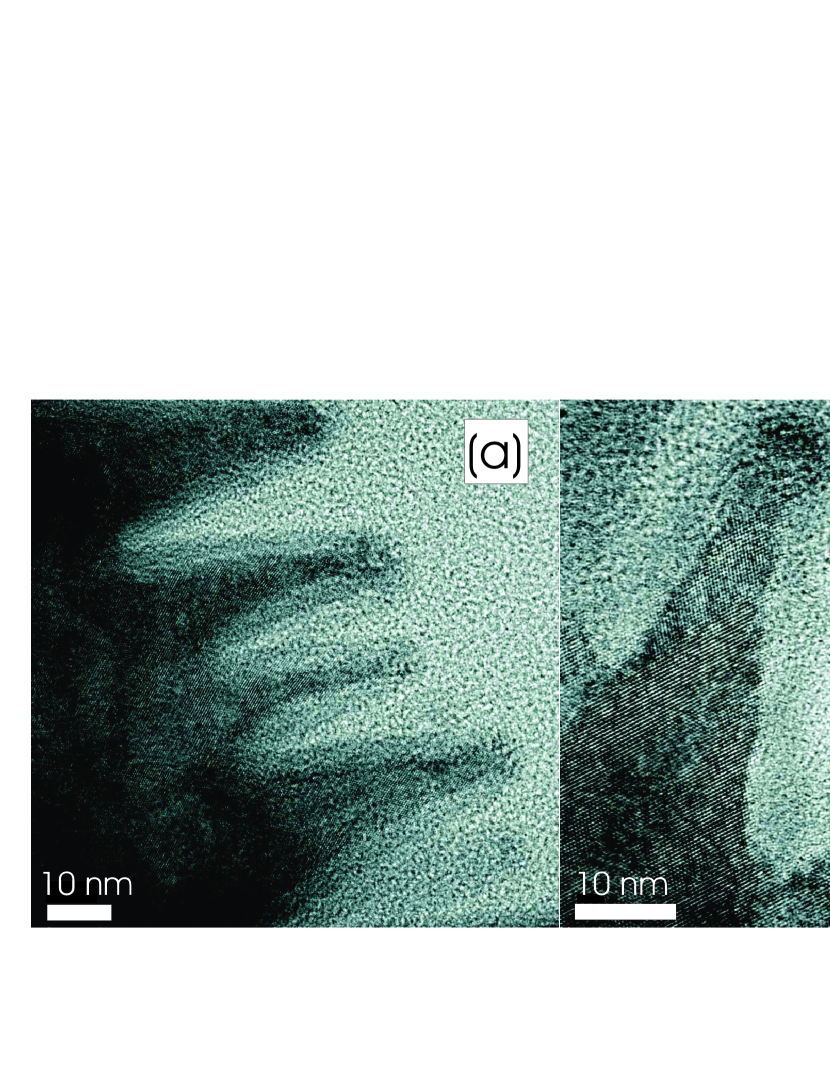
Figure 2 depicts a HR-TEM image of selected cones from sample A, prepared by ion-milling. The average cone height of A was estimated to be , obtained by taking the average of cones measured by HR-TEM. The shape was found to be conical with a somewhat rounded tip. The typical cone angle, defined as the angle between the substrate and the cone side wall, was found to be roughly . From the HR-TEM images in figure 2, it is observed that the interior of the cones consisted of primarily crystalline material, with the same crystal orientation as the substrate. Furthermore, the cone surface appeared to be surrounded by a thin (less than ) layer of undetermined amorphous material. From the rapid oxidation of clean GaSb to an approximately – GaSb-oxide layer, it is argued that this surrounding layer is partially oxidised.
Another slice of nanostructured GaSb (sample ) , was prepared by ultramicrotomy. This sample did not provide such a thin sector as the ion-milled samples. However, it was sufficient to confirm the structure observed in the ion-milled samples. The crystalline nature of the interior of the cones, and the amorphous surrounding layer is in line with the observations by Fascko et al. [4].
In summary, from the TEM studies mainly three phases appear to be involved in the layer (thin film) defined by the cones. These phases are crystalline GaSb (c-GaSb), amorphous GaSb (a-GaSb) and presumed GaSb-oxide, in addition to the voids between the cones. Theremaining samples were studied by AFM and by FEG-SEM, and detailed results are compiled in table 2. It is suspected that the AFM tip is too blunt to reach the bottom between close-packed cones. Therefore, when estimating the average cone height , the height of each cone top have been defined relative to the lowest point in an area within the maximal distance between the cones. This minimum is typically found in a place where the cones stand further apart, and the tip can reach the bottom. This may overestimate the average height somewhat.
3.2 Experimental observations — Spectroscopic Ellipsometry
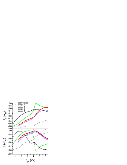
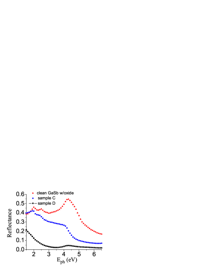
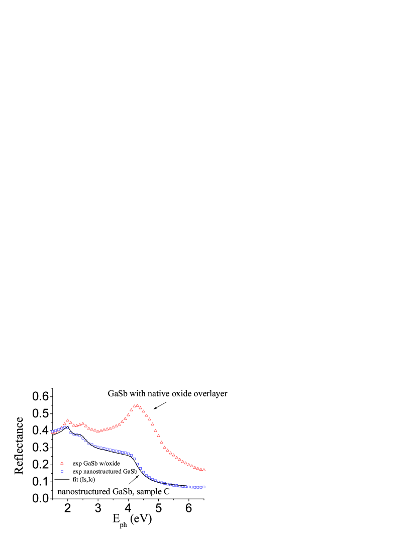
Figure 3 shows the SE measurements of , of a clean Gasb surface with approximately of oxide. In addition it shows, as an overview, the ellipsometric measurements of samples , and (short cones) and (longer cones). All cones were formed by sputtering at normal incidence. The nano-structuration of the surface strongly modifies the polarisation dependent optical response. Another interesting feature is the reflectance of such nanostructured surfaces, which have additional practical applications. It is particularly clear from figure 4 that the reflectance is much reduced, compared to the clean surface, at higher photon energies. Furthermore, the antireflection properties tend to appear for lower energies as the cones get higher. This could be explained as a ”motheye” effect from the graded index of refraction [11].
From FEG-SEM and HR-TEM images, it is observed that the samples consist of conical nanostructures of various sizes. For sufficiently small cones, the surface can be treated as a thin film layer of effective medium. This layer will be uniaxially anisotropic , since the cones will show a different response to an electric field normal to the mean surface, than to a field parallel to it. Anisotropic uniaxial materials with the optic axis in the plane of incidence, will appear like an isotropic material under ellipsometric investigations [12], in the sense that reflections from such materials will be described by a diagonal Jones matrix, and by a block diagonal Mueller-Jones matrix. This means that all the polarisation altering properties of the structured surface can be described by the ellipsometric angles and , derived from the ellipsometric intensities and .
Cones being directed normal to the surface have a symmetry axis that is normal to the mean surface , and the approximated effective media must therefore have an optic axis in the same direction, i.e. it will appear like an isotropic material, and can be fully characterised by regular (standard) ellipsometry. The samples will then have full azimuth rotation symmetry (around the sample normal). If the cones are tilted from the sample normal, this will generally no longer be the case (except for the two special azimuth orientations where the tilted cones lie in the plane of incidence). The structures will then correspond to an anisotropic material with a tilted optic axis. To describe the polarising properties of reflections from such a surface, one also needs to account for the coupling of the - and -polarisation through the reflections coefficients and , in addition to and . A long range ordering, or anisotropic shapes of the individual cones, would also break the rotation symmetry and give polarisation coupling. To fully characterise such a sample, one needs to perform generalised ellipsometry (see e.g.. [13, 14]) or Mueller-matrix ellipsometry. Mueller matrix ellipsometry has a great advantage over generalised ellipsometry, since it also can deal with depolarizing samples, which is not the case for the latter. Depolarisation may arise from irregularities in the structure (shape, size and ordering) and from multiple scattering. If the cones are small enough to be treated by effective medium theory, the structures will have the same effect as layers that are homogeneous in a plane parallel to the surface, and there will be no multiple scattering. When the dimensions of the cones exceed the validity of the effective medium theory, the inhomogeneities will give rise to multiple scattering and depolarisation. In this case there will be coupling between the polarisation modes even though the structures are rotationally symmetric and point normal to the surface, since the structures no longer can be approximated as an effective homogeneous layer. From this observation, one may conclude whether a given sample can be modelled accurately by effective medium theory from measurements of depolarisation alone.
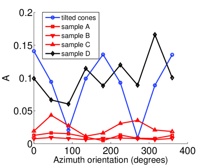
To examine if the samples give polarisation coupling, their Mueller matrices measured by MME have been analysed. If there is no coupling, the Mueller matrix should be block-diagonal. We define a measure of the degree of non-block-diagonality as
| (6) |
which is for block-diagonal Mueller matrices (such as reflections from isotropic surfaces), and has the value for maximum non-block-diagonal matrices (such as circular polarisers and linear polarisers). Figure 5 shows this quantity as a function of azimuth sample rotation around the mean surface normal for various samples. Additionally, as a reference, a sample with nanostructures sputtered at degrees of incidence, with an effective layer thickness of approximately is also shown [15, 16]. This sample consists of cones tilted by approximately degrees from the mean surface normal, and has as expected a Mueller matrix that is only block-diagonal for azimuthal orientations where the cones lie in the plane of incidence.
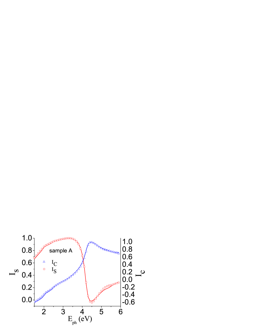
Moreover, it is observed from figure 5, that the short cone samples have negligible polarisation coupling, while the longer cones have substantial deviations from a block-diagonal Mueller matrix. This coupling could, as earlier discussed, be related to a slight tilting of the cones, to a long range preferential ordering of the cones, or an anisotropic shape of the individual cones. It is speculated that a long range preferential ordering could be induced by e.g. substrate polishing features. However, for sample , no azimuthal orientation has been observed to give a block-diagonal Mueller matrix, as should be the case for a thin film with the optic axis in the plane of incidence. This implies that these samples cannot be modelled as an anisotropic thin film layer, and that their optical properties are strongly affected by multiple scattering. Such samples can not be fully characterised by SE, and full Mueller matrix ellipsometry is instead necessary. The samples , and only show a slight deviation from block-diagonal Mueller matrices, and these off-diagonal elements will be neglected in the following analysis and modelling. The detailed analysis and modelling of tilted cones will be treated in a separate publication [16].
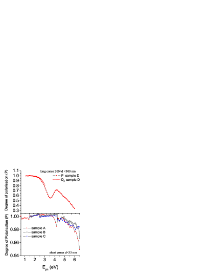
From the polarisation coupling at various azimuth orientations of sample , it was concluded that the polarisation altering properties of this sample had contributions from multiple scattering, and that it would not be well approximated as an effective media. From this conclusion, one would expect the sample to be depolarising, which is confirmed by the depolarisation index (, defined in equation (5)) evaluated from the MME measurements (figure 6). As expected, the depolarisation increase for increasing photon energy, since the effective medium approximation gets less accurate for decreasing wavelength. In addition, an approximation to the depolarisation at higher energies has been found by calculating the degree of polarisation, , from the PMSE measurements through equation (4). The degree of polarisation obtained in this way is a measure of how much certain polarisation states are depolarised, and will generally differ from the depolarisation index, which (in many cases) is the average depolarisation of all possible incident polarisation states (see [9]). For samples with block-diagonal Mueller matrices (, , ), the degree of polarisation can safely be used as a measure of depolarisation. It is observed that the short cones have principally a low depolarisation throughout the measured spectral range (figure 6). All the samples studied in the present work show an increasing depolarisation towards the UV range. Sample has a small dip in the degree of polarisation at the photon energy where and . This effect can be explained by a small variation in cone height (thin film thickness) [8] or cone shape. It could also be caused by quasi-monochromatic light from the monochromator. It is especially noted that the dielectric function is descending steeply at this photon energy [17], meaning that a very small wavelength distribution could give depolarisation. It is noted that samples and , show little depolarisation in the main part of the spectrum. This does not imply that these samples have less variation in cone height or shape than sample , since there is no photon energy for which and (see figure 3). All the short cones still show a small but observable increasing depolarisation for decreasing wavelength. Furthermore, it is observed that the degree of polarisation, , decreases more rapidly as a function of wavelength as the cone height increases.
3.3 Optical modelling
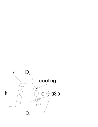
The cones with no or little depolarisation (”short-cones”) have been modelled as a graded anisotropic thin film layer of effective media, on a GaSb substrate. Reflection coefficients have been calculated by an implementation of Schubert’s algorithm [18] for reflections from arbitrarily anisotropic layered systems, based on Berreman’s differential matrices [19]. As a first approximation, the cones have been modelled as a stack of cylinders with decreasing diameter. Each cylinder in the stack defines a layer with a homogeneous effective dielectric function. With a sufficient number of layers, this will be a good approximation of a graded thin film layer. Based on HR-TEM observations, we have assumed the cylinders to consist of a core of crystalline GaSb, covered by a coating consisting of a mixture of amorphous GaSb and GaSb oxide. The anisotropy is introduced by using the generalised Bruggeman effective medium theory [20], giving the formula
| (7) | |||||
where and denote the filling factors and complex dielectric functions, respectively, with the subscript referring to the crystalline core, to the coating over layer, and to the surrounding void. denotes the depolarisation factor in direction (along a principal axis of the structure) and is the effective dielectric function in direction . Our principal axes will be two orthogonal axes parallel to the mean surface, and , and a axis normal to the mean surface. The dielectric function of the coating, , has been determined by letting it be a mixture of amorphous GaSb (a-GaSb) and GaSb oxide (oxide), and using the standard Bruggeman equation for spherical inclusions ()
| (8) |
These cylinders can thus be approximated as an effective thin film layer, which is valid when the distance between neighbouring cylinders are much smaller than the wavelength of the light. The layer will be anisotropic, with depolarisation factor in the plane parallel to the surface, and in the direction normal to the surface. The reflection coefficients from such an anisotropic layered system has been calculated, and used to find the ellipsometric intensities and [7]
| (9) |
| (10) |
The parameters of the models have been fitted to and by minimising , defined as
| (11) |
where N and M are the number of measurement points the number of free parameters in the model, respectively. and are the standard deviations of the respective measurements. Additional measurements such as any Mueller matrix element, or the reflectance, may be added to the formulae in a similar fashion.
The simplest model giving satisfying results has been one with 5 parameters (see figure 7), the total height , the relative (effective) diameters and of the bottom and top cylinder cores, the thickness of the coating , and the amount of oxide in the coating, . The two diameters and , and the thickness , are dimensionless quantities, defined as fractions of the mean nearest neighbour distance of the cones. This distance can not be found from the optical measurements when the effective medium approximation is valid, since the effective medium only depends on volume filling factors and shape through the depolarisation factors . This means that the model is independent of the scale in the horizontal plane, for all structures sufficiently smaller the the wavelength of light. A stack of =100 cylinders of equal height were used to approximate a continuous gradient, with the diameters of layer decreasing linearly from to :
| (12) |
for . Assuming a hexagonal ordering of the cylinders, the filling factor of crystalline GaSb and coating become:
| (13) |
and
| (14) |
Notice that for an effective medium theory it is only the filling factors that play a role, and not the specified ordering of the cones. As long as the filling factors remain the same, effective medium theory can not distinguish between different geometrical arrangements.The distance between the centers of neighbouring cones has been set to unit length. The thickness of coating is constant for all layers.
Minimisation was performed using the sequential quadratic programming (SQP) algorithm of the Matlab Optimisation Toolbox 3.1.1. The dielectric functions of crystalline GaSb, amorphous GaSb and GaSb oxide, were obtained from the literature [17, 21, 22]. The standard deviations (noise) and of the ellipsometric measurements and were estimated to be 0.01.
The resulting parameters of the fitted models are given in table 3. The model gave a good fit to the optical measurements of sample , with a cone height of , and a clear grading in the inner cylinder diameters from to . This is in good agreement with the previously presented SEM and TEM images (see figure 2).
Sample could be well fitted by a model with , meaning that it could have been modelled equally well by only one layer of coated cylinders. The cone height was found to be . It may be that the optical measurements are not sensitive to a possible gradient in such a short structure, or that the structures have a shape resembling a cylinder.
The ellipsometric measurements of sample greatly resemble those of sample , but the optical model could not give an equally good fit. When and are allowed to vary freely, the model converges to a seemingly unphysical case (based on the TEM and SEM images) with . To avoid this problem, they have been constrained so that . The result is then a cylinder like model (no grading), with a height of . It may appear to be necessary to develop more advanced models to perfectly fit the measurements of this sample. Natural extensions could be to let the coating thickness vary with height; letting the diameter d(n) of layer follow a non-linear function from to ; or letting the filling factors be able to deviate from values consistent with a hexagonal ordering. We will, however, not treat such advanced models here, but keep the parameters in the models to a minimum for easier interpretation, and to avoid unphysical solutions. It is also plausible that the dielectric functions of the different phases mixed in the effective medium theory are somehow different, e.g. that the properties of the oxide is different.
According to the results from the optical characterisation, sample should consist of slightly shorter cones than sample . This seems overall consistent with the AFM observations. It has been observed for sample , and that the nearest neighbour distance increase for increasing cone height (table 2). From the cone one should therefore expect sample to have shorter cones than sample . The average cone height estimated from AFM did not show as clear a difference between the samples, but such small height differences could possibly be masked in the uncertainty in the estimation of .
The height of the cones of sample and obtained from the optical model, are lower than the average heights found by AFM. It should be stressed that the height of sample (which coincided well with the height from the optical model) were found in a different way (by HR-TEM). As previously mentioned, the average cone height estimated from AFM measurements may be exaggerated. The model appears to be very sensitive to changes in the thickness of the effective medium layer, a perturbation in thickness of only a few nm results in a large increase of . However, different models may result in different layer thicknesses. For instance, it may seem more reasonable to let the cones be covered by a coating of thickness also on the top. This has been tested, and resulted in equally good values as the models reported in table 3, but with total heights – higher. The problem with such a model, is that the thickness of the coating top layer has to be determined absolutely, not just as a ratio, , of the nearest neighbour distance. This distance can not be obtained from SE measurements, but must be found from e.g. AFM or SEM studies. We are interested in a model that can help us characterise the nanostructures from SE measurements alone, and therefore reject this model with a coating also on the top.
The total volume filling factors for the optical models are tabulated in the last column of table 3. For ideal cones, ordered in a hexagonal lattice, the maximal filling factor is . The model filling factors lie in the range –, in good correspondence to the rounded conical structures observed from TEM, SEM and AFM measurements (rounded cones will give a larger filling factor than cones with a sharp top). Exact estimation of filling factors from microscopy images proved to be difficult. The varying shape and size of the individual cones must be taken into account, together with the mean nearest neighbour distance. The AFM measurements should in principle be ideal for this, but because of a too blunt tip and ”‘holes”’ in the surface, they drastically overestimate the filling factors. By estimating the shape and size of an individual cone from a TEM image, and using the mean nearest neighbour distance from AFM measurements, a rough estimation of the filling factor of sample A was found to be , in reasonable agreement with the value from the optical model ().
The construction of an effective medium optical model, predicts structural parameters that correspond reasonably well to the physical height of the samples, and the density/shape of the cones. Equally important, the models can by used to predict optical properties not measured. The model of sample , calibrated by SE measurements at angle of incidence, were used to successfully predict results of SE measurements at angle of incidence. The models may also predict the reflectance ( or ) of the samples (see figure 8). We propose that the models can be used as a tool to calculate the polarisation dependent optical properties of such samples at any angle of incidence.
The large depolarising properties of sample indicate that it may not be modelled appropriately by effective medium theory over the full spectral range considered. The experimental observations represent an interesting case, in the sense that there are no commonly available models to appropriately fit these data. A tentative effective medium modelling between and was tested in order to extract approximately the cone height of sample . It was found to be 165 nm, about half of the height found by SEM, but still considerably higher than heights found for the short cones, and with a clear gradient. The dielectric function data for GaSb-oxide and c-GaSb in the photon energy range –, were not available in the literature, and were therefore extrapolated from PMSE measurements at angle of incidence. The parameters of the resulting model are tabulated in order for completeness. Improved optical models suitable for modelling of the optical response of these samples are currently being undertaken, and planned for future work.
4 Summary and conclusions
Spectroscopic ellipsometry and Mueller matrix ellipsometry have been shown to be useful techniques for the characterisation of nanostructured surfaces, such as nanocones of GaSb on GaSb. Overall, the observations from SE appear to be consistent with the results from SEM, TEM and AFM studies. An optical model has been found to fit well to the measurements obtained for short cones (of height and lower).This was achieved by treating the structures as a graded anisotropic thin film of effective medium. These models have been applied in order to obtain an approximation to the average cone height of the samples, and also, to some extent to gain information on the cone shape. They may also be used to estimate reflectance and polarisation altering properties for reflections at any angle of incidence. The nanostructuration of the surface was shown to considerably reduce the reflectance. The antireflecting properties increased with cone height. Samples with long nanocones (–) were found to be strongly depolarising, and could not be modelled as an effective medium. The full Mueller matrix must be measured to fully characterise the polarisation altering properties of such samples. We have demonstrated that SE can be a fast and non-destructive way of characterising nanocones of GaSb, with the possibilities of in-situ control under production.
References
References
- [1] Born M and Wolf E 1980 Principles of optics. Electromagnetic theory of propagation, interference and diffraction of light (Oxford: Pergamon Press, 6th corrected ed.)
- [2] Beydaghyan G, Buzea C, Cui Y, Elliott C and Robbie K 2005 Appl. Phys. Lett. 87 153103
- [3] Yang Z P, Ci L, Bur J A, Lin S Y and Ajayan P M 2008 Nano Lett. 8 446–451
- [4] Facsko S, Dekorsy T, Koerdt C, Trappe C, Kurz H, Vogt A and Hartnagel H L 1999 Science 285 1551–1553
- [5] Brun N, Søndergård E, Lelarge A and Barthel E (Unpublished)
- [6] Drévillon B 1993 Prog. Cryst. Growth Charact. 27 1–87
- [7] Hauge P 1980 Surface Science 96 81–107
- [8] Jellison Jr G E and McCamy J W 1992 Appl. Phys. Lett 61 512–514
- [9] Chipman R A 2005 Appl. Opt. 44 2490–2495
- [10] Weaire D and Rivier N 1984 Contemp. Phys. 25 55–99
- [11] Bernhard C G 1967 Endeavour 26 79–84
- [12] Azzam R M A and Bashara N M 1987 Ellipsometry and Polarized Light (NORTH-HOLLAND)
- [13] Jellison G E and Modine F A 1997 Appl. Opt. 36 8190–8198
- [14] Laskarakis A, Logothetidis S, Pavlopoulou E and Gioti M 2004 Thin Solid Films 455-456 43–49
- [15] Kildemo M, Nerbø I S, Søndergård E, Holt L, Simonsen I and Stachakovsky M 2008 phys. stat. sol. (c) 5 1382 1385
- [16] Nerbø I S, Kildemo M, Hagen S W, Leroy S and Søndergård E Optical properties and characterisation of tilted gasb nanocones (To be published)
- [17] Aspnes D E and Studna A A 1983 Phys. Rev. B 27 985–1009
- [18] Schubert M 1996 Phys. Rev. B 53 4265–4274
- [19] Berreman D W 1972 J. Opt. Soc. Am. 62 502–510
- [20] Spanier J E and Herman I P 2000 Phys. Rev. B 61 10437–10450
- [21] Stuke J and Zimmerer G 1972 phys. stat. sol. (b) 49 513–523
- [22] Zollner S 1993 Appl. Phys. Lett 63 2523–2524
-
Sample name Sputter Time Mean Temperature Applied Voltage Average Flux (min) (∘C) (V)
-
Sample name Density (nm) (nm) () (nm) degrees
-
Sample name (nm)