Enhanced Zeeman splitting in Ga0.25In0.75As quantum point contacts
Abstract
The strength of the Zeeman splitting induced by an applied magnetic field is an important factor for the realization of spin-resolved transport in mesoscopic devices. We measure the Zeeman splitting for a quantum point contact etched into a Ga0.25In0.75As quantum well, with the field oriented parallel to the transport direction. We observe an enhancement of the Landé g-factor from for the third subband to for the first subband, six times larger than in GaAs. We report subband spacings in excess of 10 meV, which facilitates quantum transport at higher temperatures.
pacs:
73.21.Hb, 71.70.Ej, 85.75.-dThe control of a charge carrier’s spin is typically achieved using an applied magnetic field, and provides an extra degree of freedom that can be utilized for device functionalities such as spintronics, quantum information, etc. Wolf et al. (2001); Elzerman et al. (2004); Craig et al. (2004); Tombros et al. (2006) In semiconductor devices, the field breaks the degeneracy of the two spin states via the Zeeman effect, resulting in spin-polarized transport, where a particular spin orientation dominates the electrical conductance of the device. Wolf et al. (2001); Elzerman et al. (2004) The Zeeman spin-splitting is given by , where is the effective Landé g-factor and is the Bohr magneton. Since the strength of the spin-splitting is governed by , narrow band-gap materials with a large -factor such as GaInAs or InAs are highly desirable in the quest to develop electronic devices that require only the smallest magnetic fields to achieve spin-functional operations.
The small band-gap in the GaxIn1-xAs material system makes a large -factor possible due to mixing of the conduction band electron states with valence band states. For example, in GaInAs quantum wells, -factors ranging from 2.9 to 4.4 have been measured Vehse et al. (1986); Dobers et al. (1989); Savel’ev et al. (1996); Schäpers et al. (2007) – an order of magnitude larger than in equivalent GaAs quantum wells. Dobers et al. (1988, 1989) It is thus interesting to know how the -factor in lower-dimensional structures will behave, because the additional confinement alters the coupling between the conduction and valence bands. In both -type and -type GaAs quantum point contacts (QPCs), the confinement of electrons to a quasi-one-dimensional (quasi-1D) system can lead to an enhancement of by as much as a factor of two over its 2D value, with the enhancement increasing as the 1D confinement is strengthened. Patel et al. (1991a); Thomas et al. (1996); Daneshvar et al. (1997); Danneau et al. (2006) Unexpectedly, the only measurement to date of the -factor in a GaInAs QPC Schäpers et al. (2007) gave in the 1D limit, showing no clear enhancement over the value of obtained in the 2D reservoirs adjacent to the QPC. Schäpers et al. (2007)
In this letter, we use parallel field measurements (oriented in the plane of the quantum well along the QPC) to study how the strength of the 1D confinement affects the spin-splitting in an etched Ga0.25In0.75As QPC. In contrast to the measurements obtained using perpendicular fields by Schäpers et al., Schäpers et al. (2007) we observe a clear enhancement of the -factor in the 1D limit of our device. Our result is consistent with the 1D enhancement observed in GaAs QPCs, which was also measured using parallel field techniques. Patel et al. (1991a); Thomas et al. (1996); Daneshvar et al. (1997); Danneau et al. (2006) The key difference between our measurements and those of Reference 8 is the field direction, and we use this to explain why 1D -factor enhancement was not observed in their study.
Our QPC is etched into a GaInAs/InP modulation-doped heterostructure, where a 2D electron gas (2DEG) is confined to a 9 nm thick Ga0.25In0.75As quantum well. Ramvall et al. (1997); Martin et al. (2008) The QPC investigated is 160 nm long and 120 nm wide, and fabricated on a Hall bar mesa featuring NiGeAu Ohmic contacts. A Ti/Au top-gate, deposited uniformly over the mesa, is used to tune the Fermi energy and thus change the number of occupied subbands in the QPC. All measurements were performed in a 4He cryostat with a base temperature of 1.3 K. Standard four-probe and lock-in amplification techniques were used to measure the differential conductance through the QPC at a frequency of 17 Hz and constant excitation voltage of 100 V (300 V for source-drain biasing). The 2D carrier density and mobility were 5.6–6.8 cm-2 and 1.3–2.2 cm2/Vs respectively within the range of applied gate voltages presented here ( to 1.5 V). Our 2D density and mobility, gallium fraction , and quantum well width are very similar to the values reported in Ref. 8.
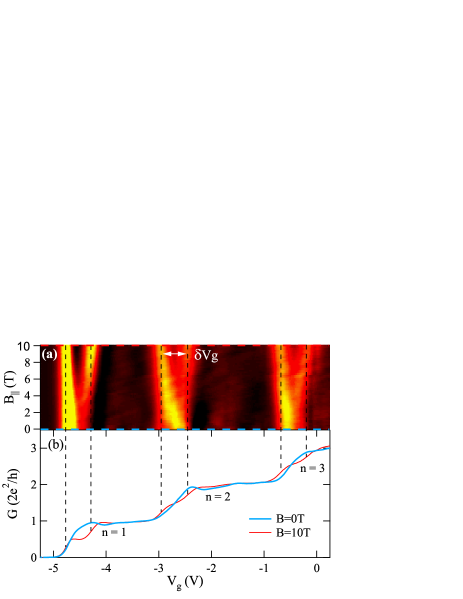
The blue line in Figure 1(b) shows the conductance of the QPC at , demonstrating clear plateaux as a function of gate voltage . The plateaux are a consequence of the 1D confinement in the QPC, where each occupied subband contributes to the conductance. An in-plane magnetic field was applied parallel to the direction of transport in the QPC to induce Zeeman splitting. At T, the spin-degeneracy is lifted (red line in Fig. 1(b)) and the conductance is quantized in units . The evolution of the spin splitting with applied magnetic field is shown in Fig. 1(a), where the transconductance is plotted as a function of the gate voltage and magnetic field. The light regions mark the 1D subband edges, corresponding to the rises between conductance plateaux where is maximum. The spin-splitting increases with applied magnetic field, which is observed as an increasingly large splitting between the bright regions in Fig. 1(a).
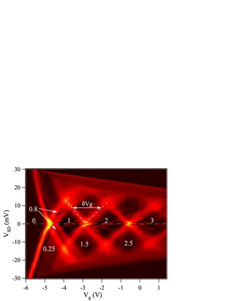
Unfortunately, the splitting cannot be obtained directly from Fig. 1(a), which only gives . To calculate the -factor, it is necessary to convert into the subband energy scale, which is achieved by measuring the splitting in gate voltage due to an applied d.c. source-drain bias . We do this using the method developed by Patel et al. Patel et al. (1991a) that combines measurements of the splitting due to the field (Fig. 1(a)) with measurements of the splitting due the source-drain bias to give the absolute value of the -factor:
| (1) |
The source-drain bias measurements are shown in Fig. 2, where the transconductance is plotted as a function of and at (data have been corrected for the d.c. bias dropped across the series resistance). Similar to Fig. 1(a), the light regions correspond to the transitions between 1D subbands (large ), marking the 1D subband edges. As the applied bias is increased, the subband transitions (light regions) split in gate voltage by , and conductance plateaux at half-integer appear between the split transitions. Patel et al. (1991b); Kristensen et al. (2000) Since the splitting is directly proportional to , the energy scales associated with in Fig. 2 are obtained by calculating . Patel et al. (1991b); Kristensen et al. (2000)
The transconductance maxima in Fig. 2 cross when the applied source-drain bias is equal to the subband spacing: , Patel et al. (1991b); Kristensen et al. (2000) allowing the subband spacing to be directly extracted from Fig. 2. Values of calculated from these crossing points are listed in Table 1 and exceed 10 meV. The subband spacings are consistent with those obtained using magnetic depopulation measurements, Martin et al. (2008) and are double the spacings measured for etched In0.47Ga0.53As quantum wires with InAlAs barriers. Sugaya et al. (2001) In Refs. 16 and 17 the ‘0.7 feature’ evolves into plateaux with at finite source-drain bias. In Fig. 2, we observe similar ‘shoulder’ plateaux with , despite there being no clear 0.7 feature at . Oscillatory structure is also observed on the conductance plateaux in Fig. 2, which has recently been linked to standing waves in the QPC Lindelof and Aagesen (2008) and will be discussed elsewhere.
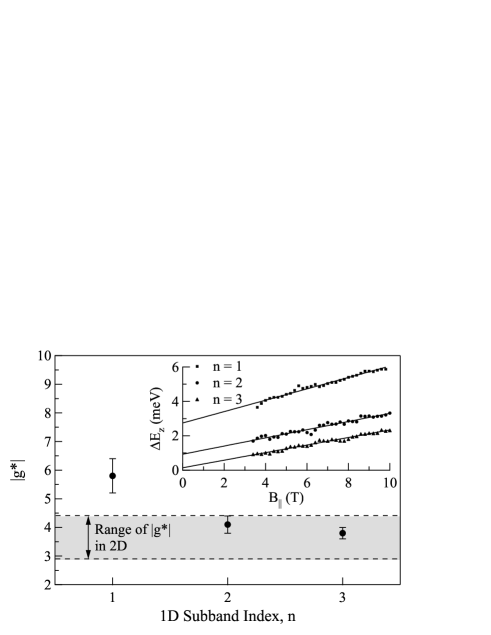
The Zeeman energies and -factors are calculated using Equation (1) and the data extracted from Figs. 1 and 2. The splitting rates and are listed in Table 1. The Zeeman splitting of the 1D subbands is plotted against in the inset of Fig. 3, demonstrating a linear relationship for T where the subband transitions are clearly resolved. Although the linear fits for the first two subbands do not extrapolate to zero at (due to the presence of the 0.7 feature and its analog at 1.7), still the -factor can be extracted for each subband using Eq. (1). Patel et al. (1991a); Thomas et al. (1996) The values of are plotted as a function of in Fig. 3. For the and subbands, we find that falls within the range previously reported for 2D GaxIn1-xAs systems. Vehse et al. (1986); Dobers et al. (1989); Savel’ev et al. (1996); Schäpers et al. (2007) However, in contrast with Ref. 8, we obtain for , confirming the presence of a 1D enhancement in our Ga0.25In0.75As QPC.
In Ref. 8, the Zeeman splitting was measured with fields 3 T T applied perpendicular, rather than parallel, to the quantum well. This produces magnetic confinement due to Landau quantization that adds to the QPC’s electrostatic confinement. Ref. 8 reports 1D subband spacings that are smaller than the Landau level spacing for these fields. Schäpers et al. (2007) This is a non-physical result, since the addition of 1D confinement to a 2D system in a perpendicular field cannot decrease the energy level spacing. For example, the 1D subband spacing is reported to be only 8.4 meV at T when the 2D Landau level spacing is already 11.9 meV. Schäpers et al. (2007) Thus we suggest that the value of reported in Ref. 8 has been underestimated, which explains why no enhancement was observed. In contrast, our data are obtained with an in-plane magnetic field in the absence of Landau quantization. Our measurements show an enhancement of the -factor as the QPC becomes more one-dimensional in agreement with previous results in 1D GaAs systems. Patel et al. (1991a); Thomas et al. (1996); Daneshvar et al. (1997); Danneau et al. (2006)
In summary, we have demonstrated that 1D confinement in a narrow-gap semiconductor such as GaInAs can result in a significant enhancement of the Zeeman splitting. Although the enhancement in is consistent with the trend observed in GaAs QPCs, Patel et al. (1991a); Thomas et al. (1996); Daneshvar et al. (1997); Danneau et al. (2006) the magnitude of measured for GaInAs QPCs is six times greater. Additionally, the subband spacing in our devices is quite large. Martin et al. (2008) Combined, the large -factors and subband spacings found in etched GaInAs QPCs make them suitable for applications requiring spin-sensitivity at higher temperatures and with small magnetic fields.
We acknowledge financial support by the Australian Research Council, the National Science Foundation, and the Research Corporation.
References
- Wolf et al. (2001) S. A. Wolf, D. D. Awschalom, R. A. Buhrman, J. M. Daughton, S. von Molnar, M. L. Roukes, A. Y. Chtchelkanova, and D. M. Treger, Science 294, 1488 (2001).
- Elzerman et al. (2004) J. M. Elzerman, R. Hanson, L. H. W. van Beveren, B. Witkamp, L. M. K. Vandersypen, and L. P. Kouwenhoven, Nature 430, 431 (2004).
- Craig et al. (2004) N. J. Craig, J. M. Taylor, E. A. Lester, C. M. Marcus, M. P. Hanson, and A. C. Gossard, Science 304, 565 (2004).
- Tombros et al. (2006) N. Tombros, S. J. van der Molen, and B. J. van Wees, Phys. Rev. B 73, 233403 (2006).
- Vehse et al. (1986) D. L. Vehse, S. G. Hummel, H. M. Cox, F. DeRosa, and S. J. Allen, Phys. Rev. B 33, 5862 (1986).
- Dobers et al. (1989) M. Dobers, J. P. Vieren, Y. Guldner, P. Bove, F. Omnes, and M. Razeghi, Phys. Rev. B 40, 8075 (1989).
- Savel’ev et al. (1996) I. G. Savel’ev, A. M. Kreshchuk, S. V. Novikov, A. Y. Shik, G. Remenyi, G. Kovács, B. Pôdör, and G. Gombos, J. Phys.: Condens. Matter 8, 9025 (1996).
- Schäpers et al. (2007) T. Schäpers, V. A. Guzenko, and H. Hardtdegen, Appl. Phys. Lett. 90, 122107 (2007).
- Dobers et al. (1988) M. Dobers, K. von Klitzing, and G. Weimann, Phys. Rev. B 38, 5453 (1988).
- Patel et al. (1991a) N. K. Patel, J. T. Nicholls, L. Martín-Moreno, M. Pepper, J. E. F. Frost, D. A. Ritchie, and G. A. C. Jones, Phys. Rev. B 44, 10973 (1991a).
- Thomas et al. (1996) K. J. Thomas, J. T. Nicholls, M. Y. Simmons, M. Pepper, D. R. Mace, and D. A. Ritchie, Phys. Rev. Lett. 77, 135 (1996).
- Daneshvar et al. (1997) A. J. Daneshvar, C. J. B. Ford, A. R. Hamilton, M. Y. Simmons, M. Pepper, and D. A. Ritchie, Phys. Rev. B 55, R13409 (1997).
- Danneau et al. (2006) R. Danneau, O. Klochan, W. R. Clarke, L. H. Ho, A. P. Micolich, M. Y. Simmons, A. R. Hamilton, M. Pepper, D. A. Ritchie, and U. Zülicke, Phys. Rev. Lett. 97, 026403 (2006).
- Ramvall et al. (1997) P. Ramvall, N. Carlsson, I. Maximov, P. Omling, L. Samuelson, W. Seifert, Q. Wang, and S. Lourdudoss, Appl. Phys. Lett. 71, 918 (1997).
- Martin et al. (2008) T. P. Martin, C. A. Marlow, L. Samuelson, A. R. Hamilton, H. Linke, and R. P. Taylor, Phys. Rev. B 77, 103811 (2008).
- Patel et al. (1991b) N. K. Patel, J. T. Nicholls, L. Martín-Moreno, M. Pepper, J. E. F. Frost, D. A. Ritchie, and G. A. C. Jones, Phys. Rev. B 44, 13549 (1991b).
- Kristensen et al. (2000) A. Kristensen, H. Bruus, A. E. Hansen, J. B. Jensen, P. E. Lindelof, C. J. Marckmann, J. Nygård, C. B. Sørensen, F. Beuscher, A. Forchel, et al., Phys. Rev. B 62, 10950 (2000).
- Sugaya et al. (2001) T. Sugaya, M. Ogura, Y. Sugiyama, T. Shimizu, K. Yonei, K. Y. Jang, J. P. Bird, and D. K. Ferry, Appl. Phys. Lett. 79, 371 (2001).
- Lindelof and Aagesen (2008) P. E. Lindelof and M. Aagesen, J. Phys.: Condens. Matter 20, 164207 (2008).
| Parameter | ||||
|---|---|---|---|---|
| (meV) | ||||
| (V/T) | ||||
| (meV/V) | ||||
| - - |