Band Offsets at the Si/SiO2 Interface from Many-Body Perturbation Theory
Abstract
We use many-body perturbation theory, the state-of-the-art method for band gap calculations, to compute the band offsets at the Si/SiO2 interface. We examine the adequacy of the usual approximations in this context. We show that (i) the separate treatment of band-structure and potential lineup contributions, the latter being evaluated within density-functional theory, is justified, (ii) most plasmon-pole models lead to inaccuracies in the absolute quasiparticle corrections, (iii) vertex corrections can be neglected, (iv) eigenenergy self-consistency is adequate. Our theoretical offsets agree with the experimental ones within 0.3 eV.
pacs:
71.10.-w,73.40.Ty,73.40.Lq,85.40.-e,85.60.-qThe band offsets (BOs) are among the most important properties of a heterostructure. Their precise knowledge is extremely important to engineer electronic Wilk2001 and optoelectronic Morteani2004 devices. Various theoretical methods have been used to estimate the BOs Tejedor1978-Harrison1980-Tersoff1984-Robertson2000-Peacock2002 ; VandeWalle1986 ; Yamasaki2001 . Among these, density functional theory (DFT) calculations allow one to study the variation of interface dipoles with the interface structure, without resorting to experimental input VandeWalle1986 .
In the DFT approach, the valence band offset (VBO) and the conduction band offset (CBO) are conveniently split into two terms: . The first term , referred to as the band-structure contribution, is defined as the difference between the valence band maxima (VBM) or the conduction band minima (CBM) relative to the average of the electrostatic potential in each material. These are obtained from two independent standard bulk calculations on the two materials. The second term , called the lineup of the average of the electrostatic potential across the interface, accounts for all the intrinsic interface effects. It is determined from a supercell calculation with a model interface.
However, the DFT-BOs suffer from two important limitations, namely, the well-known DFT band-gap problem, and the use of an approximate functional to model the exchange-correlation (XC) energy, such as the local density approximation (LDA) or the generalized gradient approximation (GGA). These affect the value of the VBM and the CBM, and consequently the calculated BOs. Orbital-dependent approaches Kummel2008 and many-body perturbation-theory (MBPT) within the approximation Hedin1965 have been used to try to overcome these shortcomings Devynck2007 ; Zhang1988 ; Zhu1991 . While the former may be less computationally demanding, their reliability cannot be assessed a priori Kummel2008 in contrast with MBPT. In Refs. Zhang1988 ; Zhu1991 , the lineup of the potential was approximated by its DFT value, arguing that it depends primarily on the charge distribution at the interface which is a ground state quantity, hence little affected by many-body effects. Doing so, only the band-structure contribution is modified:
| (1) |
where () is the quasiparticle (QP) correction at the VBM (CBM): for . It is important to stress that these corrections, which are obtained from bulk calculations, are the only additional ingredients that are required when DFT calculations of the VBO and CBO already exist.
Interestingly, for various semiconductor interfaces, the QP corrections of the band edges are found to be almost the same on both sides Zhu1991 leading to 0.2 eV in Eq. (1). As a result of this cancellation of errors, DFT is quite successful for the same interfaces VandeWalle1987 with errors ranging from 0.1 to 0.5 eV, despite its limitations mentioned above. This relative success of DFT explains why it has been widely used to predict the VBO for a wide range of interfaces. And, when needed, the CBO was also predicted using a simple scissor operator to correct the band gap to the experimental value. This assumption was further motivated by the fact that MBPT calculations going beyond by including an approximate vertex correction () showed that the valence-band-edge energy remained at its DFT value for silicon, the whole correction going to the conduction bands DelSole1994 ; Fleszar1997 .
However, when it comes to semiconductor-insulator or insulator-insulator interfaces, it appears that the DFT errors on the VBO can be much more important. For instance, for the Si/SiO2 interface, the VBO are calculated to be 2.3-3.3 eV Yamasaki2001 ; Watarai2004 ; Tuttle2004 ; Giustino2005a in noticeable disagreement with the experimental results of 4.3 eV Experiments . It seems that, for such systems, the cancellation of errors is not as good, emphasizing the need to go beyond DFT by including QP corrections. The same is probably true for interfaces found in transistors or organic photovoltaics. Before applying such a highly-demanding method in a predictive way, its quality needs to be assessed for an interface for which the VBO and CBO are well-known experimentally, such as the Si/SiO2 one.
In this Letter, the effect of QP corrections on the VBO and CBO at the Si/SiO2 interface is investigated. By performing a quasiparticle self-consistent (QS) calculation on a small interface model, we demonstrate that the line up potential is well described in DFT. For two more realistic models, the BOs calculated within DFT are corrected by computing the QP corrections for bulk Si and SiO2. The latter are found to be crucial to reach a good agreement with experimental results. Their effect can not be accounted for by a simple scissor operator on top of DFT results. The inclusion of the vertex correction is shown not to affect the results significantly, whereas QS does not improve the results.
Three different interface models are adopted in which ideal -cristobalite is matched to the Si(100) surface, taking the theoretical value of bulk Si (=5.48 Å) as the lattice constant. The models I and II were generated in a previous work by two of us Giustino2005a in order to calculate the BOs within DFT. They consist of 11 Si monolayers and up to 10 SiO2 molecular layers which guarantees well converged BOs. Model III is limited to 8 Si monolayers and 8 SiO2 molecular layers in order to perform a QS calculation which is quite demanding computationally. For bulk Si, the theoretical value is adopted for the lattice constant. For SiO2, we consider on the one hand the cubic structure (space group ) whose relaxed lattice constant is =7.43 Å; and, on the other hand, a tetragonal structure (space group ) in which two sides are strained to match the Si lattice constant = as in the interface models of Ref. Giustino2005a , while the third is left free to relax reaching a value of =6.59 Å. In both structures, the Si-O-Si bond angle is 180∘. Hereafter, the cubic and strained structures will be referred to as c-SiO2 and s-SiO2, respectively.
All our calculations are performed using the ABINIT package Gonze2005 . Only valence electrons are explicitly considered using norm-conserving pseudopotentials Troullier1991 to account for core-valence interactions. By coherence with the DFT calculations of the BOs Giustino2005a , the XC energy is also described within the GGA Perdew1992 .
At the DFT level, the band gaps for the bulk systems are found to be 0.7 eV for Si, 5.4 eV for c-SiO2, and 5.1 eV for s-SiO2 note:bulk . For the interface models I and II, the VBOs (CBOs) are calculated to be 2.6 and 2.5 eV (1.6 and 1.8 eV), respectively note:interface .
Three approaches are used to compute the QP corrections. In the first approach (), the self-energy is calculated self-consistently by updating the eigenenergies in both the dielectric matrices and the Green’s functions while keeping the DFT wavefunctions. In the second approach (QS), both the eigenenergies and the wavefunctions are updated Faleev2004 . In both approaches, the dielectric matrices are computed in the random-phase approximation (RPA) using the sum over states formulation Adler1962-Wiser1963 . In the third approach, a vertex correction is included in both the screening and the self-energy by going beyond the RPA and including XC effects DelSole1994 , and only the eigenergies are updated. Details about the DFT-GGA kernel are provided in Ref. DalCorso1994 .
Within , the frequency dependence of the dynamically screened Coulomb potential is most often approximated using various plasmon pole models (PPMs) Hybertsen1986 ; vonderLinden1988 ; Godby1989 ; Engel1993 . The advantage is not only to reduce the computational load, but also to obtain an analytic expression for the self-energy. In fact, PPMs have proven to be very effective in producing band gaps in good agreement with experiments.
However, while the QP correction to the gap was found not to be very sensitive to the choice of the PPM Arnaud2000 , we observe that and may vary from one PPM to another, as reported in Table 1 for Si and c-SiO2. In particular, the variation of with the PPM is more pronounced in c-SiO2 (up to 0.4 eV difference between the extreme cases) than in Si. Since a precise knowledge of the QP corrections at the band edges is required for the band offsets calculations, it is necessary to go beyond PPMs taking explicitly into account the frequency dependence of .
| HL | vdLH | GN | EF | no PPM | ||
|---|---|---|---|---|---|---|
| Si | ||||||
| c-SiO2 | ||||||
In this work, the explicit frequency dependence is obtained using the deformed contour integration technique Lebegue2003 . The calculated QP corrections are reported in Table 2 for Si, c-SiO2, and s-SiO2.
The QP gaps can easily be obtained from these results . Within , =1.3 eV for Si and 8.8 eV for c-SiO2. These results are in good agreement with the experimental values of 1.2 and 8.9 eV DiStefano1971 , respectively. While results (1.3 and 8.5 eV) are very close, the QS results (1.5 and 9.5 eV) are overestimated like systematically observed in Ref. Shishkin2007 .
| Si | c-SiO2 | s-SiO2 | |||||||||
|---|---|---|---|---|---|---|---|---|---|---|---|
| GW | GWΓ | GW | GWΓ | GW | GWΓ | ||||||
Turning to and , the comparison of our results with previous calculations is not always straightforward. In most of the cases, the focus is on the band gap and the QP corrections are not given explicitly (the VBM is set to zero after correction). Besides, and are very sensitive to the degree of convergence reached (the QP gap converges much faster than the QP corrections), not to mention the effect of the PPM (see Table 1). For Si, our and results compare quite well with those of Fleszar and Hanke Fleszar1997 which also do not rely on any PPM note:Fleszar . No such comparison can be made for c-SiO2. Note however that the QP corrections for c-SiO2 and s-SiO2 differ by up to 0.2 eV, indicating a dependence of and on the strain. This is at variance with the findings of Ref. Zhu1989 in the case of Si under isotropic strain. A possible explanation for this difference may be that the strain is not isotropic in s-SiO2 note:bulk . Finally, note that the PPM proposed by Godby and Needs Godby1989 leads to QP corrections (see Table 1) in excellent agreement with those of the contour deformation method, at variance with the other PPMs. This finding might be generalized after proper investigation.
While and QS lead to a lowering of the VBM of Si (slightly larger for QS) compared to the DFT result, the inclusion of the vertex correction brings it back to roughly its original value with a small shift of 0.1 eV, all the QP correction being on the conduction band. A similar result was also found previously DelSole1994 ; Fleszar1997 giving some motivation to the use of a scissor operator to compute the CBO within DFT. For SiO2, our results are very different. First, the VBM is also raised when going from to , but it definitely does not reach the DFT level back. This indicates the recovery of the DFT VBM with is a coincidence in Si. And, it definitely rules out the use of a simple scissor operator for the computation of the BOs. Second, the lowering of the VBM in QS in much larger than in (by about 0.9 eV). In fact, it seems that the systematical overestimation of the band gap in QS originates essentially from a too strong lowering of the VBM. Note that the increase of the CBM is slightly lower in QS than in .
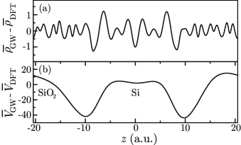
In order to compute the QP corrections to the BOs, the many-body effects on also need to be investigated. This is done by comparing the electronic density and the resulting calculated within DFT and QS for model III. In Fig. 1(a), the difference between the planar average of the DFT electronic density and the QS one is reported. The QS result differs only slightly from DFT, with a maximum change of about 1 m/a.u. in the interface region. The difference between the QS and DFT macroscopic average of the local potential , which is reported in Fig. 1(b), is about 45 meV in the interface region, and less than 12 meV in the bulk regions. This gives rise to a net difference of 20 meV in the lineup of the potential . Such a small difference in suggests that the interfacial charge density and, consequently, the associated dipole moments are well described within DFT. This justifies the assumption that the line up potential can be taken to be the same as in DFT.
Finally, using Eq. (1), the band offsets can be computed within MBPT at the , , and QS levels. Our results are reported in Table 3 and compared with the experimental ones. Within the agreement is excellent for both the VBO and CBO (less than 0.3 eV difference). The effect of the vertex correction is less than 0.1 eV on the BOs. This results from a cancellation of the effects on each side of the interface. At this stage, we cannot say whether this result can be generalized to any interface. In contrast, the effect of quasiparticle self-consistency is more pronounced. Due to the large lowering of the VBM of SiO2, the VBO is increased by 0.7 eV compared to , leading to an overestimation by up to 0.5 eV. At the same time, the CBO is slightly smaller than in leading to an underestimation by up to 0.6 eV. So that QS is the worst of the three approaches.
| cubic | strained | |||||||||||
|---|---|---|---|---|---|---|---|---|---|---|---|---|
| GW | GWΓ | GW | GWΓ | |||||||||
| VBO | I | 2.6 | 4.1 | 4.0 | 4.8 | 4.1 | 4.0 | 4.8 | 4.3 | |||
| II | 2.5 | 4.0 | 3.9 | 4.7 | 4.0 | 3.9 | 4.7 | |||||
| CBO | I | 1.6 | 2.9 | 2.7 | 2.7 | 2.8 | 2.7 | 2.5 | 3.1 | |||
| II | 1.8 | 3.1 | 2.9 | 2.9 | 3.0 | 2.9 | 2.7 | |||||
In summary, we have investigated the band offsets at the Si/SiO2 interface using many-body perturbation theory. Starting from the BOs obtained within DFT for two model interfaces, the QP corrections have been computed within eigenenergy self-consistent and , and quasiparticle self-consistent taking the frequency dependence of the screened potential explicitly into account (which is more reliable than plasmon pole models). The corrections, which differ significantly from what can be obtained using a scissor operator, produce BOs in excellent agreement with experiment. While the BOs obtained with and without vertex correction do not differ significantly, those resulting from QS present a larger deviation from experiments. These findings allow us to recommend the use of eigenenergy self-consistent , which is less demanding. Now that the quality of the procedure has been assessed, it can be used in a predictive way for heterojunctions of high technological interest such as those in transistors or organic photovoltaics.
Acknowledgements.
This work was supported by the EU FP6 and FP7 through the Nanoquanta NoE (NMP4-CT-2004-50019) and the ETSF I3 e-Infrastructure (Grant Agreement 211956), and the project FRFC N∘. 2.4502.05.References
- (1) G.D. Wilk, R.M. Wallace, and J.M. Anthony, J. Appl. Phys. 89, 5243 (2001).
- (2) A.C. Morteani, et al., Phys. Rev. Lett. 92, 247402 (2004).
- (3) C. Tejedor and F. Flores, J. Phys. C 11, L19 (1978); W.A. Harrison, Electronic Structure and the Properties of Solids (Freeman, San Francisco, 1980), p. 253; J. Tersoff, Phys. Rev. B 30, 4874 (1984); J. Robertson, J. Vac. Sci. Technol. B 18, 1785 (2000); P.W. Peacock and J. Robertson, Appl. Phys. 92, 4712 (2002).
- (4) C.G. Van de Walle and R.M. Martin, Phys. Rev. B 34, 5621 (1986).
- (5) T. Yamasaki et al., Phys. Rev. B 63, 115314 (2001).
- (6) S. Kümmel and L. Kronik. Rev. Mod. Phys. 80, 3 (2008).
- (7) L. Hedin, Phys. Rev. 139, A796 (1965).
- (8) F. Devynck, F. Giustino, P. Broqvist, and A. Pasquarello. Phys. Rev. 76, 075351 (2007).
- (9) S. B. Zhang et al., Solid State Commun. 66, 585 (1988).
- (10) X. Zhu and S. G. Louie, Phys. Rev. B 43, 14142 (1991).
- (11) C.G. Van de Walle and R.M. Martin, Phys. Rev. B 35, 8154 (1987).
- (12) R. Del Sole, L. Reining, and R.W. Godby, Phys. Rev. B 49, 8024 (1994).
- (13) A. Fleszar and W. Hanke, Phys. Rev. B 56, 10228 (1997).
- (14) M. Watarai, J. Nakamura, and A. Natori, Phys. Rev. B 69, 035312 (2004).
- (15) B.R. Tuttle, Phys. Rev. B 70, 125322 (2004).
- (16) F. Giustino and A. Pasquarello, Surf. Sci. 586 183 (2005).
- (17) J.W. Keister et al., J. Vac. Sci. Technol. B 17, 1831 (1999); V.V. Afanas’ev, M. Houssa, and A. Stesman, Appl. Phys. Lett. 78, 3073 (2001).
- (18) X. Gonze et al., Zeit. Kristall. 220, 558 (2005).
- (19) N. Troullier and J.L. Martins, Phys. Rev. B 43, 1993 (1991).
- (20) J.P. Perdew, et al., Phys. Rev. B 46, 6671 (1992).
- (21) For Si, the gap is indirect with the VBM located at and the CBM approximated by the point; while c-SiO2 has a direct gap at . The lowering of the symmetry in s-SiO2 results in a splitting of the threefold-degenerate state at into two top valence states, the highest corresponding to the orbital, and the other (twofold-degenerate) to the and orbitals. These two states are separated by 0.27 eV, accounting basically for the difference in the band gap between the two SiO2 structures.
- (22) In Ref. Giustino2005a , the BOs were obtained directly from the local density of states in the supercell. The difference between the two models was attributed to different interface dipoles. Interestingly, the calculated BOs are almost identical to those of more sophisticated models in which the SiO2 side is taken to be disordered Giustino2005b , justifying further comparison with experiments in which the silica is amorphous. Note that the band gaps calculated directly in the interface models are slightly smaller than those of the bulk calculations probably due to the lowering of the symmetry resulting from the atomic relaxation.
- (23) S.V. Faleev, M. van Schilfgaarde, T. Kotani, Phys. Rev. Lett. 93, 126406 (2004).
- (24) L. Adler, Phys. Rev. 126, 413 (1962); N. Wiser, ibid. 129, 62 (1963).
- (25) A. Dal Corso, S. Baroni, and R. Resta Phys. Rev. B 49, 5323 (1994).
- (26) M.S. Hybertsen and S.G. Louie, Phys. Rev. B 34, 5390 (1986).
- (27) W. von der Linden and P. Horsch, Phys. Rev. B 37, 8351 (1988).
- (28) R.W. Godby and R.J. Needs, Phys. Rev. Lett. 62, 1169 (1989).
- (29) G.E. Engel and B. Farid, Phys. Rev. B 47, 15931 (1993).
- (30) B. Arnaud and M. Alouani, Phys. Rev. B 62, 4464 (2000).
- (31) S. Lebègue, B. Arnaud, M. Alouani and P. E. Bloechl, Phys. Rev. B 67, 155208 (2003).
- (32) T.H. Di Stefano and D.E. Eastman, Solid Stat. Comm. 9, 2259 (1971).
- (33) M. Shishkin, M. Marsman, and G. Kresse, Phys. Rev. Lett. 99, 246403 (2007).
- (34) The slight differences are probably due to the use of a different XC energy functional at the DFT level (GGA in our case and LDA in the work of Fleszar and Hanke).
- (35) X. Zhu, S. Fahy, and S.G. Louie, Phys. Rev. B 39, 7840 (1989).
- (36) F. Giustino, A. Bongiorno, and A. Pasquarello Appl. Phys. Lett. 86, 192901 (2005).