Running a Quantum Circuit at the Speed of Data
Abstract
We analyze circuits for a number of kernels from popular quantum computing applications, characterizing the hardware resources necessary to take ancilla preparation off the critical path. The result is a chip entirely dominated by ancilla generation circuits. To address this issue, we introduce optimized ancilla factories and analyze their structure and physical layout for ion trap technology. We introduce a new quantum computing architecture with highly concentrated data-only regions surrounded by shared ancilla factories. The results are a reduced dependence on costly teleportation, more efficient distribution of generated ancillae and more than five times speedup over previous proposals.
1 Introduction
Quantum computing shows great potential to speed up difficult applications such as factorization [1] and quantum mechanical simulation [2]. Unfortunately, quantum states are so fragile that all quantum bits, or qubits, in the system must be encoded for redundancy and remain encoded during computation. Various encoding methodologies have been proposed [3, 4], ranging from several to several dozen physical qubits used to represent a single encoded qubit to be used in the high-level computation.
It is expected that an encoded qubit will need to undergo a Quantum Error Correction (QEC) step after each “useful” basic gate is performed upon it. However, the bulk of a QEC operation is a preparation circuit involving the creation of encoded ancillary qubits, or ancillae, which does not involve the data qubit to be corrected. Consequently, as Chi et al. point out in [5], the critical path of a quantum circuit could be significantly reduced if the ancilla preparation work were done in parallel with useful computation. In particular, the speed of a quantum computation would be limited solely by data dependencies between encoded qubits. We refer to this fully offline parallelization of data-independent work as running the circuit at the speed of data.
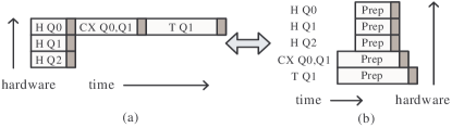
Figure 1a shows a possible execution of a simple series of quantum gates involving qubits Q0, Q1 and Q2. Each gate involves some encoded ancilla preparation for the QEC step which must follow it. In addition, some gates, called non-transversal gates, require further encoded ancilla preparation simply to be performed (elaborated upon in Section 2.4). Figure 1b shows these operations performed at the speed of data. Chi et al. suggest that these ancilla preparation operations could be done in advance, but the hardware cost for this parallelization grows quickly as the critical path is shortened.
In Section 2, we investigate quantum circuits for encoded ancilla preparation and evaluate them in terms of error and complexity. In Section 3, we identify three common subcircuits of larger quantum algorithms and evaluate their characteristics concerning encoded ancilla needs for both QEC and non-transversal gates. In Section 4, we detail the layout and throughput of a pipelined ancilla factory specialized for generating encoded ancilla qubits. In Section 5, we combine our analyses to answer the overall question of the feasibility of running a quantum circuit at the speed of data, and we conclude in Section 6.
2 Ancilla Preparation Circuits
Typical quantum circuits require many encoded ancilla qubits. In this section, we discuss several ancilla preparation circuits and evaluate them in terms of complexity and error. Ultimately, we select encoding circuits that will be used in our layouts in Section 4.
2.1 Computing on Encoded Data Bits

Since quantum data is very fragile, it must be encoded at all times in an appropriate quantum error correction code. A high-level view of the procedure for error-correcting an encoded data qubit is shown in Figure 2. Both the bit value and phase must be repaired during the QEC step [6]. Two sets of physical ancilla qubits are each encoded into the zero state and then consumed during correction.
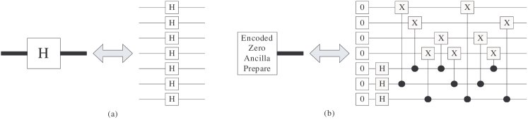
Gates applied to encoded data may be classified into two types: transversal and non-transversal. A transversal encoded gate is applied by performing the corresponding physical gate independently on each of the qubits comprising the encoded qubit, as shown in Figure 3a for the Hadamard gate. A non-transversal encoded gate is decomposed into a more complex set of physical operations, including multi-qubit physical operations between physical qubits within the same encoded qubit; for example, see the Basic Encoded Zero Ancilla Prepare in Figure 3b. Since errors are propagated between physical qubits during the application of non-transversal gates, such gates must be designed carefully to avoid introducing uncorrectable errors.
A class of quantum codes known as CSS codes [7, 3] allow transversal implementations of most encoded gates. For this reason, CSS codes are used in most analyses of the fault tolerance of quantum circuits. For the rest of this paper, we use the [[7,1,3]] CSS code [7]. Encoded gates that can be performed transversally on this code include the two-qubit CX, as well as the one-qubit X, Y, Z, Phase, and Hadamard gates. In order to have a universal gate set, we also need the non-transversal gate and the encoding procedure to create an encoded ancilla. We will discuss how to obtain a fault tolerant version of the gate later in this section, but first we investigate the problem of getting a fault tolerant encoding procedure.
2.2 Circuit Evaluation Methodology
Since encoded ancillae are a major component of error correction, it is critical to generate clean ancillae to avoid introducing errors during the correcting process. In the following, we will evaluate circuits by using the tools in [8] which allow us to lay out circuits. The effects of error are then modeled by Monte Carlo simulation where errors can be introduced at any gate or qubit movement operation. Additionally, we model the fact that two-qubit gates propagate bit and phase flips between qubits. This simulation is similar to what was done in [4] except with the addition of qubit movement error from our detailed layout. We assume an independent error probability for each gate and movement operation. The gate error rate is and the error per movement op is . Our gate and movement error rates are consistent with [9].
2.3 Encoded Ancilla Preparation
Since the Bit Correct and Phase Correct circuits in Figure 2 are fully transversal (each consisting of a transversal CX, measure and conditional correct [10]), we focus on the basic zero ancilla preparation circuit, shown in Figure 3b. The probability of an uncorrectable error in the resulting encoded output of this circuit is based on our evaluation methodology above. We would like to improve on this basic result.
There are two different circuit-level techniques for removing general errors from an encoded qubit: verification and correction. Verification tests a qubit in a known state for error and discards it if too much error is found. Correction is more complex, but it corrects a bit or phase error from an encoded qubit in an unknown state, thus it is more suitable for data qubits in a long-running computation. Encoded zero ancillae are in known state and may be discarded if necessary, so either method is suitable.
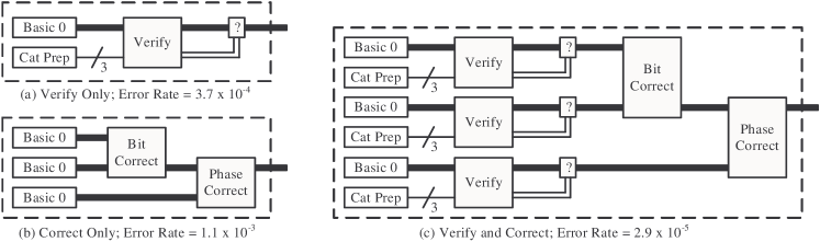
While Figure 3b shows the circuit for preparing an encoded ancilla in the zero state in the [[7,1,3]] CSS code, we would like a more error-free ancilla qubit for interaction with data. Figure 4 shows some example zero ancilla preparation circuits from the literature [11, 10], with the overall error rate for each given under the circuit. Correction alone (Figure 4b) loses to verification alone (Figure 4a) in both error and area. When comparing Figures 4a and 4c, it is important to note that they are not to scale. The “Basic 0” module (expanded in Figure 3b) is by far the most complex, so by doing both verification and correction, we get more than an order of magnitude improvement in error over verification alone for slightly more than three times the area. Thus, we shall use the circuit in Figure 4c in this paper.
Since we are using qubit verification as part of our encoded zero preparation, we need to know the success rate of verification. Using the same Monte Carlo simulation used for error probability calculations, we estimate the verification failure rate of the subunit 4a to be 0.2%. We will use this in calculations later in Section 4.4.
2.4 Fault Tolerant Gate
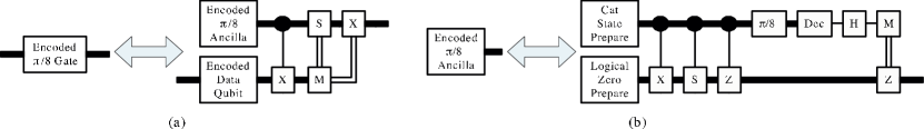
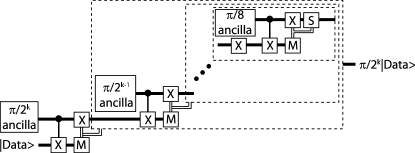
It has been shown that no quantum error correcting code has transversal gate implementations for all the gates in a universal set [12], and indeed, in the [[7,1,3]] CSS code, we need the non-transversal gate in order to complete the universal set. In order to maintain fault tolerance when performing the gate on a [[7,1,3]] encoded qubit, we use a technique developed in [13]. Their approach is to generate an encoded ancilla qubit encoded in the state and perform transversal interactions with the data, as shown in Figure 5a, to achieve the overall effect of an encoded gate.
To encode the ancilla qubit, we could try to create a physical ancilla qubit and then use the encoding circuit in Figure 3b, but this would result in errors on the original physical qubit propagating to each physical qubit in the final encoded ancilla, which is unacceptable. Thus, we require the far more complicated circuit shown Figure 5b, which consists of an encoded zero ancilla prepare, a 7-qubit cat state prepare (where a cat state is a specially prepared multi-qubit state) and a series of transversal encoded gates.
2.5 Fault Tolerant Gates
The Quantum Fourier Transform (QFT) requires controlled phase rotation gates by small angles (these gates replace the explicit tracking of roots of unity in the classical FFT algorithm). The amount of precision for these gates scales exponentially in the number of bits involved in the QFT [6]. A controlled phase rotation by can be generated by a CX gate and 3 single qubit gates [14]. Thus, using circuit techniques mentioned so far, we can implement every gate in the QFT fault tolerantly except these single qubit rotation gates. There are two problems with implementing an arbitrary precision phase rotation fault tolerantly:
-
•
For angles smaller than , there is no transversal gate implementation using the [[7,1,3]] code [12]. In fact, this seems likely to be true for all codes.
-
•
Such a gate would require the physical implementation of an arbitrary precision rotation – a difficult burden on the engineers of these devices.
Due to the above reasons, we adopt a technique by Fowler [14]. To approximate small angle rotations, we exhaustively search all permutations of T and H gates to find a minimum length sequence for a rotation gate up to an acceptable error.
We also note that if a physical gate is available in a given technology, an exact fault-tolerant can be implemented as shown in Figure 6. In order to be conservative about the availability of arbitrary precision rotation gates, we do not use this construction in the circuits in this paper. However, in Section 4.4.2, we briefly analyze the performance advantages of this technique.
3 Circuit Characteristics
We now characterize the runtime properties of some commonly used quantum circuits, focusing on the impact of encoded ancilla generation. Many quantum algorithms require ancillae to assist in computation. For example, an -bit Quantum Ripple-Carry Adder uses two -bit data inputs plus ancillae. In addition to this, shorter-lived ancillae are needed for QEC and for performing non-transversal encoded gates, as discussed earlier.
Throughout this paper we refer to the longer-lived ancillae used in the main computation as “data ancillae” and to the shorter-lived ones as “ancillae.” We make this distinction because data ancillae tend to have long enough lifespans that “discarding” them and restarting their portion of the computation has a relatively high cost. Our work focuses on the short-lived ancillae which need to be produced in large quantities and which may more easily be discarded and re-encoded.
| Physical | Latency | Latency |
|---|---|---|
| Operation | Symbol | (s) |
| One-Qubit Gate | 1 | |
| Two-Qubit Gate | 10 | |
| Measurement | 50 | |
| Zero Prepare | 51 |
We do most of our analysis in a symbolic fashion so that it may be applied to varying technologies and assumptions. However, we will also be applying the analysis to a specific technology, trapped ions [17], in order to make the results of our calculations more concrete. We use the physical gate latencies shown in Table 1, the [[7,1,3]] CSS code introduced in Section 2.1 and the encoded ancilla preparation circuits shown in Figures 4c and 5b. Note that the “Zero Prepare” in Table 1 refers to a physical zero prepare, which is the leftmost set of gates in the Basic Encoded Zero Ancilla Prepare in Figure 3b.
3.1 Benchmarks
For our benchmarks, we use the 32-bit Quantum Ripple-Carry Adder (QRCA) circuit from [18], the 32-bit Quantum Carry-Lookahead Adder (QCLA) circuit from [19] and a 32-bit Quantum Fourier Transform (QFT) circuit we derived using methodology described in Section 2.5. All three are core kernels of a varied array of quantum algorithms, including Shor’s factorization algorithm.
3.2 QEC Circuit Characteristics
We study our benchmark circuits at two extremes of the latency-area trade-off: 1) No overlap of QEC and computation (high latency, but low area), and 2) infinitely fast encoded ancilla production, resulting in an execution limited only by data dependencies (low latency, but potentially much higher area for encoded ancilla generation).
| Data Op Latency (s) | Data QEC Interact Latency (s) | Ancilla Prep Latency (s) | |
|---|---|---|---|
| Circuit | (% of total) | (% of total) | (% of total) |
| 32-Bit QRCA | 29508 (5.2%) | 95641 (16.7%) | 447726 (78.2%) |
| 32-Bit QCLA | 3827 (5.3%) | 11921 (16.7%) | 55806 (78.0%) |
| 32-Bit QFT | 77057 (5.0%) | 365792 (23.7%) | 1097376 (71.2%) |


Table 2 shows for each benchmark the latency of the critical path in the absence of movement (Column 2), as well as latencies for the data-dependent and data-independent (Columns 3 and 4) portions of QEC steps, assuming a QEC operation must be performed after each useful gate. The minimal running time is the sum of Columns 2 and 3, since these involve data qubits. Column 4 corresponds to encoded ancilla generation time. Clearly, there is much to be gained in overall execution time by taking ancilla preparation off the critical path.
| Avg Zero Ancilla | Avg Ancilla | |
|---|---|---|
| Bandwidth Needed | Bandwidth Needed | |
| Circuit | For QEC | For Gates |
| 32-Bit QRCA | 34.8 | 7.0 |
| 32-Bit QCLA | 306.1 | 62.7 |
| 32-Bit QFT | 36.8 | 8.6 |
Figure 7 shows for the QRCA (left), QCLA (middle) and QFT (right) the number of encoded ancillae used for QEC which need to be in the system as execution progresses in order to keep the circuit operating at the speed of data. This means that adequate hardware resources exist to generate and distribute the needed ancillae in time, but the interaction with data during each QEC step is still on the critical path of execution. Table 3 summarizes this figure by giving the average encoded ancilla bandwidth necessary for each.


These averages do not take into account the handling of peak periods. In reality, the encoded ancilla bandwidth necessary to run a circuit optimally may be higher than the average bandwidth. Figure 8 shows for the QRCA (left), QCLA (middle) and QFT (right) the circuit execution time assuming a steady throughput of encoded ancillae being generated, as specified on the x-axis. These graphs show us the sustained ancilla bandwidth necessary to run each circuit at near-optimal speed, but these are only estimates since they lack the details of movement and layout. In Section 4, we examine the associated hardware needs.
3.3 Non-Transversal One-Qubit Gates
The encoded ancilla bandwidth needs discussed in Section 3.2 for our three benchmarks include only zero ancillae needed for error correction. Non-transversal one-qubit gates account for 40.5%, 41.0% and 46.9% of our QRCA, QCLA and QFT benchmarks circuits, respectively, when using the [[7,1,3]] encoding. As explained in Section 2.4, the execution of a non-transversal encoded gate is performed with the use of a encoded ancilla qubit. Column 3 in Table 3 shows the corresponding ancilla bandwidth needed for each benchmark to achieve a runtime limited only by the speed of data (the sum of Columns 2 and 3 in Table 2).
4 Ancilla Factory Layout
In this section, we shall explore the design space of possible ancilla factories and determine the hardware resources necessary to produce encoded ancillae at the bandwidths calculated in Sections 3.2 and 3.3 in order to take ancilla generation off the critical path of execution.
4.1 Ion Trap Abstraction
Our area calculations are done using an abstraction of ion trap technology [17], described here.
Qubits:
A single qubit capable of holding one bit of quantum state is an ion. The physical implementation of a qubit is actually more complicated, but for our purposes, we may represent each qubit as a single ion.
Movement:
Electrodes are used to create potential wells in which qubits (ions) are trapped. Potential wells and the ions within are moved via an application of precise pulse sequences to the electrodes. Moving an ion around a corner takes more time than moving straight [20]. The latency numbers we use are shown Table 4.
Gates:
A gate is performed by firing precise laser pulses at a trapped ion. We may abstract away the physics and consider that a gate is performed by arrival at certain special “gate locations” in the layout.
Macroblocks:
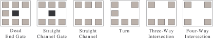
Since qubit movement is performed by electrodes whose position is fixed at fab time, certain “channels” for qubit movement are also set at fab time. The details of electrode structure are still evolving, so determining area in terms of number of ion traps is a bit ambiguous. For this reason, we use the macroblocks shown in Figure 9 as the basic building blocks of our layouts. Each macroblock has one or more “ports” through which qubits may enter and exit and which connect to an adjacent macroblock. To perform a gate operation, all involved qubits must enter a valid gate location (a black square in our macroblocks) and remain there for the duration of the gate. Our area numbers are all calculated in terms of macroblock count.
4.2 Data Qubit Area
Over the run of a quantum circuit, encoded data must perform four distinct types of operations: transversal one-qubit gates, non-transversal one-qubit gates, transversal two-qubit gates and QEC steps. As described in Section 2.4, a non-transversal one-qubit gate may be performed by preparing a specific encoded ancilla and interacting it transversally with the data qubit. Likewise, the data/ancilla interaction portion of a QEC step involves a transversal two-qubit gate. In the end, the main operations the encoded data must support are transversal one- and two-qubit gates.

To support these major operations, we use single compute regions as shown in Figure 10. The design consists of a single column of Straight Channel Gate Macroblocks with enough room for a single encoded qubit (seven macroblocks for the [[7,1,3]] CSS code), with access on either side to whatever interconnect network is being used. Thus, if we are encoding each qubit into physical qubits, the total area used by data is , where is the total number of data qubits (including data ancillae) in the circuit.
4.3 Simple Ancilla Factories

We now focus on designing an ancilla factory, a concept first proposed in [21]. An ancilla factory is a portion of the layout which consumes stateless physical ancillae and produces a steady stream of encoded ancillae at some rate. Figure 11 shows a simple ancilla factory to execute the circuit in Figure 4c. Each row of gates has room for ten physical qubits, seven to be encoded and three for verification. The adjacent rows are used for communicating. When all three are encoded and verified, the middle one is bit-corrected by the top one and phase-corrected by the bottom one. Using a hand-optimized schedule, the total latency of a single ancilla preparation is approximately: .
Substituting in the ion trap latencies in Tables 1 and 4, the layout in Figure 11 has a total latency of 323s with a throughput of 3.1 encoded ancillae per millisecond and an area of 90 macroblocks. Using this simple ancilla factory, we could produce any desired bandwidth of encoded ancillae by replicating the layout as many times as necessary. Unfortunately this design is inefficient in that the verification qubits needlessly take up space during the seven-qubit zero encoding procedure. To combat this inefficiency we instead consider a pipelined approach.
4.4 Pipelined Ancilla Factories
Classically, pipelining a circuit is done by inserting synchronization points (registers) into the circuit’s datapath to enable logic reuse, thereby increasing throughput with a small increase in latency. We can apply a similar technique to our ancilla factory layout in an effort to improve area utilization. Due to the precise electrode and laser pulse sequences needed to implement movement and gates, ion trap layouts are by definition synchronous without additional synchronization elements. Instead, we must add a set of communication channels between pipeline stages allowing qubit movement for maximum gate location occupancy.

4.4.1 Encoded Zero Ancilla Factory
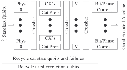
We consider the entire circuit for fault tolerant encoded zero ancilla creation (Figure 4c). Figure 12 shows a fully pipelined microarchitecture for this circuit, which consists of four stages. Each stage contains a number of functional units for its subcircuit such that the output bandwidth of one stage is matched to the input bandwidth of the next. Adjacent stages are separated by a crossbar (Figure 13a), which consists of two vertical columns, fully connected horizontally, one for upwards movement, the other for downwards.
Stage 1 consists of preparing a junk physical qubit into the zero state with an optional Hadamard gate at a single gate location (Figure 13b). Even though only some of these qubits need the Hadamard, we group them all into the same set of functional units.
| Latency | BW (qubits/ms) | Area | ||||
|---|---|---|---|---|---|---|
| Functional Unit | Symbolic Latency | (s) | Stages | In | Out | |
| Zero Prep | 73 | 1 | 13.7 | 13.7 | 1 | |
| CX Stage | 95 | 3 | 221.1 | 221.1 | 28 | |
| Cat State Prep | 62 | 2 | 96.8 | 96.8 | 6 | |
| Verification | 82 | 1 | 122.0 | 85.2 | 10 | |
| B/P Correction | 138 | 1 | 152.2 | 50.7 | 21 | |
| Unit | Total | Total | |
|---|---|---|---|
| Functional Unit | Count | Height | Area |
| Zero Prepare | 24 | 24 | 24 |
| CX Stage | 1 | 4 | 28 |
| Cat State Prepare | 1 | 2 | 6 |
| Verification | 3 | 30 | 30 |
| B/P Correction | 2 | 42 | 42 |
Stage 2 consists of two types of units. Looking at the CX portion of the ancilla prepare circuit in Figure 3b, we see that the first three CX’s can be performed in parallel, as can the next three, followed by the final three. Thus, we may use the pipelined layout in Figure 13c for this functional unit, with three sets of qubits (each performing three CX’s with one idle qubit) in this functional unit at a time. The Cat Prep units (Figure 13d) create a three-qubit cat state out of three physical zero ancillae by performing two CX’s in succession.
Verification of the encoded zero ancillae using the cat states is performed in Stage 3 and involves performing three CX’s in parallel and then measuring the cat state qubits to determine success or failure of the encoded ancilla. Since the encoded ancilla qubits must wait for the measurement to complete, we need 10 macroblocks, one for each qubit as shown in Figure 13e. When this is done, the three qubits of the cat state are recycled immediately, as well as the other seven qubits if the verification failed.
Finally, in Stage 4, a verified encoded zero ancilla A is first bit-corrected by a verified encoded zero ancilla B and then phase-corrected by a verified encoded zero ancilla C. Since we need storage room for A plus room to measure both B and C in parallel (allowing us to overlap these measurements in time), each such functional unit needs space for three encoded ancillae, as shown in Figure 13f.
Table 5 summarizes the latency breakdown for each stage of the pipeline and provides numerical values for various characteristics of each functional unit under our ion trap assumptions. Note that Stages 3 and 4 have input bandwidth different from output bandwidth due to the fact that some qubits are used up and recycled in these stages. To achieve high resource utilization, we determine unit count by matching bandwidth between successive stages. The results are shown Table 6.
For the crossbars, we use a two-column design, one column for upwards movement, the other for downwards, in order to avoid congestion. However, physical qubits exiting Stage 1 are funneled inward to the much smaller Stage 2, so we use a single column crossbar since bi-directionality is likely unnecessary. The total crossbar area is thus 24 + 2 * 30 + 2 * 42 = 168 macroblocks, and the total functional unit area is 24 + 34 + 30 + 42 = 130 macroblocks, resulting in a total area of 298 macroblocks.
For overall throughput, we take the minimum throughput among the stages. The bottleneck in the factory is the CX Stage. Each seven physical qubits out of this stage correspond to an encoded zero ancilla. Approximately 99.8% of these qubits are successfully verified (using the results of our Monte Carlo simulations mentioned in Section 2.3), and two-thirds of them are then used to correct the other third. Thus, the overall throughput of our zero ancilla factory is: encoded ancillae / ms.
4.4.2 Encoded Ancilla Factory
In Section 3.3, we showed that a non-trivial supply of encoded ancillae are also needed by our circuits. The circuit in Figure 5b shows how to turn a zero ancilla generated by our pipelined ancilla factories into an encoded ancilla. This circuit may be divided into four stages: 1) Cat State Prepare, 2) Transversal Controlled-Z/S/X, plus Transversal , 3) Decode, 4) One-qubit H, One-qubit Measure, Transversal Z conditional on measurement.
| Stage | Symbolic Latency | Latency | In BW | Out BW | Area |
|---|---|---|---|---|---|
| Cat State Prepare | 218 | 32.1 | 32.1 | 12 | |
| Transversal CX/CS/CZ/ | 53 | 264.2 | 264.2 | 7 | |
| Decode (plus Store) | 218 | 64.2 | 36.7 | 19 | |
| H/M/Transversal Z | 74 | 108.1 | 94.6 | 8 |
Table 7 shows the characteristics of each of these stages. Note that bandwidths here are in physical qubits, which is why Stages 1 and 3 have differing bandwidths despite having the same latency. We now match bandwidths just as we did for the zero ancilla factory in order to get close to full utilization. Table 8 shows the the final unit counts of our ancilla factory. Note that only half the qubits consumed by Stage 2 come from Stage 1 (the others come from an encoded zero ancilla factory).
The total stage heights are different enough that an exact layout would likely require partially folding some stages into others and simulating execution to determine exact crossbar sizes needed to avoid congestion. For our purposes, we will allocate two columns to each crossbar, since qubits must be able to move in both directions at the same time. Thus, the total crossbar area is 2 * 24 + 2 * 52 + 2 * 52 = 256 macroblocks, and the total functional unit area is 48 + 7 + 76 + 16 = 147 macroblocks, resulting in a total area of 403 macroblocks. Note that this is only the area for turning an encoded zero into an encoded . This factory needs to be supplied by zero ancilla factories in order to function, which we account for in Section 5.
The bottleneck of this ancilla factory is the Cat State Prepare stage. Each seven-qubit cat state produced by this stage results in one encoded ancilla produced by the factory, so the throughput of the factory is equal to the throughput of this stage: 18.3 encoded /8 ancillae / ms.
As mentioned in Section 2.5, we build up smaller angle rotations from combinations of and H gates instead of building ancilla factories for them. It is worthwhile to note that if physical gates with adequate precision are available, the critical path for the data can be decreased further. From Figure 6 we see that the critical path for the data through such a factory would on average consist of CX gates and one fewer X gates.
| Unit | Total | Total | |
|---|---|---|---|
| Stage | Count | Height | Area |
| Cat State Prepare | 4 | 24 | 48 |
| Transversal CX/CS/CZ/ | 1 | 7 | 7 |
| Decode (plus Store) | 4 | 52 | 76 |
| H/M/Transversal Z | 2 | 16 | 16 |
5 Architectural Trade-offs
We now bring our analyses together to draw quantitative conclusions about running a quantum circuit at the speed of data and to compare against proposed architectures from prior work. Following that, we present a more qualitative discussion of some conclusions we’ve drawn from this work.
5.1 Matching Production to Need
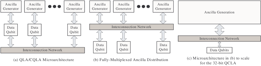
We divide the microarchitecture of a quantum layout into three components: 1) hardware resources for generation of encoded ancillae; 2) hardware resources for data operations, including operations involving data ancillae and the data/ancilla interaction portion of a QEC step; and 3) an interconnection network for moving around both encoded data and ancillae. Figure 14a shows the (C)QLA microarchitecture [22, 15] using these components, with each data qubit (whether in a compute region or memory) having an associated ancilla generation unit for QEC. Figure 14b shows an ancilla factory-based microarchitecture wherein encoded ancillae are being generated across the chip and distributed to data as need dictates.
| Encoded Ancilla | Data Area | QEC Ancilla Factories | Ancilla Factories | |
|---|---|---|---|---|
| Quantum Circuit | Bandwidth For QEC | (% of total) | Area (% of total) | Area (% of total) |
| 32-Bit QRCA | 34.8 | 679 (33.6%) | 986.9 (48.8%) | 354.7 (17.6%) |
| 32-Bit QCLA | 306.1 | 861 (6.8%) | 8682.2 (68.4%) | 3154.4 (24.8%) |
| 32-Bit QFT | 36.8 | 224 (13.2%) | 1043.5 (61.3%) | 433.7 (25.5%) |
Table 9 gives the relative areas of two of the three components of the microarchitecture in Figure 14b when running our benchmarks at (or near) the speed of data under our ion trap assumptions. We depict our microarchitectural components to scale for the 32-bit QCLA in Figure 14c. The encoded zero ancilla bandwidth for error correction is the average bandwidth required for each circuit (Table 3). A corresponding encoded ancilla bandwidth is computed (but not shown in the table) to run the circuit at that speed. Column 4 includes only those zero ancilla factories producing for QEC. Column 5 includes both encoding factories and sufficient encoded zero ancilla factories to supply the encoding factories.
We see that even the most serial of the benchmarks, the Quantum Ripple-Carry Adder, requires a substantial portion of the chip (two-thirds) dedicated to encoded ancilla generation in order to take this generation off the execution’s critical path, while the more parallel QCLA requires more than 90%.
5.2 Latency/Area Evaluation
The proposals for both QLA and CQLA specify space for only serial production of ancillae at each encoded data qubit location. We generalize this to GQLA and GCQLA in which we replicate the ancilla area at each data qubit to allow parallel production of ancillae. CQLA has additional flexibility in that different numbers of data units can be present in the compute cache. We wish to quantify the efficiency of ancilla production in each microarchitecture by studying area needed for a given execution time.
Methodology:
Using dataflow graphs of our benchmarks and the estimates in Tables 5-8, we implemented an event-based simulation of ancilla factory production and data qubit gate consumption. Simulation of the QLA [22] microarchitecture assumes that each data qubit in the computation has a dedicated cell with ancilla production. Data qubits are always moved back to their home base to do the error correction after each encoded gate. We simulate dataflow execution taking into account latency of the ancilla production and encoded gate execution, using latencies from Tables 5 and 7.
CQLA [15] optimizes the QLA design by adding a cache of data qubits that are in the current working set. To simulate this, we added tracking of which qubits are in the “compute cache” and account for cache miss and write-back latencies. This was the most complicated simulation and has an implementation similar to that of sim-cache in SimpleScalar [23]. We used the same basic ancilla production and data gate latencies as for QLA.


Results:
Figure 15 shows overall circuit execution time as a function of total area dedicated to ancilla factories (of both types) for the different microarchitectures being tested for QRCA (left), QCLA (middle) and QFT (right). Total data qubit area is given in the caption for each.
We notice that CQLA takes about half an order to an order of magnitude longer to execute than Fully-Multiplexed Ancilla Distribution. This is due to the incurrence of cache misses in CQLA, whereas Fully-Multiplexed always distributes encoded ancillae to data when necessary. CQLA also plateaus half an order to an order of magnitude higher than Fully-Multiplexed since, even with very fast encoded ancilla production, cached misses are still incurred to bring ancillae to data.
QLA requires two orders of magnitude more area for ancilla production to match execution time with Fully-Multiplexed, which is logical since many ancilla generators are idle much of the time in QLA when they could be used to feed nearby data need. On the other hand, QLA eventually plateaus at a similar execution time as Fully-Multiplexed, which makes sense since it has no concept of cache misses. QLA simply needs very high encoded ancilla production at each data qubit in order to run at the speed of data.
5.3 Qalypso: Microarchitectural Implications of Pipelined Ancilla Factories
The simple encoded zero ancilla factory in Figure 11 has an area of 90 macroblocks and a throughput of 3.1 encoded ancillae per millisecond. The pipelined encoded zero ancilla factory designed in Section 4.4 has an area of 298 macroblocks and a throughput of 10.5 encoded ancillae / ms. They produce virtually the same encoded zero ancilla bandwidth per unit area, thus seemingly negating some of the benefits of pipelining111This is a result of the facts that the technology is inherently synchronous and that individual gate locations are multi-purpose..
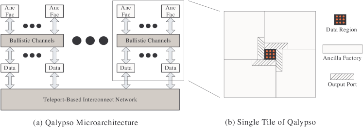
Nonetheless, we conclude that pipelined ancilla factories provide significant benefit in having concentrated input and output “ports.” We propose Qalypso, a tiled microarchitecture shown in Figure 16a using the tile shown in Figure 16b, with ballistic movement being used within a tile and teleportation of data between tiles [16]. The central data region consists of a dense packing of encoded data qubits and channels for local ballistic movement. The ancilla factories each have an output port physically near the data region so encoded ancillae do not have far to travel. This is beneficial both in reducing aggregate movement error on encoded ancillae and in avoiding congestion problems from having encoded ancillae generated uniformly throughout an ancilla factory. Meanwhile, since the limiting factor on move speed in ion traps is state decoherence rather than control of the electrodes, stateless qubits may be recycled to factory input ports much more quickly, allowing the input ports to be far from the data.
This architecture differs from (C)QLA in two significant respects. First, our data regions consist of data alone. In CQLA, the compute regions consist of both data and ancilla generation units, meaning that data are physically quite a bit further apart even within one compute region and generally require teleportation for movement. Even if QEC were performed as part of teleportation [24], this requires twice as many encoded ancillae as a straightforward QEC step. Thus, we suggest that our data regions be made as large as possible to allow data qubits to reach each other using ballistic movement instead of teleportation as much as possible. Though ballistic movement is somewhat error prone, the area of a data region consisting of nothing but encoded data qubits is still quite small, so teleportation is only necessary between data regions.
Second, ancilla factories surrounding a data region in our design are shared by all data qubits within that region. In Figure 14a, which represents the (C)QLA microarchitecture, each ancilla generator is dedicated to a single data qubit (location), so imbalances in encoded ancilla need cause some generators to go idle while others cannot meet need. By having a full crossbar between generators and consumers (data qubits), as in Figure 14b, fresh ancillae go where they are needed within a single data region.
The choice of data region size is still an open problem and depends on the level of parallelism in the target application. The determining factors will likely be local movement congestion within the data region and load on the inter-tile interconnect, which are shown as the grey boxes in Figure 16a. Analyses concerning these trade-offs will be the subject of future research.
6 Conclusion
We find that ancilla generation bandwidth in a quantum computer is the primary performance bottleneck, and we present a microarchitecture that takes this bottleneck off the critical path. We examine two major consumers of ancillae: quantum error correction (QEC) and non-traversal quantum gates, such as the gate for the [[7,1,3]] CSS code. We characterize our benchmarks to find bandwidth needs ranging from 30 to 300 encoded zero ancillae / ms and ranging from 7 to 60 encoded ancillae / ms for ion trap quantum computers.
Our resulting microarchitecture, Qalypso, is optimized for ancilla generation and distribution, featuring dense data-only regions fed by nearby ancilla factories. We present layouts for these ancilla factories and show that ancilla generation takes the majority of the chip area even in the most serial of our circuits, the ripple-carry adder. As an interesting aside, we find that pipelining does not have the same beneficial impact on throughput as in classical circuits but does provide an important structural benefit: it can produce high bandwidth ancillae directed at a single output port. Qalypso can produce circuits of similar speed to previous architectures with greatly reduced resources or alternatively can produce circuits of much greater speed than previous architectures for similar area.
References
- [1] P.W. Shor. Scheme for reducing decoherence in quantum computer memory. Phys. Rev. A, 52(4):2493, 1995.
- [2] C. Zalka. Simulating quantum systems on a quantum computer. Proceedings: Mathematical, Physical and Engineering Sciences, 454(1969):313–322, 1998.
- [3] AR Calderbank and P.W. Shor. Good quantum error-correcting codes exist. Phys. Rev. A, 54(2):1098, 1996.
- [4] A.M. Steane. Overhead and noise threshold of fault-tolerant quantum error correction. Phys. Rev. A, 68(4):42322, 2003.
- [5] E. Chi, S.A. Lyon, and M. Martonosi. Tailoring quantum architectures to implementation style: a quantum computer for mobile and persistent qubits. ISCA-34, pages 198–209, 2007.
- [6] M.A. Nielsen and I.L. Chuang. Quantum computation and quantum information. Cambridge Univ. Press, 2000.
- [7] A. Steane. Multiple-Particle Interference And Quantum Error Correction. Proceedings- Royal Society. Mathematical and physical sciences, 452(1954):2551–2577, 1996.
- [8] M. Whitney, N. Isailovic, Y. Patel, and J. Kubiatowicz. Automated Generation of Layout and Control for Quantum Circuits. In Proc. of ACM Intl. Conf. on Computing Frontiers, 2007.
- [9] A.M. Steane. How to build a 300 bit, 1 Gop quantum computer. Arxiv preprint quant-ph/0412165, 2004.
- [10] J. Preskill. Fault-tolerant quantum computation. Arxiv preprint quant-ph/9712048, 1997.
- [11] K.M. Svore, D.P. DiVincenzo, and B.M. Terhal. Noise Threshold for a Fault-Tolerant Two-Dimensional Lattice Architecture. Arxiv preprint quant-ph/0604090, 2006.
- [12] B. Zeng, A. Cross, and I.L. Chuang. Transversality versus Universality for Additive Quantum Codes. eprint arXiv: 0706.1382, 2007.
- [13] X. Zhou et al. Methodology for quantum logic gate construction. Phys. Rev. A, 62(5):52316, 2000.
- [14] A.G. Fowler. Towards Large-Scale Quantum Computation. Arxiv preprint quant-ph/0506126, 2005.
- [15] D.D. Thaker, T.S. Metodi, A.W. Cross, I.L. Chuang, and F.T. Chong. Quantum Memory Hierarchies: Efficient Designs to Match Available Parallelism in Quantum Computing. ISCA-33, 2006.
- [16] N. Isailovic, Y. Patel, M. Whitney, and J. Kubiatowicz. Interconnection Networks for Scalable Quantum Computers. ISCA-33, 2006.
- [17] S. Seidelin et al. Microfabricated surface-electrode ion trap for scalable quantum information processing. Phys. Rev. Lett., 96(25):253003, Jun 2006.
- [18] T.G. Draper. Addition on a Quantum Computer. Arxiv preprint quant-ph/0008033, 2000.
- [19] T.G. Draper, S.A. Kutin, E.M. Rains, and K.M. Svore. A logarithmic-depth quantum carry-lookahead adder. Arxiv preprint quant-ph/0406142, 2004.
- [20] WK Hensinger, S. Olmschenk, D. Stick, D. Hucul, M. Yeo, M. Acton, L. Deslauriers, et al. T-junction ion trap array for two-dimensional ion shuttling, storage, and manipulation. Appl. Phys. Let., 88:034101, 2006.
- [21] A.M. Steane. Space, Time, Parallelism and Noise Requirements for Reliable Quantum Computing. Quantum Computing: Where Do We Want to Go Tomorrow?, 1999.
- [22] T.S. Metodi, D.D. Thaker, A.W. Cross, F. Chong, and I. Chuang. A Quantum Logic Array Microarchitecture: Scalable Quantum Data Movement and Computation. MICRO-38, 2005.
- [23] D.C. Burger, T.M. Austin, and S. Bennett. Evaluating Future Microprocessors: The SimpleScalar Tool Set. University of Wisconsin-Madison, Computer Sciences Dept, 1996.
- [24] C.H. Bennett, D.P. DiVincenzo, J.A. Smolin, and W.K. Wootters. Mixed-state entanglement and quantum error correction. Physical Review A, 54(5):3824–3851, 1996.