Oersted fields and current density profiles in spin-torque driven magnetization dynamics – Finite element modelling of realistic geometries
Abstract
The classical impact of electrical currents on magnetic nanostructures is analyzed with numerical calculations of current-density distributions and Oersted fields in typical contact geometries. For the Oersted field calculation, a hybrid finite element / boundary element method (FEM/BEM) technique is presented which can be applied to samples of arbitrary shape. Based on the FEM/BEM analysis, it is argued that reliable micromagnetic simulations on spin-tranfer-torque driven magnetization processes should include precise calculations of the Oersted field, particularly in the case of pillar contact geometries. Similarly, finite-element simulations demonstrate that numerical calculations of current-density distributions are required, e.g., in the case of magnetic strips with an indentation. Such strips are frequently used for the design of devices based on current-driven domain-wall motion. A dramatic increase of the current density is found at the apex of the notch, which is expected to strongly affect the magnetization processes in such strips.
pacs:
85.75.-d, 75.40.Mg, 41.20.-q, 41.20.GzI Introduction
Current-driven magnetization processes have recently evolved to probably the most active field in magnetism. Recent discoveries demonstrating that, by exploiting the electron spin, the magnetization state of a nanomagnet could be influenced directly by electrical currents instead of external magnetic fields Kiselev03 ; Rippard04 ; Tsoi03 ; Vernier04 have given rise to numerous extensive studies on the spin-transfer torque (STT) effect. Magnetization dynamics induced by STT Slonc96 ; Berger96 is attractive for both technological aspects and fundamental physics. Unlike the field-induced magnetic switching, which in the case of nanodevices is connected with the technological difficulty of focussing magnetic fields on very small length scales, the STT effect provides the possibility to switch, e.g., individual magnetic nanoelements in integrated circuits or in densely packed arrays Liu07 . Moreover, the current-induced magnetization dynamics differs qualitatively from the field-induced dynamics. A striking example thereof is the excitation of high-frequency magnetic oscillations induced by means of DC spin-polarized currents Kiselev03 ; Rippard04 ; an effect without analogy in the field-driven dynamics. The further possibility of tuning the frequency of these oscillations by varying the current strength bears a high potential for future applications.
The STT effect and the related fascinating features of current-induced magnetization dynamics have been extensively studied by various groups over the last years. Micromagnetic simulations have nowadays developed to such a high level of accuracy and reliability that they provide an important tool for the design and for the understanding of magnetic nanostructures and their magnetic properties. While the STT effect has been implemented in several micromagnetic codes Berkov06 ; Lopez05 ; LeeDeac04 , there is often still a quantitative discrepancy between simulated and experimental results in the case of current-induced magnetization dynamics BerkovMiltat07 . This differs from the static Cherifi05 ; Hertel05 and the field-driven cases Buess04 , where countless examples can be found showing excellent agreement between experiment and simulation, thereby demonstrating the predictive power of classical micromagnetic simulations.
One of the possible sources for such disagreement is connected with the Oersted field. Current-induced magnetization processes require high current densities, typically larger than about 1011 A/m2. Such current densities are inevitably connected with sizable magnetic fields, known as Oersted or Ampère fields Jackson99 . In addition to the usual external and internal effective fields entering the Landau-Lifshitz-Gilbert equation of motion, and in addition to the STT term, these Oersted field also affect the magnetization. The importance of the Oersted field in spin-transfer induced magnetic switching process has recently been pointed out by various groups Stoehr06 ; Devolder07 . In view of the aforementioned high accuracy of classical micromagnetic simulations, a numerical method is required in order to calculate the Oersted field contribution with high precision when STT effects are studied. In this article a method based on a combination of the finite-element method (FEM) and the boundary element method (BEM) is presented which allows for fast and precise calculations of the Oersted field in arbitrary contact geometries. The hybrid FEM/BEM scheme has several advantageous features, including the simple consideration of inter-particle interactions resulting from Oersted fields generated, e.g., in complex nanocircuits Parkin04 or arrays of current-carrying nanopillars Kaka05 .
The paper is structured as follows. First, the basic equations and the numerical method for the Oersted field calculation are peresented. Subsequently, in section IV a method to calculate current-density distributions in non-trivial geometries is outlined. Finally, a few examples on the application of these methods to structures that are currently used for intensive studies on current-driven magnetization processes are presented in section V.
II Basic equations
Consider a current-carrying sample of known size and shape. Let us further assume that the current density distribution is known for every point in the volume of sample. The calculation of will be discussed in in section IV. The Oersted field connected with a current density distribution can be obtained by direct integration over the volume of the current-carrying particle:
| (1) | |||||
| (2) |
where
| (3) |
is Green’s function with
| (4) |
and is the Dirac delta function. Note that . If the volume of the sample is discretized into finite elements, it is relatively simple to perform such a numerical integration. However, the direct integration according to eq. (1) has a number of disadvantages from a numerical point of view. The volume integration over Green’s function may give rise to serious problems of accuracy: Simple integration schemes can lead to inaccurate results because the value of Green’s function can vary significantly within a single finite element containing a point if the viewpoint is close to that element. Moreover, the computational effort involved with this direct integration is very large: The calculation of each component of at a single point requires an integration over the whole volume of the conductor. A more convenient approach in terms of accuracy and efficiency consists in numerically solving partial differential equations instead of the direct integration according to eq. (1). In the following, the basic steps for a FEM/BEM formulation of the Oersted field problem are outlined.
The fundamental equation for the calculation of Oersted fields is Ampère’s law:
| (5) |
In a current-carrying ferromagnet with magnetization , the magnetostatic field is constituted by two parts:
| (6) |
where is the demagnetizing field (also called dipolar field of stray field) created by the magnetic surface and volume charges, and the field is the magnetic Oersted field (also called Ampère field) due to the current density . The following equations apply to these two static magnetic field contributions:
| (7) | |||||
| (8) |
The calculation of is one of the central parts of any micromagnetic code. Several powerful methods have been discussed for the numerical calculation of the dipolar field Chen97 ; Yuan92 and this part of the problem can now be generally considered as solved. Due to its similarity with the method described later, one particular efficient method to calculate the demagnetizing field should be pointed out here, namely the hybrid FEM/BEM algorithm presented by Koehler and Fredkin Koehler90 . Henceforth, only the contribution from the electric current shall be considerd, and the subscript “c” is omitted for simplicity.
| (9) |
In the region outside the conductor, the source term is zero, i.e.,
| (10) |
Thus, each component of satisfies an equation of the Poisson form inside the conductor and of the Laplace form on the outside. Equations (9) and (10) describe an open boundary problem. Such problems are characterized by the absence of well-defined boundary conditions at the sample surface. The solution is uniquely defined by the condition of “regularity at infinity”, i.e., a Dirichlet-type of boundary condition for :
| (11) |
A possible approach for the consideration of such boundary conditions consists in attempting to expand the computational region to “infinity”, e.g. by applying bijective transformations to map the infinite volume surrounding the sample onto a volume of finite size, which can then be discretized with finite elements Brunotte92 . Such transformation methods can suffer from accuracy problems because the discretized spatial transform effectively corresponds to a truncation of the computational region at more or less large distances. Moreover, these methods require the external region to be free of charges, thereby precluding the possibility of calculating the field in the case of interacting current carriers. An alternative approach, which solves these problems, is the use of a hybrid finite element / boundary element method. In the boundary element method, the fundamental solution of a partial differential equation is used. In this case, the fundamental solution is given by Green’s function, which automatically fulfils the boundary condition at infinity.
III Hybrid FEM/BEM formulation
The first step in developing the FEM/BEM formulation consists in an analysis of the properties of the solution at the sample boundary. From eq. (9) a jump condition for the normal derivative of at the boundary of the current carrier is easy to derive:
| (12) |
This equation correspondingly holds also for the and components of . In eq. (12) is the unit vector along the axis and is the surface unit vector directed outwards. Note that this condition represents a discontinuity of the gradient of at the boundary. However, it does not provide any information on the value of the inward limit of the gradient of . This condition can therefore not be used directly as a Neumann boundary condition at the boundary as it would be required for a unique solution of the differential equation in the region .
In order to obtain useful boundary conditions at the sample surface, the Oersted field can be split in two parts, . These fields shall have the following properties: (i): Outside the current carrier, the part is zero. (ii): The part satisfies Poisson’s equation
| (13) |
with Neumann boundary conditions
| (14) |
(iii): The part satisfies the Laplace equation
| (15) |
and its derivatives are continuous along the boundary.
The boundary conditions required for the solution of eq. (15) will be discussed later. The jump condition for the individual components and at the boundary
| (16) |
results from the condition that the field must be continuos at the surface.
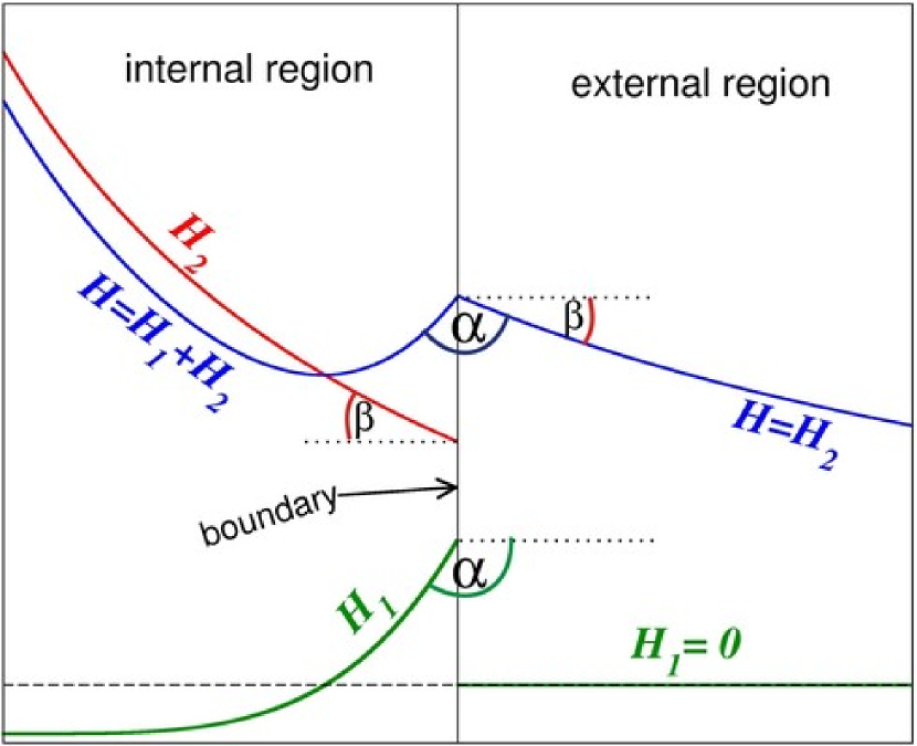
The splitting of the field in two parts is schematically shown in Fig. 1. The advantage of this splitting is that it is possible to extract useful boundary conditions required for the solution of Poisson’s equation: By setting to zero outside the sample, the discontinuity condition (12) is converted into a Neumann boundary condition (14) that can be used to solve eq. (13). With the finite element method, it is relatively easy to solve the Poisson equation (13) with given Neumann boundary conditions (14). After that, the somewhat more complicate part needs to be addressed, i.e., finding the values of at the particle surface. These values will provide the Dirichlet boundary conditions required for the solution of Laplace’s equation (15). For this task, the boundary element method is used.
Multiplying eq. (4) with and eq. (13) with yields, after subtraction and integration over the volume of the region :
which, by virtue of Green’s theorem, transforms into
The surface integrals extend over the boundary of the region , i.e., the sample surface. Inserting the boundary condition for
| (18) |
the equation simplifies to
| (19) |
The last term can be identified as the right-hand side of eq. (1), yielding
| (20) |
The integral is trivial as long as the point is located inside or outside the volume . The situation requires more attention when is a point on the boundary. In this case, the inward limit is taken by introducing an infinitesimal distance of the point (located in the internal region) to the surface. The resulting integral over the delta function is in this case
| (21) |
where is the solid angle subtended at the boundary point .
Hence, an equation is obtained with which can be calculated at each boundary point:
| (22) |
Accurate numerical methods to perform this integral by means of BEM are discussed in Ref. Lindholm84 . In principle, eq. (20) would be sufficient to calculate at any point inside (and outside) the volume, so that the resulting total field could be calculated at any discretization point. However, the calculation of at one point requires in this case an integration over the whole surface. This approach would thus have similar disadvantages as the direct integration according to eq. (1). By using equation (22) instead, we obtain at relatively low cost the boundary values of . Having these Dirichlet boundary conditions, it is easy to solve eq. (15) in the volume by means of the FEM.
It is noteworthy that eq. (22) has the same form as it has been used in the FEM/BEM scheme described in Ref. Koehler90 to calculate the scalar magnetic potential of a ferromagnet. From the viewpoint of implementation into a program, this means that the matrix required for the numerical calculation the values of according to eq. (22) is already available in the micromagnetic code if the FEM/BEM scheme presented in Ref. Koehler90 is used for the calculation of the magnetic scalar potential.
IV Calculation of current density distributions
Unless the geometry of the current-carrying sample is trivial, the current density distribution needs to be determined numerically prior to the calculation of the Oersted field. The starting point for the calculation of the current density distribution is Ohm’s law
| (23) |
is the local electric field and the conductivity is assumed to be a scalar. The electric field is the gradient field of the electrostatic potential , so that . Charge conservation yields and thus , which ultimately leads to
| (24) |
This equation has the form of the stationary diffusion equation and converts into the Laplace equation for if is homogeneous.
Elliptic differential equations of the type (24) are routinely solved numerically with FEM. However, appropriate boundary conditions must be specified to obtain a unique solution. In this case, the boundary conditions are given by the fact that the current is not flowing perpendicular to the sample surface except for the leads, where a known current density is entering and leaving the sample. In the case of two contact leads of the same size, the boundary condition is at the leads, leading to
| (25) |
In a more general case, only the value of the total current flowing through the sample is known. The value of the current density at the positive and negative leads then needs to be determined by dividing the total current flowing through each lead by the area of the contact region. Note that eq. (24) with given Neumann boundary conditions is as easy to solve numerically for homogeneous conductivity as it is in the case of inhomogeneous conductivity .
The method described here for the calculation of current density distributions is generally well known and has been applied in various previous publications Moussa01 ; Holz03 ; Sarau07 . It is included in this manuscript mainly for completeness, because such current density distribution calculations usually are a necessary prerequisite for the calculation of Oersted fields.
V Examples
The methods outlined above can be applied to various problems which are of high importance for modern research topics in the field of nanomagnetism. In this section, a few examples are presented. These include the current density distribution in a thin strip with an indentation (“notch”) and the calculation of the current density distribution and of the Oersted field in a pillar contact geometry as it is used to study high-frequency excitations in nanomagnets Kiselev03 ; Dassow06 .
V.1 Current density distribution in a thin strip with a notch
Ferromagnetic thin strips with width in the sub-m range and thicknesses of the order of a few ten nm have attracted much interest over the past years. One reason is the particular type of head-to-head domain walls that occur in such structures McMichael97b . Magnetic strips have been proposed to be used in future nanomagnetic devices, in which the head-to-head domain walls would serve as units of information that could be processed in logical devices Parkin08 ; Allwood02 . It has further been shown that the domain walls in such strips can be displaced by means of the STT effect if an electric current of sufficient strength is flowing through the sample Tsoi03 ; Vernier04 . Since the domain walls can be displaced continuously along a magnetic strip, it is of practical importance to gain control of their position, so that they are located and displaced between well-defined positions in the strips. This can be achieved by means of indentations or notches in the strips, which act as an attractive potential for the domain walls Klaui04b . Depending on their type, the domain walls are then either located exactly at the notch or in its close vicinity Parkin08b ; Klaui04b .
The influence of notches on the micromagnetic configuration has been studied intensively and reported in several publications. An equally important question for the study of current-driven domain wall motion in such indented strips is the influence of a notch on the current density distribution.
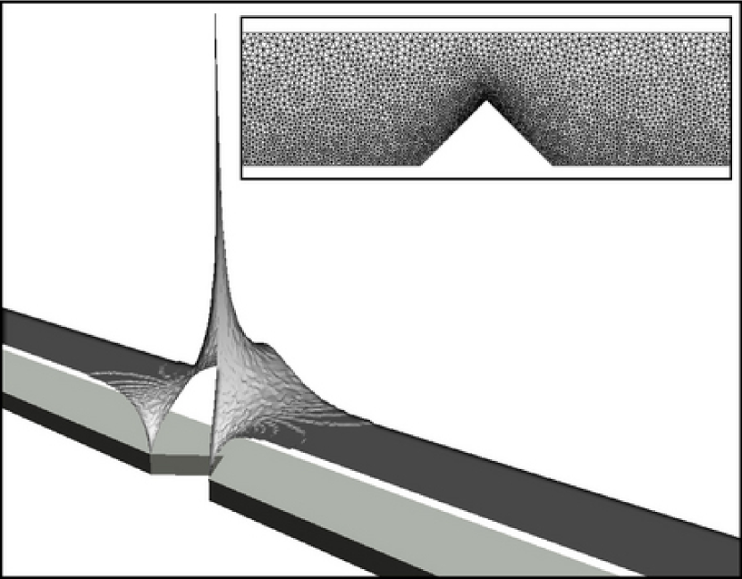
To address this question, the current density distribution can be simulated with finite element modelling according to the method described in the previous section. The model used for the simulation is a 1.2 m long strip (width: 100 nm, thickness: 20 nm) with an indentation in the center. The indentation reduces the width of the strip to 50 nm in the narrowest part. The angle of the indentation is 45∘. The region of interest of the finite element mesh is shown in the inset of Fig. 2. In the vicinity of the notch, the tetrahedral mesh is locally refined to increase the numerical accuracy. A total current of mA is flowing along the wire, and a homogeneous electric conductivity is assumed.
The topographical representation in Fig. 2 displays the local value of the current density. As expected, the current density increases at the constriction. Much more significant than the reduction of the width is, however, the impact of the notch. Where the wire is not constrained, the current density is A/m2. At the apex of the notch, the value increases drastically to A/m2, while in the opposite, flat part of the strip it only increases up to A/m2. Hence, in the narrow part of the strip, the current density distribution is highly inhomogeneous. Over the small distance of 50 nm it changes almost by a factor of four. The values of the local current density obviously scale linearly with the applied current. The value of 2 mA has only been chosen here as an example since the resulting current density values are of the order of those reported in corresponding experimental studies. The current density profile is independent of the value of the applied current. Hence, the inhomogeneities of the current density distribution are directly connected with the sample geometry, and not with the value of the applied current. The profile is moreover invariant with respect to scaling.
The knowledge of this drastically inhomogeneous current density distribution at a notch is expected to be of utmost importance for the design and for the understanding of devices based on current-driven domain-wall displacement. The huge differences of the local current density in the constriction region are expected to have a significant impact on the local strength of the STT effect, the onset of electromigration processes and on the heating of the sample. The seemingly plausible approximation of homogeneous current density distribution in the constriction region hence clearly appears to be inadequate, and should be dropped.
V.2 Oersted field calculation - comparison with analytics
The method presented in section III to calculate the Oersted field for a given current density distribution can be tested by comparing the numerical results with known analytic solutions. A simple example is the magnetic field of an infinitely long current-carrying cylinder with homogeneous current density. The current is flowing parallel to the symmetry axis. If a wire with radius is parallel to the direction, with the current flowing along and and being the azimuthal and radial coordinate, respectively, the Oersted field is
| (26) |
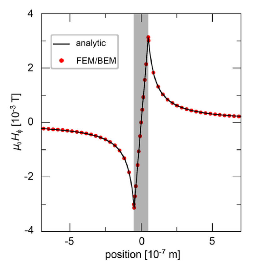
In Fig. 3 this analytical result (solid line) is compared with the computed values (dots) resulting from the FEM/BEM simulation in the case of an 8m long wire with nm and homogeneous current densitiy A/m. Excellent agreement is obtained. Numerical tests show that minor deviations can be further reduced by increasing the discretization density, but are not of practical importance. This example proves the correctness and accuracy of the hybrid FEM/BEM scheme. Obviously, the advantage of the FEM/BEM algorithm is its applicability to samples of complex shape, which cannot be calculated analytically. Such an example is given in the following subsection, where the current density distribution and the resulting Oersted field are calculated for a complex contact geometry as it is used to study current-induced stationary high-frequency excitations of nanomagnets.
V.3 Current densities and Oersted fields in a nanopillar contact geometry
A remarkable difference between the magnetization dynamics induced by spin-polarized electrons as compared to the field induced dynamics is the possibility of generating high-frequency, stationary oscillations in a nanomagnet with a DC current. This effect, which can occur when a sub-micron sized ferromagnetic thin-film element is exposed to a spin-polarized current flowing perpendicularly through its surface, has been predicted Slonc96 ; Berger96 theoretically and confirmed experimentally Kiselev03 . In experimental setups, the thin-film element is usually embedded into a pillar-shaped multilayer nanostructure, which is contacted by mesoscopic leads on the top and on the bottom, so that the electric current flows parallel to the pillar axis. Numerous experimental and numerical studies on the current-induced magnetization dynamics in nanomagnets within a pillar contact have been reported recently (see, e.g., MiltatStiles06 and references therein). While the STT effect is driving the magnetization dynamics, it should be kept in mind that the Oersted field connected with the electric current may represent a non-negligible perturbation which could affect the magnetization dynamics. Considering that also in this case the typical current densities are of the order of A/m2, the Oersted field is expected to provide a sizable contribution even though the pillar dimensions are in the sub-micron range.
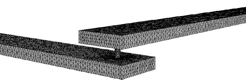
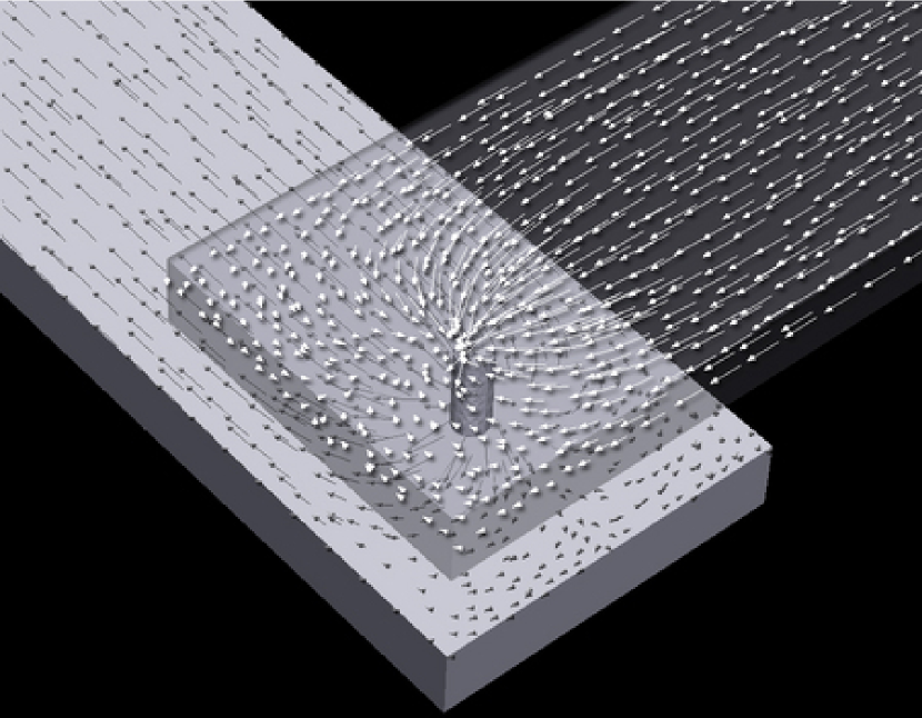
To obtain precise values of the Oersted field in such complicated contact geometries, the approach consists in first simulating the current density distribution in the contact and subsequently calculating the magnetic field. Apart from the current flowing through the pillar, also the current in the leads (which act as what has become known as “strip lines” in the case of field-induced magnetization dynamics) contributes to the total magnetic field acting on the nanomagnet. Fig. 4 shows the finite-element mesh used to simulate the current and field distribution in a pillar contact geometry. In this example, the pillar diameter is 50 nm and the pillar height is 120 nm. It is contacted by strips of 500 nm width and 100 nm thickness. Each contacting strip is 4 m long and the top and bottom electrodes form an angle of 90∘. The geometry roughly corresponds to typical experimental setups Dassow06 , even though the contacting strips are often wider than shown here. The purpose of this simulation is rather to provide an example for the possibility of calculating current density distributions and Oersted fields in realistic geometries than to reproduce all details of a specific experimental setup.
A current of 2 mA is flowing through the sample along the contacting strips. Since the total value of the current and the diameter of the pillar are known, the current density inside the pillar can be trivially calculated without any simulation (yielding A/m2). The same holds for the current density in the contacting strips at regions sufficiently far away from the contact ( A/m2). The more interesting situation occurs in the leads in the vicinity of the contact to the pillar. The complex current density distribution in this region is shown in Fig. 5.
The discretized form of the computed three-dimensional vector field can now be used as an input for the Oersted field calculation. By applying the FEM/BEM algorithm we then obtain the Oersted field in the whole contact geometry. The result is displayed in Fig. 6, where the field circulation around the contacting strips and, in particular, around the pillar can clearly be seen.
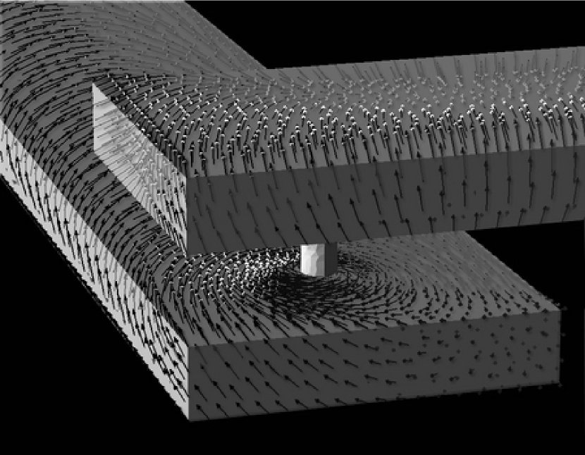
For clarity, only the field in the contacting strips is displayed.
For such experiments and their correct interpretation, the field distribution inside the pillar is decisive. The profile of the field inside the pillar is very similar to the one displayed in Fig. 3: The dominant component of the field is azimuthal, with a magnitude that inside the pillar increases linearly with the distance from the central axis. The peak value at the boundary of the pillar is in this case 28 mT, which certainly represents a non-negligible field. Compared with the field strength due to the current flowing in the pillar, the effect due to the current in the contacting strips can be considered as a perturbation, which provides only an asymmetry along a direction at 45∘ with respect to the strips. Due to this asymmetry, the magnitude of the maximum and the minimum value of both, the and the component of the Oersted field differ by about 12%. Whether the influence of the current through the leads can be neglected depends on the specific experimental setup and the problem that is being investigated. While the field due to the contacting strips may in several cases be safely neglected, it is of essential importance to consider the precise height of the pillar, since it has a direct and decisive impact on the strength of the Oersted field. Reliable calculations of Oersted fields in nanopillar geometries can only be obtained if the height of the current-carrying pillar is known. More details on the influence of the pillar height on the Oersted field and its impact on current-driven magnetization dynamics will be discussed in a forthcoming article.
VI conclusion
The classical interaction of electric currents with the magnetization of ferromagnets is given by the Oersted field. Its importance should not be underestimated in theoretical studies on the emerging field of current-induced dynamic magnetization processes driven by the STT effect. As shown in this study, the values of the Oersted field obtained by using finite-element models of typical experimental contact geometries can be as high as a few tens of mT. In view of these large fields, it appears likely that the details of several current-induced dynamic magnetization processes that are currently studied by many groups are the result of a combination of both, the STT effect and the Oersted field. Thus, for a reliable interpretation of experimental data by means of micromagnetic simulations, the Oersted field may a priori not be neglected. The hybrid FEM/BEM method presented in this article provides a flexible and accurate tool to calculate the Oersted field, and thus to clarify its importance and its influence on the dynamics of nanomagnets in STT studies. The value of the Oersted field depends sensitively on the geometry of the contact setup. For instance, in pillar geometries, the pillar height is of decisive importance.
Also in the case of current-induced domain wall displacement in ferromagnetic strips, some seemingly plausible simplifying assumptions may not be applicable. Micromagnetic simulations should in this case be extended by a routine to calculate the current-density distribution like, e.g., the FEM scheme described in this article. On the example of the frequently used case of indented thin strips, the simulations have shown that geometric variations can have a dramatic impact on the current-density distribution in thin strips. Such a notch can give rise to a strongly inhomogeneous current-density profile along the strip width connected with a strong, localized increase of the current density. It is therefore not sufficient to assume that the increase of current density in such an indented strip simply correlates with the reduction of the cross-section at the notch.
Acknowledgements
I am indebted to Prof. C.M. Schneider for valuable comments on the manuscript and to Sebastian Gliga for precious help on the graphical representation of the computed field and current distributions.
References
- (1) S. I. Kiselev, J. C. Sankey, I. N. Krivorotov, N. C. Emley, R. J. Schoelkopf, R. A. Buhrman, and D. C. Ralph, Microwave oscillations of a nanomagnet driven by a spin-polarized current, Nature 425(6956), 380–383 (2003).
- (2) W. H. Rippard, M. R. Pufall, S. Kaka, S. E. Russek, and T. J. Silva, Direct-Current Induced Dynamics in Co90Fe10/Ni80Fe20 Point Contacts, Phys. Rev. Lett. 92(2), 027201 (2004).
- (3) M. Tsoi, R. E. Fontana, and S. P. P. Parkin, Magnetic domain wall motion triggered by an electric current, Appl. Phys. Lett. 83(13), 26177–26179 (2003).
- (4) N. Vernier, D. A. Allwood, D. Atkinson, M. D. Cooke, and R. P. Cowburn, Domain wall propagation in magnetic nanowires by spin-polarized current injection, Europhys. Lett. 65(4), 526–532 (2004).
- (5) J. C. Slonczewski, Current-driven excitations of magnetic multilayers, J. Magn. Magn. Mater. 159, L1–L7 (1996).
- (6) L. Berger, Emission of spin waves by a magnetic multilayer traversed by a current, Phys. Rev. B 54(13), 9353–9358 (1996).
- (7) Y. Liu, S. Gliga, R. Hertel, and C. M. Schneider, Current-induced magnetic vortex core switching in a Permalloy nanodisk, Appl. Phys. Lett. 91(11), 112501 (2007).
- (8) D. V. Berkov and N. L. Gorn, Micromagnetic simulations of the magnetization precession induced by a spin-polarized current in a point-contact geometry (Invited), J. Appl. Phys. 99(8), 08Q701 (2006).
- (9) E. Martinez, L. Torres, L. Lopez-Diaz, M. Carpentieri, and G. Finocchio, Spin-polarized current-driven switching in permalloy nanostructures, J. Appl. Phys. 97, 10E302 (2005).
- (10) K.-J. Lee, A. Deac, O. Redon, J.-P. Nozières, and B. Dieny, Excitations of incoherent spin-waves due to spin-transfer torque, Nature Mater. 3, 877–881 (2004).
- (11) D. V. Berkov and J. Miltat, Spin-torque driven magnetization dynamics: Micromagnetic Modeling, J. Magn. Magn. Mater. 320, 1238–1259 (2007).
- (12) S. Cherifi, R. Hertel, J. Kirschner, H. Wang, R. Belkhou, A. Locatelli, S. Heun, A. Pavlovska, and E. Bauer, Virgin domain structures in mesoscopic Co patterns: Comparison between simulation and experiment, J. Appl. Phys. 98, 0430901 (2005).
- (13) R. Hertel, O. Fruchart, S. Cherifi, P. Jubert, S. Heun, A. Locatelli, and J. Kirschner, Three-dimensional magnetic-flux-closure patterns in mesoscopic Fe islands, Phys. Rev. B 72, 214409 (2005).
- (14) M. Buess, R. Höllinger, T. Haug, K. Perzlmaier, U. Krey, D. Pescia, M. R. Scheinfein, D. Weiss, and C. H. Back, Fourier transform imaging of spin vortex eigenmodes, Phys. Rev. Lett. 93(7), 077207 (2004).
- (15) J. D. Jackson, Classical Electrodynamics, Wiley, New York, 3rd edition, 1999.
- (16) Y. Acremann, J. P. Strachan, V. Chembrolu, S. D. Andrews, T. Tyliszczak, J. A. Katine, M. J. Carey, B. M. Clemens, H. C. Siegmann, and J. Stöhr, Time-Resolved Imaging of Spin Transfer Switching: Beyond the Macrospin Concept, Phys. Rev. Lett. 96, 217202 (2006).
- (17) K. Ito, T. Devolder, C. Chappert, M. J. Carey, and J. A. Katine, Micromagnetic simulation on effect of oersted field and hard axis field in spin transfer torque switching, J. Phys. D: Appl. Phys. 40, 1261–1267 (2007).
- (18) S. S. P. Parkin, U. S. Patent 6834005 (2004).
- (19) S. Kaka, M. R. Pufall, W. H. Rippard, T. J. Silva, S. E. Russek, and J. A. Katine, Mutual phase-locking of microwave spin torque nano-oscillators, Nature 437, 389–392 (2005).
- (20) Q. Chen, A Review of Finite Element Open Boundary Techniques for Static and Quasi-Static Electromagnetic Field Problems, IEEE Trans. Magn. 33(1), 663–676 (1997).
- (21) S. W. Yuan and H. N. Bertram, Fast adaptive algorithms for micromagnetics, IEEE Trans. Magn. 28, 2031–2036 (1992).
- (22) D. R. Fredkin and T. R. Koehler, Hybrid Method for Computing Demagnetizing Fields, IEEE Trans. Magn. 26(2), 415–417 (1990).
- (23) X. Brunotte, G. Meunier, and J. F. Imhoff, Finite Element Modeling of Unbounded Problems using Transformations: Rigorous, Powerful and Easy Solutions, IEEE Trans. Magn. 28(2), 1663–1666 (1992).
- (24) D. A. Lindholm, Three-Dimensional Magnetostatic Fields from Point-Matched Integral Equations with Linearly Varying Scalar Sources, IEEE Trans. Magn. 20(5), 2025–2032 (1984).
- (25) J. Moussa, L. R. Ram-Mohan, J. Sullivan, T. Zhou, D. R. Hines, and S. A. Solin, Finite-element modeling of extraordinary magnetoresistance in thin film semiconductors with metallic inclusions, Phys. Rev. B 64, 184410 (2001).
- (26) M. Holz, O. Kronenwerth, and D. Grundler, Magnetoresistance of semiconductor-metal hybrid structures: The effects of material parameters and contact resistance, Phys. Rev. B 67, 195312 (2003).
- (27) G. Sarau, S. Gliga, R. Hertel, and C. M. Schneider, Magnetization reversal of micron-scale cobalt structures with a nanoconstriction, IEEE Trans. Magn. 43(6), 2854–2856 (2007).
- (28) H. Dassow, R. Lehndorff, D. E. Bürgler, M. Buchmeier, P. A. Grünberg, C. M. Schneider, and A. D. van der Hart, Normal and inverse current-induced magnetization switching in a single nanopillar, Appl. Phys. Lett. 89(22), 222511 (2006).
- (29) R. D. McMichael and M. J. Donahue, Head to head domain wall structures in thin magnetic strips, IEEE Trans. Magn. 33(5), 4167–4169 (1997).
- (30) M. Hayashi, L. Thomas, C. Rettner, and S. S. P. Parkin, Current-Controlled Magnetic Domain-Wall Nanowire Shift Register, Science 32, 209–211 (2008).
- (31) D. A. Allwood, G. Xiong, M. D. Cooke, C. C. Faulkner, D. Atkinson, N. Vernier, and R. Cowburn, Submicrometer Ferromagnetic NOT Gate and Shift Register, Science 296, 2003–2006 (2002).
- (32) M. Kläui, C. A. F. Vaz, W. Wernsdorfer, E. Bauer, S. Cherifi, S. Heun, A. Locatelli, G. Faini, E. Cambril, L. J. Heyderman, and J. A. C. Bland, Domain wall behaviour at constrictions in ferromagnetic ring structures, Physica B 343(1-4), 343–349 (2004).
- (33) R. Moriya, L. Thomas, M. Hayashi, Y. B. Bazaliy, C. Rettner, and S. S. P. Parkin, Probing vortex-core dynamics using current-induced resonant excitation of a trapped domain wall, Nature Phys. , doi:10.1038/nphys936 (2008).
- (34) J. Miltat and M. D. Stiles, Spin-transfer torque and dynamics, in Spin Dynamics in Confined Magnetic Structures III, edited by B. Hillebrands and A. Thiaville, volume 101 of Topics in Applied Physics, pages 225–308, Springer, 2006.