Corresponding e-mail: ]kj_lee@korea.ac.kr Corresponding e-mail: ]hwl@postech.ac.kr
Current-induced domain wall motion in a nanowire with perpendicular magnetic anisotropy
Abstract
We study theoretically the current-induced magnetic domain wall motion in a metallic nanowire with perpendicular magnetic anisotropy. The anisotropy can reduce the critical current density of the domain wall motion. We explain the reduction mechanism and identify the maximal reduction conditions. This result facilitates both fundamental studies and device applications of the current-induced domain wall motion.
Spin-polarized electrical currents in ferromagnets can transfer their spin angular momentum to local magnetizations via the - exchange interaction and generate torques Berger ; Slonczewski on local magnetizations. This spin transfer torque (STT) received considerable attention in view of both fundamental physics research Grollier ; Klaui1 ; Tatara1 ; Zhang ; Thiaville and applications Parkin ; Allwood .
In a ferromagnetic nanowire, the STT can generate motion of magnetic domain walls (DWs). For conventional metallic ferromagnetic nanowires, which have the in-plane magnetic anisotropy (IMA), experiments Yamaguchi ; Klaui2 ; Hayashi found such current-induced DW motion when the current density in the nanowire is larger than a certain threshold value of the order of A/cm2. This value is too high; At such current densities, the Joule heating generates considerable thermal fluctuations Yamaguchi2 ; Laufenberg ; You , making fundamental studies of the STT difficult. Furthermore device applications Sze require A/cm2 at room temperature. Thus both for fundamental studies and device applications, it is crucial to reduce .
Recently there are experimental Ravelosona and theoretical Fukami indications that may be considerably lower in a metallic nanowire with the perpendicular magnetic anisotropy (PMA). However it remains unclear how the PMA can lower . We aim to answer this question in this Letter.
We consider a nanowire with the wire width along the -axis and thickness along the -axis (). We use the Landau-Lifshitz-Gilbert (LLG) equation with the STT term,
| (1) |
where is the unit vector of the local magnetization, is the gyromagnetic ratio, is the Gilbert damping parameter, is the unit vector of the local current density, and is the effective magnetic field. is the magnitude of the adiabatic STT Tatara1 , where is the electron charge, P is the spin-polarization of the ferromagnet, is the Bohr magneton, and is the saturation magnetization. is the magnitude of the nonadiabatic STT Zhang ; Thiaville with the non-adiabaticity represented by the dimensionless parameter . is independent of and estimated Zhang to be of the order of .
To get an insight into the main physics of the PMA, we first develop an analytical model based on a one-dimensional (1D) approximation. Its results will be later verified by performing the micromagnetic simulations of the LLG equation [Eq. (1)], which are known to provide a reliable description of nanoscale magnetization dynamics Lee ; Seo .
For a ferromagnet with the PMA we have
| (2) |
where is the exchange stiffness constant and is the PMA constant that allows the easy axis (along the -axis) to be perpendicular to the wire-plane (- plane). To describe the demagnetization effects, we consider the magnetostatic dipole-dipole interaction field given by , where the components of the matrix are given by , . Other components of are defined in a similar way.
We also assume that the DW maintains the following shape during the DW motion; , , , where is the equilibrium DW width obtained from 1D micromagnetic simulations. In this rigid DW motion approximation Jung the DW dynamics is described by two dynamical variables, the DW position and the DW tilting angle .
By using the procedure developed by Thiele Thiele , one can then derive, from the LLG equation, the equations of motion for the two collective coordinates and ,
| (3) | ||||
| (4) |
where the pinning force is related to the DW energy per unit cross-sectional area () representing pinning potential in the presence of extrinsic defects in a nanowire. Here is the effective wall anisotropy given by
| (5) |
where () and is the cross-sectional area. represents the magnetostatic energy difference between two types of transverse DWs, the Bloch DW ( at the DW center) and the Neel DW ( at the DW center).
Before we demonstrate its implications for a general case, we first consider a defect-free nanowire () with . in this case is given Tatara1 by
| (6) |
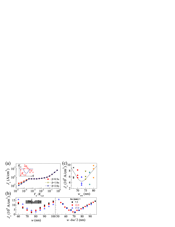
Figure 1(a) shows and dependence of . Note that falls below in a wide range of and . Since all material parameters used in Fig. 1 are similar to those for permalloy except for the PMA constant , this reduction in should be attributed to the PMA. To check the validity of this prediction, we also perform micromagnetic simulations of the LLG equation and excellent agreement is found [Fig. 1(b) upper panel].
This reduction in becomes especially effective when is tuned to a -dependent special value , at which reverses its sign [Fig. 1(b) lower panel] and near , is strongly suppressed. The sign reversal of implies that is the equilibrium phase boundary between the Bloch DW and Neel DW. For transverse DWs in an IMA nanowire, on the other hand, is given by and since is always larger than , in the IMA case is always positive in a conventional nanowire geometry with . This difference between a PMA nanowire and an IMA nanowire illustrates a crucial role played by the PMA.
Next we consider a general case with and . After some calculation, one can obtain an upper bound of Tatara2 ,
| (7) |
where and represents the maximum value of . The dashed line in Fig. 1(c) shows as a function of for a PMA nanowire. For the case , Fig. 1(c) also shows determined from numerical simulations of Eqs. (3) and (4) with the pinning potential energy modelled by a finite ranged harmonic potential [Fig. 1(c) inset]. A few remarks are in order. Firstly, both and exhibit plateaus near in a wide range of . Secondly, depends on only in the weak pinning regime ( Oe) and the dependence essentially disappears in the intermediate (plateau) and strong (above plateau) pinning regimes. This behavior is consistent with the prediction of Eq. (7). Thirdly, a recent experiment Tanigawa with a PMA nanowire finds the depinning magnetic field of about 500 Oe for a field-driven DW motion. When this value is used as an estimation of , one finds A/cm2. Thus Fig. 1(c) demonstrates that the reduction of via the PMA indeed leads to the reduction of . As a comparison, results for an IMA nanowire are also given in Fig. 1(c). Differences from the PMA case are evident.
Next we present micromagnetic simulation results of the LLG equation. Various sources of are examined. Figure 2(a) shows obtained from the 1D LLG equation for a situation where the magnitude of the PMA constant fluctuates from its bulk average value with the maximum deviation given by . Note that the result is remarkably similar to that in Fig. 1(c). In good quality PMA samples, is reported Thomson to be less than 0.1, for which we obtain A/cm2. Figure 2(b) shows the effect of a notch investigated with the two-dimensional (2D) LLG equation. In a wide range of , falls below A/cm2 despite the notch formation. Note that for nm, decreases as the notch depth increases. This strange behavior is not due to the locally enhanced current density near the notch, since this effect should be stronger for nm. Instead it is due to the fact that is determined by an effective wire width that a DW senses. When is plotted as a function of , an estimation of the effective width, this strange behavior disappears and is now almost independent of , in agreement with the prediction in the plateau range in Fig. 1(c). Figure 2(c) shows for a PMA nanowire with the edge roughness and with the PMA fluctuations. Although values of are somewhat scattered with the realizations of the randomness, still remains below A/cm2 in a wide range of the average width Jc-minimum-comment .
Here we remark that all demonstrations for the reduction of assume the proper tuning of and to achieve the reduced . A recent experiment on the PMA nanowire Tanigawa found A/cm2 without such tuning. We suggest that the tuning of and can reduce . Another experiment Ravelosona found indications of the enhanced STT efficiency in a PMA spin valve. However the measurement was still restricted to the thermally assisted creep regime with extremely low DW velocity (average m/s). According to our calculation (not shown), much higher velocity ( m/s) can be achieved at A/cm2 if and are properly tuned. Finally the report Yamanouchi of the reduced in ferromagnetic semiconductors is yet limited to low temperatures ( 100 K) while the reduction scheme presented in this Letter does not require low temperature operation.
In summary, we have clarified the mechanism by which the PMA can drastically reduce . The geometrical tuning is important to maximize the reduction by the PMA. When properly tuned, the dependence of on and the DW pinning force is very weak. This result solves the large thermal fluctuation problem and also makes feasible nanoscale magnetoelectronic devices Parkin ; Allwood based on the current-induced DW motion.
Two authors (SWJ and WK) contributed equally to this work. Critical comments by Sug-Bong Choe, Jae-Hoon Park, and Tae-Suk Kim are appreciated. This work was supported by the KOSEF (SRC Program No. R11-2000-071, Basic Research Program No. R01-2007-000-20281-0, NRL Program No. M10600000198-06J0000-19810), the KRF (No. KRF-2006-311-D00102), and POSTECH (Core Research Program). We acknowledge the support by the KISTI under the Strategic Supercomputing Support Program with Sik Lee as the technical supporter. The use of the computing system at the Supercomputing Center is appreciated.
References
- (1) L. Berger, Phys. Rev. B 54, 9353 (1996).
- (2) J. C. Slonczewski, J. Magn. Magn. Mater. 159, L1 (1996).
- (3) J. Grollier, P. Boulenc, V. Cros, A. Hamzi, A. Vaurs, A. Fert, and G. Faini, Appl. Phys. Lett. 83, 509 (2003).
- (4) M. Klui, C. A. F. Vaz, J. A. C. Bland, W. Wernsdorfer, G. Faini, and E. Cambril, Appl. phys. Lett. 83, 105 (2003).
- (5) G. Tatara and H. Kohno, Phys. Rev. Lett. 93, 086601 (2004).
- (6) S. Zhang and Z. Li, Phys. Rev. Lett. 93, 127204 (2004).
- (7) A. Thiaville, Y. Nakatani, J. Miltat and Y. Suzuki, Europhys. Lett. 69, 990 (2005).
- (8) S. S. P. Parkin, U.S. Patent 6,834,005 (2004).
- (9) D. A. Allwood, G. Xiong, C. C. Faulkner, D. Atkinson, D. Petit, and R. P. Cowburn, Science 309, 1688 (2005).
- (10) A. Yamaguchi, T. Ono, and S. Nasu, K. Miyake, K. Mibu, and T. Shinjo, Phys. Rev. Lett. 92, 077205 (2004).
- (11) M. Klui, C. A. F. Vaz, J. A. C. Bland, W. Wernsdorfer, G. Faini, E. Cambril, L. J. Heyderman, F. Nolting, and U. Rudiger, Phys. Rev. Lett. 94, 106601 (2005).
- (12) M. Hayashi, L. Thomas, C. Rettner, R. Moriya, Y. B. Bazaliy, and S. S. P. Parkin, Phys. Rev. Lett. 98, 037204 (2007).
- (13) A. Yamaguchi, S. Nasu,H. Tanigawa, T. Ono, and K. Miyake, Appl. Phys. Lett. 86, 012511 (2005).
- (14) M. Laufenberg, W. Bhrer, D. Bedau, P.-E. Melchy, M. Klui, L. Vila, G. Faini, C. A. F. Vaz, J. A. C. Bland, and U. Rdiger, Phys. Rev. Lett. 97, 046602 (2006).
- (15) C.-Y. You, I. M. Sung, and B.-K. Joe, Appl. Phys. Lett. 89, 222513 (2006).
- (16) S. M. Sze, VLSI Technology 412 (McGraw-Hill, New York, 1988).
- (17) D. Ravelosona, D. Lacour, J. A. Katine, B. D. Terris, and C. Chappert, Phys. Rev. Lett. 95, 117203 (2005).
- (18) S. Fukami, T. Suzuki, N. Ohshima, K. Nagahara, and N. Ishiwata, Abstr. 52nd Annu. Conf. Magnetism and Magnetic Materials, 2007, FE-06.
- (19) K.-J. Lee, A. Deac, O. Redon, J.-P. Nozires, and B. Dieny Nature Mater. 3, 877 (2004).
- (20) S. M. Seo, W. Kim, T. D. Lee, and K. J. Lee, Appl. Phys. Lett. 90, 252508 (2007).
- (21) S.-W. Jung and H.-W. Lee, J. Magnetics 12, 1 (2007).
- (22) A. A. Thiele, Phys. Rev. Lett. 30, 230 (1973).
- (23) G. Tatara, T. Takayama, H. Kohno, J. Shibata, Y. Nakatani, and H. Fukuyama, J. Phys. Soc. Jpn. 75, 064708 (2006).
- (24) H. Tanigawa, K. Kondou, T. Koyama, K. Nakano, S. Kasai, N. Ohshima, S. Fukami, N. Ishiwata, and T. Ono, Appl. Phys. Express 1, 011301 (2008).
- (25) T. Thomson, G. Hu, and B. D. Terris, Phys. Rev. Lett. 96, 257204 (2006).
- (26) In Figs. 2(b) and (c), is minimized around (or ) near 72 nm, which is somewhat smaller than the value ( nm) in Fig. 1(b). We attribute this difference to the pinning-induced DW deformation.
- (27) M. Yamanouchi, D. Chiba, F. Matsukura, and H. Ohno, Nature (London) 428, 539 (2004).