Electron gas at the interface between two antiferromagnetic insulating manganites
Abstract
We study theoretically the magnetic and electric properties of the interface between two antiferromagnetic and insulating manganites: La0.5Ca0.5MnO3, a strong correlated insulator, and CaMnO3, a band-insulator. We find that a ferromagnetic and metallic electron gas is formed at the interface between the two layers. We confirm the metallic character of the interface by calculating the in-plane conductance. The possibility of increasing the electron gas density by selective doping is also discussed.
pacs:
75.47.Gk, 75.10.-b, 75.30.Kz, 75.50.EeI Introduction

In recent years, atomic control has been gained in the growth of multilayers of thin oxide films with different electronic and magnetic properties. Ohtomo et al. (2002) Interestingly, ’electronic reconstruction’ (or redistribution of charges) at the interfaces of strongly correlated systems Okamoto and Millis (2004a) has led to the appearance of phases showing a very different behavior from that in the bulk of the constituent materials. Ohtomo et al. (2002); Okamoto and Millis (2004a); Ohtomo and Hwang (2004); Okamoto and Millis (2005); Peña et al. (2005); Lee and MacDonald (2006); Brinkman et al. (2007); Reyren et al. (2007); González et al. (2008). For example, superlattices of thin layers of LaTiO3 and SrTiO3 show metallic conductivity, although both materials are insulators in bulk. Ohtomo et al. (2002) SrTiO3 is a band insulator while LaTiO3 is a Mott insulator and has one extra electron on the Ti. This extra charge spreads across the interface producing the metallic behavior. Okamoto and Millis (2004b) Another interesting example is the formation of a high mobility electron gas at the interface between the two band insulators LaAlO3 and SrTiO3. Ohtomo and Hwang (2004) This electron gas has been shown to have magnetic properties Brinkman et al. (2007) and to behave as a two dimensional superconductor at low temperatures. Reyren et al. (2007) The electric field effect, which is the basis for semiconductor transistors, can also be used to tune the charge density at interfaces between strongly correlated oxides, changing their properties. Ahn et al. (2003)
The redistribution of charge in Mott-band insulator heterostructures and the formation of a metallic interface have been studied theoretically using different techniques including Hartree-Fock theory to account for the on-site correlations, Okamoto and Millis (2004a, b) dynamical mean field theory, Okamoto and Millis (2004c) and Lanczos diagonalization of a quasi-one-dimensional lattice. Kancharla and Dagotto (2006) The common observation is the formation of a metallic interface region up to three-unit cells wide. Interfaces between two different Mott insulators have also been theoretically studied: Lee and MacDonald (2006) a two-dimensional metal is formed with a density of states that can be controlled by a remote (a few unit-cells away) doping layer.
Perovskite manganites of formula AA’MnO3 (with the density of electrons) are strongly correlated magnetic materials that present a great variety of phases depending very strongly on the close competition between different interactions: insulating behavior is favored by electron-lattice interaction, Coulomb interaction, and antiferromagnetic superexchange, while ferromagnetism and metallicity are favored by the double-exchange mechanism. Dagotto (2003) By simply changing the doping of a manganite you can go from ferromagnetic and metallic phases to antiferromagnetic and insulating. Phase separation is also commonly observed. Dagotto (2003); Mathur and Littlewood (2003); Israel et al. (2007) All-manganite heterostructures are therefore a very interesting ground for analyzing the interplay between different phases, while minimizing the creation of defects at the interfaces thanks to the similarity in the lattice structure and chemical composition of the layers. Li et al. (2002); Lin et al. (2006); Brey (2007); Niebieskikwiat et al. (2007); Salafranca et al. (2008)
Motivated by the ’electronic reconstruction’ effects observed in different oxide heterostructures and by the range of different phases that manganites show depending on their doping level, we have studied an all-manganite heterostructure formed by two different manganite insulators: La0.5Ca0.5MnO3 (LCMO) and CaMnO3 (CMO). LCMO is a CE-type antiferromagnet (consisting of ferromagnetic zig-zag chains in the x-y plane coupled antiferromagnetically to each other) and insulator in which the antiferromagnetic (AF) superexchange and the Jahn-Teller interaction open a gap in the band structure. On the other hand, CMO is a parent compound with no electrons on the Mn sites and, therefore, a band insulator. CMO presents AF () ordering (G-type) due to the superexchange between the electrons.
By looking at the band structure and the in-plane conductance of these heterostructures, we find that a ferromagnetic (FM) and conducting interface can be formed for a range of reasonable parameters. We also find that by changing the electron concentration in LCMO around half-doping, , the charge in the metallic interface and the in-plane conductance can be manipulated.
II Model
We study the heterostructure depicted in Fig. 1 consisting of alternating CMO and LCMO layers a few unit cells wide. The background charge (namely, the charge on the AO planes) is in the CMO planes, in the LCMO planes and, to achieve a symmetric distribution of the charge, we use the average at the interfaces. To study the phase diagram, different magnetic configurations on the CMO planes (either FM or G-type AF) are considered. On the other hand, the magnetic order in the LCMO planes is always considered to be of the CE-type: FM zig-zag chains in the x-y plane coupled antiferromagnetically with neighboring chains. As discussed below, FM planes in the LCMO layer are not favored energetically.
The hamiltonian Brey (2004, 2007); Salafranca et al. (2008) includes the kinetic energy, a nearest neighbor antiferromagnetic coupling, and a Hartree term that takes into account the long range Coulomb interaction between all the charges in the system
| (1) |
where creates an electron on the Mn i-site, in the orbital ( with and ). The hopping amplitude depends on the Mn core spins orientation given by the angles and via the double-exchange mechanism
| (2) |
and on the orbitals involved where the superindices x,y, and z refer to the direction in the lattice. All the parameters are given in units of which is estimated to be eV. is, in general, an effective antiferromagnetic coupling between first neighbor Mn core spins which is different in the CMO and LCMO layers. For CMO, the antiferromagnetic coupling is a pure superexchange between the localized t2g spins, while for LCMO it would effectively include the interaction between the eg electrons and the lattice. van den Brink et al. (1999) takes the form
| (3) |
with the position of the Mn ions, the occupation number on the Mn i-site, the charge of the A-cation located at , and the dielectric constant of the material. The relative strength of the Coulomb interaction is given by the parameter [Lin et al., 2006].
We are assuming that the eg Mn levels in the two different layers are aligned, although a band offset due to a mismatch in the work functions of the two materials could occur. Lee and MacDonald (2006) We expect our approximation to be reasonable as the two layers are chemically similar.
We find the ground state configuration (at temperature ) of the heterostructure by solving the hamiltonian in Eq. 1 self-consistently in a system ( unit cells of CMO and other of LCMO, as depicted in Fig. 1) with periodic boundary conditions in the three directions. Bulk behavior is always recovered at the center of the layers and the two CMO/LCMO interfaces (at planes and planes ) are independent of each other.
III Results
III.1 Phase diagram


In Fig. 3 we show the phase diagram of the heterostructure built by comparing the energies of four different configurations in the CMO layer. All the considered configurations have a symmetry plane between planes and in Fig. 1: (i) the configuration labeled FM corresponds to G-type AF order on all CMO planes ( to , and to ); (ii) FM stands for one FM plane at each interface ( and ); (iii) FM stands for two FM planes at each interface ( and on one interface, and and on the other); and, finally, (iv) FM corresponds to all FM CMO. We have checked that having FM planes in the CMO layer is more favorable energetically than having FM planes in the LCMO layer. This is mainly due to the fact that the Jahn-Teller coupling occurring in bulk LCMO, and absent in bulk CMO (with no eg electrons), implies a larger effective AF superexchange in the former, van den Brink et al. (1999) making AF order more robust in LCMO than in CMO.
As the LCMO layer has a fixed CE configuration in all planes, the phase diagram is independent of the coupling and it only depends on which is a pure AF superexchange ( meV [Dagotto, 2003]). An estimation of in units of the hopping parameter eV would be . In Fig. 3 we plot the phase diagram as a function of and . A likely value for is in the range [Lin et al., 2006].
In Fig. 3 we show the electronic density per plane and the Hartree potential for the FM, FM, and FM configurations. The results are shown for (the curves are qualitatively similar for different values of ). Fig. 3 illustrates the charge spreading across the interface and how it is limited by the Coulomb interaction between all the charges in the system, given by the average on each plane of the Hartree potential, which at site takes the form
| (4) |
The bulk values for the electronic density are recovered in the center of both CMO and LCMO layers. The curves for the FM (not shown) are almost coincident to the ones corresponding to FM.
The phase diagram (Fig. 3) shows that configurations with ferromagnetic planes are the ground state for the lowest values of the . For reasonable values of this parameter, the ground state is the FM configuration. From now on, we focus on this particular case.
III.2 Analysis of the metallic interface: density of states, conductance, and ’shadow’ order.
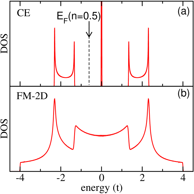

We analyze now the properties of the ground state FM configuration by looking at the density of states (DOS), the in-plane conductance, and the charge distribution on each of the planes. As a reference, let us first discuss the density of states of a 2-dimensional CE system illustrated in Fig. 5 (a). For the first band is completely full and the system is an insulator. For , the extra electrons would have to go to the non-dispersive band at energy, but this requires a large energy, of the order of the gap, so the system would probably tend to phase separate with FM regions (this is the case of PrnCa1-nMnO3 [Jirak et al., 1985]). This phase separated system would also be insulating. For , assuming the CE order is not altered, the first band would be partially full, there would be a finite DOS at the Fermi energy, and the system would be conducting. However, the experimental observation is somewhat different: for it is possible that an incommensurate charge-orbital order arises opening a gap at the Fermi energy, Milward et al. (2005); Brey and Littlewood (2005) leading to insulating behavior. The DOS of a 2-dimensional FM with two eg orbitals has the peculiar shape shown in Fig. 5 (b).
In Fig. 5 we show the DOS on planes to of the CMO/LCMO heterostructure in the FM configuration. The Fermi energy (EF) is signaled by the dashed vertical line crossing the six panels. The shape of the DOS of a perfect CE (as in Fig. 5 (a)) is recovered in planes and , except for an overall shift due to the Hartree potential [Fig. 3 (b)]. The electronic density in plane is exactly (see Fig. 3), the EF is at the gap, and the plane is an insulator. On the other hand, the electronic density in plane is slightly smaller than , there is a finite DOS at EF and, therefore, this CE plane conducts. The CE plane adjacent to the FM plane () has a DOS very different from that of a perfect CE, in particular, the gap at the EF closes and the plane conducts. The FM plane () shows no gaps, as expected. We have also performed numerical calculations via the Kubo formula Vergés (1999); Calderón et al. (1999) of the in-plane conductance that quantify these observations. In particular, by connecting the planes one by one to the leads, we have calculated each plane’s conductance. The results are shown in Fig. 6 (a) and show that three planes (, , and ) conduct. However, following the discussion in the previous paragraph, it is clear that the finite conductance we find in the CE planes is an artifice of our approximation of having fixed the CE magnetic ordering on the LCMO planes: it is possible (and consistent with experimental observations) that other complicate magnetic and charge-orbital orders or phase separation arose, leading to an insulating behavior. Exploring these other possibilities is out of our computing capabilities and we expect that imposing an insulating character on the doped CE phases would not affect the electrostatics of the system. The most reasonable interpretation of our results is illustrated in Fig. 6 (b) where only the finite conductance in the FM plane is kept.
Another important observation is that the DOS of the FM plane at the interface () is very different from that of an isolated 2-dimensional ferromagnet [see Fig. 5 (b)]. This is a manifestation of the influence produced by the adjacent G and CE planes. This strong influence is also revealed by the appearance of a charge modulation (’shadow’ order) on the FM plane in the heterostructure, illustrated in Fig. 7. Here we show both the magnetic ordering (G, FM, and CE) and a qualitative representation of the charge and orbital configurations for planes , , , and . Black dots correspond to sites with more charge than in gray dots. The elongated dots represent orbital order. The charge modulation, which is absent in plane , arises in planes and due to the fact that some sites have neighbors with a parallel spin in the z-direction while others have antiparallel neighbors. Double exchange mechanism implies that hopping is not allowed in the case of antiparallel spin and, consequently, the charge is larger at those sites with more parallel neighbors.


III.3 Selective doping on the LCMO layer
We now explore the effect of doping the LCMO layer to produce a small increase or decrease of electronic density (electron or hole doping, respectively). The considered heterostructure is still the same as in Fig. 1 but now the charge on the center slab is [ at the interfaces]. The phase diagrams for the cases are very similar to the one for shown in Fig. 3. However, due to the asymmetry Milward et al. (2005); Brey and Littlewood (2005) on the electron or hole doping around , manifest on the shape of the DOS in Fig. 5 (a), we expect, and indeed observe, a qualitatively different behavior for and in terms of the charge distribution.
In Fig. 8 we show the electron density and Hartree potential for , and . For , the electrons on excess of cannot be accommodated in the center of the LCMO layer due to the gap in the DOS [Fig. 5] so they go to the LCMO planes close to the interface and to the FM plane. On the contrary, the defect of electrons for the case easily accommodates at the center of the LCMO layer and there is an overall decrease of the electron density at all planes. Consequently, the electron density in the FM plane increases with increasing .
The in-plane conductance in the FM plane as a function of around half-doping is shown in Fig. 9 for . For this particular value of , the conductance increases with both electron and hole doping around . However, the shape of the curve is different for different values of . This variability is due to the complicated structure (with many maxima and minima) of the DOS in the FM plane (see Fig. 5). The structure on the DOS arises from the interplay between the DOS of a perfect CE [Fig. 5 (a)], that of 2-dimensional FM [Fig. 5 (b)], and that of a G plane (single peak at energy), shifted relatively to each other by the Hartree potential. Changing and/or produce a change in both the Fermi energy and the Hartree potential so the peaks on the DOS move with respect to each other. As the conductance is a measure of the DOS at EF, it is not surprising that small changes in and can produce relatively large changes in .

IV Conclusions
The possibility of growing good quality oxide heterostructures is opening a new playground to study both fundamental aspects of strongly correlated systems and the competition between their different phases, and potential applications of the new phases that arise at the interfaces. Manganites, with their very rich phase diagrams, are excellent candidates to analyze all these issues.
Here we have studied an all-manganite heterostructure consisting of a band insulator (CaMnO3) and a half-filled ordered manganite (La0.5Ca0.5MnO3) in which the insulating behavior is driven by strong correlations in the system. We use a model which has been proved successful in reproducing the phase diagram of bulk manganites. van den Brink et al. (1999) The Coulomb interaction between the charges in the system, introduced at a Hartree level, produces a spreading of the charge across the interface. This leads to the formation of a metallic and ferromagnetic plane at the interface, similarly to what has been observed in heterostructures of Mott and band insulators, Okamoto and Millis (2004a) for a wide range of physical parameters. We have characterized this interface by its density of states and the in-plane conductance. The ferromagnetic metal at the interface shows charge and orbital modulation due to the interaction with the ordered neighboring planes. Finally, we have also observed that small electron and hole doping in the La0.5Ca0.5MnO3 layer can produce large changes in the conductance of the ferromagnetic metallic interface.
This work is supported by MAT2006-03741 (MEC, Spain). J.S. also acknowledges FPU program (MEC, Spain) and M.J.C. Ramón y Cajal program (MEC, Spain).
References
- Ohtomo et al. (2002) A. Ohtomo, D. Muller, J. Grazul, and H. Hwang, Nature 419, 378 (2002).
- Okamoto and Millis (2004a) S. Okamoto and A. Millis, Nature 428, 630 (2004a).
- Ohtomo and Hwang (2004) A. Ohtomo and H. Y. Hwang, Nature 427, 423 (2004).
- Okamoto and Millis (2005) S. Okamoto and A. Millis, Phys. Rev. B 72, 235108 (2005).
- Peña et al. (2005) V. Peña, Z. Sefrioui, D. Arias, C. Leon, J. Santamaria, J. L. Martinez, S. G. E. te Velthuis, and A. Hoffmann, Phys. Rev. Lett. 94, 057002 (2005).
- Lee and MacDonald (2006) W.-C. Lee and A. H. MacDonald, Phys. Rev. B 74, 075106 (2006).
- Brinkman et al. (2007) A. Brinkman, M. Huijben, M. van Zalk, J. Huijben, U. Zeitler, J. C. Maan, W. G. van der Wiel, G. Rijnders, D. H. A. Blank, and H. Hilgenkamp, Nature Materials 6, 493 (2007).
- Reyren et al. (2007) N. Reyren, S. Thiel, A. D. Caviglia, L. F. Kourkoutis, G. Hammerl, C. Richter, C. W. Schneider, T. Kopp, A.-S. R etschi, D. Jaccard, et al., Science 317, 1196 (2007).
- González et al. (2008) I. González, S. Okamoto, S. Yunoki, A. Moreo, and E. Dagotto (2008), arXiv:0801.2174.
- Okamoto and Millis (2004b) S. Okamoto and A. Millis, Phys. Rev. B 70, 075101 (2004b).
- Ahn et al. (2003) C. H. Ahn, J. M. Triscone, and J. Mannhart, Nature 424, 1015 (2003).
- Okamoto and Millis (2004c) S. Okamoto and A. Millis, Phys. Rev. B 70, 241104(R) (2004c).
- Kancharla and Dagotto (2006) S. S. Kancharla and E. Dagotto, Phys. Rev. B 74, 195427 (2006).
- Dagotto (2003) E. Dagotto, Nanoscale Phase Separation and Colossal Magnetoresistance (Springer-Verlag, Berlin, 2003).
- Mathur and Littlewood (2003) N. D. Mathur and P. B. Littlewood, Physics Today 56, 25 (2003).
- Israel et al. (2007) C. Israel, M. J. Calderón, and N. D. Mathur, Materials Today 10, 24 (2007).
- Li et al. (2002) H. Li, J. R. Sun, and H. K. Wong, Appl. Phys. Lett. 80, 628 (2002).
- Lin et al. (2006) C. Lin, S. Okamoto, and A. J. Millis, Phys. Rev. B 73, 041104 (2006).
- Brey (2007) L. Brey, Phys. Rev. B 75, 104423 (2007).
- Niebieskikwiat et al. (2007) D. Niebieskikwiat, M. B. Salomon, L. E. Hueso, N. D. Mathur, and J. A. Borchers, Phys. Rev. Lett. 99, 247207 (2007).
- Salafranca et al. (2008) J. Salafranca, M. J. Calderón, and L. Brey, Phys. Rev. B 77, 014441 (2008).
- Brey (2004) L. Brey, Phys. Rev. Lett. 92, 127202 (2004).
- van den Brink et al. (1999) J. van den Brink, G. Khaliullin, and D. Khomskii, Phys. Rev. Lett. 83, 5118 (1999).
- Jirak et al. (1985) Z. Jirak, S. Krupicka, Z. Simsa, M. Dlouham, and S. Vratislav, J. Magn. Magnetic Mater. 53, 153 (1985).
- Milward et al. (2005) G. Milward, M. J. Calderón, and P. B. Littlewood, Nature (London) 433, 607 (2005).
- Brey and Littlewood (2005) L. Brey and P. B. Littlewood, Phys. Rev. Lett. 95, 117205 (2005).
- Vergés (1999) J. Vergés, Comp. Phys. Comm. 118, 71 (1999).
- Calderón et al. (1999) M. J. Calderón, J. A. Vergés, and L. Brey, Phys. Rev. B 59, 4170 (1999).