A triple quantum dot in a single wall carbon nanotube
Abstract
A top-gated single wall carbon nanotube is used to define three coupled quantum dots in series between two electrodes. The additional electron number on each quantum dot is controlled by top-gate voltages allowing for current measurements of single, double and triple quantum dot stability diagrams. Simulations using a capacitor model including tunnel coupling between neighboring dots captures the observed behavior with good agreement. Furthermore, anti-crossings between indirectly coupled levels and higher order cotunneling are discussed.
Carbon nanotubes (CNTs), a promising material for quantum information devicesSapmaz2006NanoLett ; Loss1998PhRvA , are one-dimensional systems with remarkable coherency of electrons. It is therefore attractive to electrostatically define quantum dots, also known as artificial atoms, along the length of the CNT. Electron transport through a two-atomic moleculevanderWiel consisting of two coupled quantum dots in a CNTBiercuk2003NanoLett ; Mason2004Sci ; Biercuk2005NanoLett ; Sapmaz2006NanoLett ; Graeber2006PhRvB ; Graeber2006SeScT ; Jorgensen2006ApPhL probes molecular states in which the electron is delocalized over the two quantum dots. Scaling the system further up to three coupled quantum dotsWegewijsPRB ; WegewijsJJAP2001 or a tri-atomic artificial molecule enables the study of more intriguing phenomena related to electrostaticsWaugh1995PhRvL ; Waugh1996PhRvB ; SchroerPRB and molecular states of the triple quantum dot (quantum superposition of three levels). Coupled three level systems might allow for future experiments inspired by the field of quantum opticsBrandesReview ; Renzioni2001Adiabatictransfer ; Greentree2004PhRvB ; BenakkerEurophys ; Emary2007 and are also attractive from a quantum information point of viewMeierqbitcluster ; Zhang2004entangler . In contrast to GaAs defined triple quantum dots, which can be (or sometimes unintentionally are) arranged in a triangular configurationGaudreau2006PhRvL ; Korkusinski2007 ; Ihn ; StopaPRL2002Rectifying ; VidanAPL2004 ; SagaraTriangularEntangle ; Emary2007 , the CNT geometry ensures the serial and simplest configuration, where electrons only tunnel between neighboring dots. Furthermore, the more challenging experiments of investigating the serial triple quantum dot Kondo effectZitko2006PhRvB are yet to be addressed experimentally.
In this Letter we present measurement on a top-gated single wall carbon nanotube showing individual control of three coupled quantum dots defined between the source and drain electrodes. The characteristics are understood as transport through molecular states rather than sequential tunneling through three dots. Charging effects with different capacitive and tunnel couplings between neighboring quantum dots are investigated by an electrostatic capacitor model including first order tunneling processes. Finally, a discussion of triple quantum dot characteristics as second order anti-crossings and higher order cotunneling is presented.
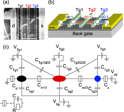
The devices are fabricated by an initial step to define Pt/Ti (40 nm/5 nm) alignment marks on top of a SiO2 capped (500 nm) highly doped Si substrate. Subsequently, catalyst islands of Iron-nitrate (Fe(NO3), Molybdenum acetate (MoO2(CH3COO)2) and Al-oxide nano-sized particles in methanol are deposited relative to the alignment marks. Single wall carbon nanotubes are grown from the catalyst islands by chemical vapor deposition at 850-950 ∘C in a mixture of methane, argon and hydrogen. Electrodes (Au/Ti) are defined some microns away from the catalyst islands in hope that one nanotube bridges the electrode gapJorgensen2006ApPhL . Top-gate electrodes (8 nm Al oxide followed by 10 nm Al and 25 nm Ti) are defined on top of the nanotube and a final optical lithography step is used to make the bonding pads. A scanning electron micrograph of a similar device with a nanotube crossing the gap between the two electrodes is shown in Fig. 1(a).
Figure 1(b) schematically shows the cross-section of the device. Three top-gates are defined (Tg1-3) between the source and drain electrodes contacting the nanotube. The tunnel rate between the drain/source electrode and the nanotube is , which to some extent is determined by the choice of electrode materialJavey2003Sm ; KimAPL2003 ; Babic . The choice of Ti for this device yields tunnel barriers high enough to obtain single electron tunneling characteristics (see below).
In case of a semiconducting CNT, the backgate can adjust the electrochemical potential of the CNT into the valence/conduction band while the top-gates can introduce barriers below the gates by locally tuning the electrochemical potential into the band gap. By inducing tunnel barriers under selected top-gate electrodes, several quantum dot structures can be imagined as e.g. a (tunable) single, double, triple or even quadruple quantum dot. However, sometimes barriers are formed at zero gate voltage probably due to defects introduced during the electron beam lithography or evaporation process. In this particular device, tunnel barriers are formed under the two outermost top-gates (Tg1 and Tg3), but not under the central top-gate (Tg2) as evidenced from the following measurements. Each top-gate controls the electrostatic potential of (some of) the dots, QD1, QD2 and QD3, while the tunnel barriers are less affected. The obtained triple quantum dot is illustrated in Fig. 1(b) with the different colored ovals showing the position of the three quantum dots (black, red and blue). The electrostatic behavior is captured in Fig. 1(c), where the device is represented by a capacitance model with tunnel coupling between neighboring dots. Negligible direct capacitive coupling between QD1 and QD3 is expected for the serial geometry. Furthermore, cross capacitances are inserted as deduced from measurements below and capacitive coupling to the backgate is included.
In the sequential tunneling regime with very high barriers, transport through the triple quantum dot is only allowed at certain quadruple points in the three dimensional gate space spanned by , and , where four charge states are degenerateSchroerPRB . However, we observe large cotunneling current in a wide region of gate space, which can be interpreted as transport through molecular states of the triple quantum dot. The interdot tunnel couplings ( and ) formed under the top-gates are strong enough to form a coherent superposition (molecular state) over the triple dot, which is weakly coupled to the Ti source/drain electrodes.
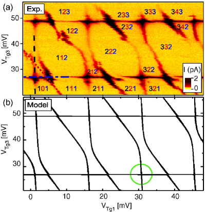
Figure 2(a) shows the current through the triple quantum dot versus Tg1 and Tg3 with constant voltage on Tg2 at finite bias voltage having (overall) vertical, sloping and horizontal lines. Examples are shown by black (dashed), red (dotted) and blue (dash-dotted) lines in the lower left of the figure111Several gate switches were observed during measurements despite keeping the gate ranges very small. Figure 2 has therefore been translated along the gate axes -6.5 mV and V to correct such switches relative to Fig. 3.. The vertical, sloping and horizontal lines correspond to adding an electron to QD1, QD2 and QD3, respectively. It is seen that sweeping only Tg1 adds electrons to QD1 (crossing vertical lines) and QD2 (crossing sloping lines), while sweeping only Tg3 adds electron to QD2 (crossing sloping lines) and QD3 (crossing horizontal lines). Tg1/3 therefore couples capacitively to both QD1/3 and QD2 as schematically drawn in Fig. 1(c). The charge states are shown in the plot, where is the additional electron number in QD , . The observed behavior can, however, not solely be explained by electrostatics (without coupling). A relative large tunnel and capacitive coupling is seen at (anti)crossings between sloping and vertical lines in contrast to the crossings between sloping and horizontal lines. Thus the capacitive () and tunnel coupling () between QD1 and QD2 are relatively large compared to the capacitive and tunnel coupling between QD2 and QD3 (DQD23). Furthermore, the direct capacitive coupling between QD1 and QD3 is as expected small because a crossing behavior is observed between horizontal and vertical lines. Since an electron can not tunnel from QD1 to QD3, no direct tunnel coupling between QD1 and QD3 exists in contrast to the triangular triple quantum dot geometry. This crossing will be subject for further discussion below.
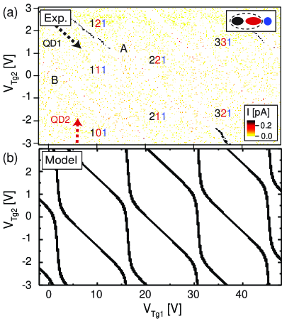
We can also probe a more familiar charging effect on a double quantum dot formed by QD1 and QD2 (DQD12). Figure 3(a) shows the current through the triple quantum dot versus Tg1 and Tg2 at finite bias voltage. The voltage on Tg3 is fixed leaving QD3 in Coulomb blockade with a constant number of electrons. A (tilted) honeycomb pattern is revealed as expected for a double quantum dot with finite current primarily along sloping and vertical lines due to electrostatics. Crossing the vertical lines correspond to adding an electron to QD1, while crossing the sloping lines similarly correspond to adding an electron to QD2. When increasing Tg1 for constant Tg2 both vertical and sloping lines are crossed indicating a capacitive coupling from Tg1 to both QD1 and QD2, respectively, as deduced above as well (Fig. 2). In contrast only sloping lines are crossed when increasing Tg2 for constant Tg1 illustrating that there is no cross capacitance from Tg2 to QD1 (thus part of the deduced schematics in Fig. 1(c)). Consistent with Fig. 2(a), the strong anti-crossings observed between sloping and horizontal lines reveals the presence of a significant electrostatic () and tunnel coupling () between QD1 and QD2. This indicates that transport involves molecular ground states, e.g., the transport around A (lower wing) is due to a degeneracy between the 111 charge state and the ground state of the quantum superposition involving the 121 and 211 charge states. Some variation in the tunnel and capacitive coupling is observed, e.g., stronger coupling between the 211 and the 121 states (anti-crossing at A) than between the 101 and 011 states (anti-crossing at B).
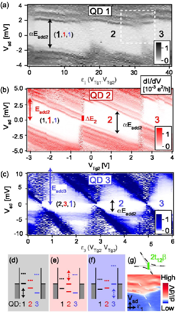
We can also investigate each single QD by sweeping the top-gate voltages, for example along the black or red dashed arrows in Fig. 3(a) for the measurement of QD1 and QD2, respectively. Similarly, QD3 can be probed as well (not shown)222Condition for top-gate voltages Tg1-3, QD1: mV mV, V V (), mV (); QD2: mV (), mV (); QD3: mV (), V V (), mV mV.. Figure 4(b) shows the stability diagram of QD2 by adjusting the electrochemical potentials of QD2 only (see Fig. 4(e)) via Tg2. It reveals clear Coulomb blockade diamonds due to addition of electrons in QD2 with an addition energy of meV and excited states with a level spacing of meV (see arrow and vertical bar, respectively). Similarly, the stability diagram of QD3 in Fig. 4(c) shows well defined Coulomb blockade diamonds with an estimated addition energy of meV (blue arrow) and a less clear level spacing around meV. However, additional horizontal lines are visible at low finite bias attributed to transport through molecular states primarily related to the electron being localized in QD2 (i.e. source or drain chemical potentials being aligned with (red) electrochemical potentials of QD2 in Fig. 4(f)). The bias gap between the highest negative and lowest positive lines therefore corresponds to the addition energy of QD2 scaled by a capacitance dependent factor indicated by the black arrow in Fig. 4(a-c). Finally, the stability diagram of QD1 is shown in Fig. 4(a) exhibiting a less regular behavior. The Coulomb diamonds are cut off at finite bias due to tunneling through molecular states as the case of QD3, which makes it more difficult to estimate the addition energy. An estimate of diamond (2,1,1) yields meV. Also in this case the scaled addition energy of QD2 matches the bias gap (black arrow) between lowest finite bias lines, and the fine structure at higher bias is in agreement with the level spacing of QD2. The bias voltage position of the finite bias lines in QD1 (Fig. 4(a)) are shifted by changing voltage on Tg2, i.e., tuning the electrochemical potential (molecular states) of QD2 consistent with the above interpretation (not shown).
It should be noted that the transport characteristics is different from weakly coupled triple quantum dots in the sequential tunneling regime. Transport is allowed even when only one of the QD is located in the transport window while others are in the Coulomb blockade regime. We observe larger current when two QDs are in the transport window as seen at the crossing points of conductance lines in Fig. 2, and even larger current at the quadruple point (not shown). A more thorough discussion of the current in terms of cotunneling follows below. We also note that the observed characteristic of relatively strong interdot tunnel coupling is incompatible with transport through three parallel CNTs, since they only would be capacitively coupled. The molecular state interpretation of the triple dot measurements is further supported by the following calculation based on the capacitance model shown in Fig. 1(c). We try to estimate a reasonable set of parameters (12 capacitances and two tunnel couplings) by calculating stability diagrams of the capacitor circuit shown in Fig. 1(c) including single electron tunneling processes within the triple quantum dot. The general features of the resulting stability diagram (the vertical, sloping and horizontal lines) are due to electrostatics, which are primarily determined by the top-gate capacitances vanderWiel ; SchroerPRB (see Supporting Information S1). The deduced charging energies , and from the single quantum dot measurements in Fig. 4(a-c) depend on the total capacitance of each dot and are related to the capacitances of the model by ()SchroerPRB
| (1) | |||||
| (2) | |||||
| (3) |
where , is the sum of the capacitances directly connected to QD , i.e., , and (see Supporting Information S1). The charging energies obtained and used in the model are meV, meV and meV. As pointed out in the analysis of the measurements, the coupling between QD1 and QD2 is stronger than the coupling between QD2 and QD3 yielding coupling energies meV meV (see Supporting Information). Geometrical considerations on the device structure are also used to estimate the backgate capacitances333The length between the contacts and the lengths of QD1-3 are m and , with m fixed (assuming the CNT crosses perpendicular to the contacts). The top-gates are made in a second electron beam lithography step aligning to predefined markers and we here assume a 100 nm shift (often observed) to the right relative to the contacts making QD3 small consistent with measurements (high charging energy ). The estimated lengths of QD1 and QD2 therefore become m and m yielding backgate capacitances according to , where for Si-oxide with height nm and nm is the diameter of the CNTMcEuen . and the 12 capacitances are listed in Table 1.
Given all the capacitances in the model, electrostatic stability diagrams can be calculatedSchroerPRB by finding the charge (ground) state having the lowest electrostatic energy . When the tunnel couplings are included, the charge states with the same total number of electrons on the triple quantum dot couples together forming molecular states (e.g. , (1,0,0), (0,1,0) and (0,0,1) couple together). The eigenenergies for a total electron number on the triple quantum dot is found by diagonalising the corresponding matrix with the diagonal elements given by the electrostatic energies and the off-diagonal elements being zero except when two charge states are connected by one tunneling event, e.g., (1,0,0) is connected with (0,1,0) by and (0,1,0) is connected with (0,0,1) by . When the molecular ground state energy with a total number of electrons on the triple quantum dot is equal to the ground state energy with electrons, transport is allowed. The model therefore describes the measurement by ground state transport through molecular triple quantum dot states. More details are given in the Supporting Information S2.
| [aF] | [aF] | [aF] | [aF] | ||||
|---|---|---|---|---|---|---|---|
| Tg1 | 11 | bg1 | 8.6 | Tg1QD2 | 9.5 | cm12 | 2 |
| Tg2 | 0.05 | bg2 | 28.5 | Tg3QD2 | 6 | cm23 | 0.2 |
| Tg3 | 7.3 | bg3 | 2.9 | s | 2.9 | d | 5 |
Figure 2(b) shows the resulting plot, which resembles the main features of the measurement in Fig. 2(a) with good agreement444The origin (0,0,0) of in the model is translated to (-5.5 mV,0 V,16 mV) to match the experimental voltages exactly in Fig. 2 and 3. Furthermore, the model calculation in Fig. 3 has been shifted by the addition of one electron in QD2, i.e., V, since the model triple quantum dot is empty for negative voltages on .. The electrostatic part of the model captures the charging effects, while the tunnel part (and capacitive interdot coupling) makes strong/weak anti-crossing behavior for DQD12/DQD23. We obtain tunnel couplings meV and meV from the analysis, where the tunnel coupling is an upper bound. An estimate of the anti-crossing between levels in QD1 and QD2 () can also be found from the bias stability diagram of QD1 shown in Fig. 4(a), e.g., in the dashed box shown in another color scheme in Fig. 4(g). The lower white dashed line in Fig. 4(g) follows the edge of the Coulomb diamond (mainly a level in QD1), which makes an anti-crossing with a horizontal line (mainly a level in QD2) as the bias is increased. See also Fig. 4(a), where no dashed guide lines are drawn. The schematic of this behavior is shown in the top panel of Fig. 4(g) with the strength of the anti-crossing being pure tunnel-like (i.e. no interdot capacitance). An estimate along the bias direction (green bar) yields meV in agreement with the average value obtained from the model. The capacitance dependent factor is in this case close to 1, since the electrochemical potentials in QD1 are only little affected by changing the voltage on the source. A more complicated anti-crossing behavior involving excited states is also observed at higher bias voltage. Finally, the model also describes the measurements when sweeping another set of top-gates as e.g. shown in Fig. 3(a-b) for DQD12. Since Tg1 and Tg2 do not couple to QD3, a well coupled double quantum dot honeycomb structure is observed consistent with the triple quantum dot stability diagram. A double quantum dot DQD23 is also formed between QD2 and QD3, which shows very weak anti-crossings as expected (not shown) from the above measurement.
The model presented here is the simplest approach to a coupled triple quantum dot ignoring shell structure, spin and the effect of hybridization to the leads. The shell structure is to some extent visible in the measurement, since the addition energies are not constant throughout the gate sweeps shown. This is supported by the single QD stability diagrams, where excited states are observed (Fig. 4). However, the shell structure is unfortunately not clear enough to assign even/odd or four-fold electron occupation for the filling. These effects are therefore not included in the model in the simplest approach. In case of clear shell structure, an interesting topic would be to study exchange interaction in the triple quantum dot system. The model assumes constant (average) tunnel and capacitive couplings even though the coupling between the different charge states (orbitals) vary in the measurements as mentioned.
We will end by briefly discussing two phenomena in triple quantum dots based on the above model and experiment. We focus on a gate voltage-region, where a vertical and a horizontal line cross as e.g. marked by the green circle in the model calculation of Fig. 2(b) and magnified in Fig. 5(a) (black lines). The electrochemical potential of QD1 and QD3 at the crossing are aligned with the chemical potential of the leads, while QD2 is in Coulomb blockade as shown in Fig. 5(c). The current profile along the vertical resonance line indicated by the blue arrow in Fig. 5(a) is therefore expected to be a single peak. This is confirmed in Fig. 5(b) showing the measured peak current profile (blue circles) versus voltage on Tg3 extracted from Fig. 2(a), where is at the crossing. However, increasing the tunnel coupling (mainly ) in the model leads to a clear anti-crossing (red lines in Fig. 5(a)) even though no direct tunnel coupling between QD1 and QD3 exists. Such an anti-crossing is therefore of second order, a phenomenon not possible to study in double quantum dots. The system has close analogy to a three-level system in the -configuration, where intriguing experiments are expected BrandesReview .
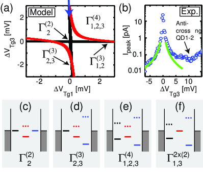
Although the anti-crossing is not resolved in our device, second or higher order cotunneling can be discussed in terms of elastic cotunneling rates , where is the order and is the QD(s) in Coulomb blockade. In the close vicinity of the above discussed crossing, only QD2 is in Coulomb blockade (see Fig. 5(c)), and the major contribution to the current therefore stems from second order cotunneling with rate , yielding a relatively high current. Detuning the electrochemical potential of QD1 (QD3) along the horizontal (vertical) resonance line changes the order of the dominant cotunneling to third order (black arrows in Fig. 5(a)). The electrons now have to cotunnel through two neighboring QDs, i.e., QD2 and QD1 (QD3) as seen in Fig. 5(d) for . The current therefore decreases as illustrated by the peak in Fig. 5(b). The green lines show best fit (using the data for negative ) to the measurement , which is the expected gate-dependence sufficiently far from resonance Flensberg . Here the third order process is dominant and we assume negligible contribution due to the simultaneous change of the electrochemical potential of QD2, when changing . A less good correspondence between the fit and the measurement is observed on the right side of the peak, which might be related to the strong anti-crossing between QD1 and QD2 for positive modifying the gate-dependence. For gate voltages outside the lines (white areas in Fig. 5(a)), all QDs are in Coulomb blockade (Fig. 5(e)). Current is then due to fourth order cotunneling and therefore highly suppressed giving the stable charge configurations in the stability diagrams of Fig. 2(a) and Fig. 3(a). For completeness, one additional type of process exists involving two second order cotunneling corresponding to having only the electrochemical potential of QD2 at resonance (see Fig. 5(f)). This process is more likely than third order cotunneling SchroerPRB consistent with the higher current along sloping lines () than vertical lines () in the double quantum dot (DQD12) stability diagram shown in Fig. 3(a).
In conclusion we have shown measurement on a top-gated single wall carbon nanotube interpreted as a serially coupled triple quantum dot formed between the source and drain electrodes. The stability diagram for single, double and triple quantum dot(s) are observed by individual control of the electron number on each quantum dot via top-gate voltages. An electrostatic model describing ground state transport involving triple quantum dot molecular states captures the main features of the double and triple quantum dot stability diagrams with good agreement. Finally, second order anti-crossings and cotunneling was discussed.
Acknowledgement: We would like to thank Y. Hirayama for support of this joint collaboration and A. Fujiwara and Y. Ono for use of their equipment. Furthermore, we like to acknowledge the support of the EU-STREP Ultra-1D and CARDEQ programs. This work was also supported by the SCOPE from the Ministry of Internal Affairs and Communications of Japan, and by a Grant-in-Aid for Scientific Research from the JSPS.
Supporting Information available: The derivation of the electrostatic energy used in the model is explained in details together with the procedure to obtain stability diagrams without tunnel coupling (S1). Furthermore, the method to include tunnel coupling between neighboring quantum dots yielding the stability diagrams of the triple quantum dot shown in this Letter is addressed (S2).
References
- (1) Sapmaz, S.; Meyer, C.; Beliczynski, P.; Jarillo-Herrero, P.; Kouwenhoven, L. P. Nano Lett. 2006, 6, 1350.
- (2) Loss, D.; DiVincenzo, D. P. Phys. Rev. A 1998, 57, 120.
- (3) van der Wiel, W. G.; de Franceschi, S.; Elzerman, J. M.; Fujisawa, T.; Tarucha, S.; Kouwenhoven, L. P. Rev. Mod. Phys. 2002, 75, 1–22.
- (4) Biercuk, M. J.; Mason, N.; Chow, J. M.; Marcus, C. M. Nano Lett. 2004, 4, 2499.
- (5) Mason, N.; Biercuk, M. J.; Marcus, C. M. Science 2004, 303, 655.
- (6) Biercuk, M. J.; Garaj, S.; Mason, N.; Chow, J. M.; Marcus, C. M. Nano Lett. 2005, 5, 1267.
- (7) Gräber, M. R.; Coish, W. A.; Hoffmann, C.; Weiss, M.; Furer, J.; Oberholzer, S.; Loss, D.; Schönenberger, C. Phys. Rev. B 2006, 74(7), 075427.
- (8) Gräber, M. R.; Weiss, M.; Schönenberger, C. Semicond. Sci. Technol. 2006, 21, 64.
- (9) Jørgensen, H. I.; Grove-Rasmussen, K.; Hauptmann, J. R.; Lindelof, P. E. Appl. Phys. Lett. 2006, 89, 2113.
- (10) Wegewijs, M. R.; Nazarov, Y. V. Phys. Rev. B 1999, 60, 14318.
- (11) Wegewijs, M. R.; Nazarov, Y. V.; Gurvitz, S. A. Jap. J. Appl. Phys. 2001, 40, 1994.
- (12) Waugh, F. R.; Berry, M. J.; Mar, D. J.; Westervelt, R. M.; Campman, K. L.; Gossard, A. C. Phys. Rev. Lett. 1995, 75, 705.
- (13) Waugh, F. R.; Berry, M. J.; Crouch, C. H.; Livermore, C.; Mar, D. J.; Westervelt, R. M.; Campman, K. L.; Gossard, A. C. Phys. Rev. B 1996, 53, 1413.
- (14) Schröer, D.; Greentree, A. D.; Gaudreau, L.; Eberl, K.; Hollenberg, L. C. L.; Kotthaus, J. P.; Ludwig, S. Phys. Rev. B 2007, 76(7), 075306.
- (15) Brandes, T. Phys. Rep. 2005, 408, 315–474.
- (16) Renzoni, F.; Brandes, T. Phys. Rev. B 2001, 64(24), 245301.
- (17) Greentree, A. D.; Cole, J. H.; Hamilton, A. R.; Hollenberg, L. C. Phys. Rev. B 2004, 70(23), 235317.
- (18) Michaelis, B.; Emary, C.; Beenakker, C. W. J. Europhys. Lett. 2006, 73, 677.
- (19) Emary, C. Phys. Rev. B 2007, 76, 245319.
- (20) Meier, F.; Levy, J.; Loss, D. Phys. Rev. B 2003, 68(13), 134417.
- (21) Zhang, P.; Xue, Q.-K.; Zhao, X.-G.; Xie, X. C. Phys. Rev. A 2004, 69(4), 042307.
- (22) Gaudreau, L.; Studenikin, S. A.; Sachrajda, A. S.; Zawadzki, P.; Kam, A.; Lapointe, J.; Korkusinski, M.; Hawrylak, P. Phys. Rev. Lett. 2006, 97(3), 036807.
- (23) Korkusinski, M.; Puerto Gimenez, I.; Hawrylak, P.; Gaudreau, L.; Studenikin, S. A.; Sachrajda, A. S. Phys. Rev. B 2007, 75, 115301.
- (24) Ihn, T.; Sigrist, M.; Ensslin, K.; Wegscheider, W.; Reinwald, M. New Journal of Physics 2007, 9, 111.
- (25) Stopa, M. Phys. Rev. Lett. 2002, 88(14), 146802.
- (26) Vidan, A.; Westervelt, R. M.; Stopa, M.; Hanson, M.; Gossard, A. C. Appl. Phys. Lett. 2004, 85, 3602.
- (27) Saraga, D. S.; Loss, D. Phys. Rev. Lett. 2003, 90(16), 166803.
- (28) Žitko, R.; Bonča, J.; Ramšak, A.; Rejec, T. Phys. Rev. B 2006, 73(15), 153307.
- (29) Javey, A.; Guo, J.; Wang, Q.; Lundstrom, M.; Dai, H. Nature 2003, 424, 654.
- (30) Kim, W.; Javey, A.; Tu, R.; Cao, J.; Wang, Q.; Dai, H. Appl. Phys. Lett. 2005, 87, 3101.
- (31) Babić, B.; Furer, J.; Iqbal, M.; Schönenberger, C. In Kuzmany, H., Roth, S., Mehring, M., Fink, J., Eds., American Institute of Physics Conference Series, Vol. 723 of American Institute of Physics Conference Series, pages 574–582, 2004.
- (32) Ilani, S.; Donev, L. A. K.; Kindermann, M.; McEuen, P. L. Nature Physics 2006, 2, 687.
- (33) Bruus, H.; Flensberg, K.; Many-body Quantum Theory in Condensed Matter Physics: An Introduction, Oxford University Press, 2004.