Andreev-Klein reflection in graphene ferromagnet-superconductor junctions
Abstract
We show that Andreev reflection in a junction between ferromagnetic (F) and superconducting (S) graphene regions is fundamentally different from the common FS junctions. For a weakly doped F graphene with an exchange field larger than its Fermi energy , Andreev reflection of massless Dirac fermions is associated with a Klein tunneling through an exchange field p-n barrier between two spin-split conduction and valence subbands. We find that this Andreev-Klein process results in an enhancement of the subgap conductance of a graphene FS junction by up to the point at which the conductance at low voltages is greater than its value for the corresponding non-ferromagnetic junction. We also demonstrate that the Andreev reflection can be of retro or specular types in both convergent and divergent ways with the reflection direction aligned, respectively, closer to and farther from the normal to the junction as compared to the incidence direction.
pacs:
74.45.+c, 73.23.-b, 85.75.-d, 74.78.NaTransmission of low energy electrons through a normal-metal -superconductor (NS) junction is realized via a peculiar scattering process, known as Andreev reflection (AR) andreev . In AR an electron excitation with energy and spin direction upon hitting the NS-interface is converted into a hole excitation with the same energy but opposite spin direction . Under AR the momentum change is of order which is negligibly small for a degenerate N metal with large Fermi energy . Thus the hole velocity is almost opposite to the velocity of the incident electron (since a hole moves opposite to its momentum), which implies that Andreev process is retro reflection. Andreev reflection results in a finite conductance of a NS junction at the voltages below the superconducting gap BTK .
The fact that the Andreev reflected electron-hole belong to different spin-subbands has an important consequence for Andreev conductance when N metal is a ferromagnet (F). The exchange splitting energy of F-metal induces an extra momentum change of the reflected hole which diminishes the amplitude of AR. As the result the subgap Andreev condutance of ferromagnet-superconductor (FS) junctions decreases with increasing and vanishes for a half-metal F with beenakker95 . Suppression of AR at FS interface is a manifestation of the common fact that ferromagnetism and spin singlet superconductivity are opposing phenomena. In this letter, however, we show that the situation differs significantly if the FS junction is realized in graphene, the recently discovered two-dimensional (2D) carbon atoms arranged in hexagonal lattice geim04 ; geim05 ; kim05 . We find that in a graphene FS junction, the exchange interaction can enhance the subgap Andreev conductance, depending on the doping of F graphene. In particular we show that at low voltage the conductance of a graphene FS junction with a strong exchange field is larger than its value for the corresponding NS structure. We explain this effect in terms of Andreev-Klein reflection in which the superconducting electron-hole conversion at FS interface is accompanied with a pseudo-relativistic Klein transmission through an exchange built p-n barrier between the two spin-split conduction and valence subbands.
Graphene is a zero-gap semiconductor with its conical valnce and conduction bands touching each other at the corners of hexagonal first Brillouin zone, known as Dirac points. The carrier type, (electron-like (n) or hole-like (p)) and its density can be tuned by means of electrical gate or doping of underlying substrate. Due to the connection between this specific band structure and the pseudo-spin aspect which characterizes the relative amplitude of electron wave function in two trigonal sublattices of the hexagonal structure, the charge carriers in graphene behave like 2D massless Dirac fermions with a pseudo-relativistic chiral property wallace ; slonczewski ; haldane ; geim05 ; kim05 . Currently intriguing properties of graphene, which arise from such a Dirac like spectrum, have been the subject of intense studies castro-rmp ; geim07 ; katsnelson07 .
Among others, peculiarity of Andreev reflection in graphene NS junctions was predicted by Beenakker beenakker06 ; beenakker07 . S region with high carrier density can be produced by depositing superconducting electrodes on top of a graphene sheet heersche . It was demonstrated that unlike the highly doped graphene or a degenerate N metal, for undoped graphene with the change in the momentum upon AR could be of order of the momentum of the incident electron. In this limit the dominant process is AR of an electron from the conduction band into a hole in the valence band in which the reflection angle (versus the normal to the NS interface) is inverted with respect to the incidence angle, making Andreev process a specular reflection. Transition from retro reflection at to specular AR at is associated with an inversion of the voltage dependence of the subgap Andreev conductance.
Recently proximity induced ferromagnetism was experimentally realized in graphene spin-valve structures vanwees . Intrinsic ferromagnetic correlations were also predicted to exist in graphene sheets peres and nanoribbons louie . For a pure F graphene sheet the exchange energy shifts the normal Fermi level at Dirac point () upward (downward) by in its spin-up (down) subband. A important consequence of the gapless Dirac spectrum is that this shift makes the up and down spin carriers to be electron-like (n type) and hole-like (p type), respectively peres . Concerning the transport between up and down spin-subbands the exchange field, thus, operates as a p-n potential barrier. The similar situation happens for a doped F graphene () samples with large exchange energies (see the right inset in Fig. 2). At a graphene FS interface AR converting electron-hole from different spin subbands will bring this exchange correlations built p-n barrier into effect. Already reflectionless transmission of chiral electrons through wide and high normal graphene p-n barriers was demonstrated ando98 ; cheianov ; katsnelson ; beenakker08 . This effect called Klein tunneling is analogous to the corresponding effect in quantum relativistic theory klein . We show that the spin Klein tunneling at graphene FS junction leads to an enhancement of the amplitude of AR and the resulting Andreev conductance by the exchange field. This finding specific to graphene is in striking contrast to the behaviour of Andreev conductance of a FS junction in the ordinary metals.
Concerning the connection between the incidence and reflection directions, we further demonstrate variety of Andreev processes taking place in graphene FS junctions. For an incident spin- electron with the velocity direction angle versus the normal to the junction, Andreev reflection can be of retro or specular types indicated, respectively, with or without a sign change in the reflection angle, , in both convergent and divergent ways. The type of AR depends on the ratio , the spin and energy of the incident electron.
We consider a wide graphene FS junction normal to -axis with ferromagnetic region for and highly doped superconducting region for . In the F region the two up and down () spin subbands are split by , such that the spin excitation spectrum versus 2D wave vector is give by
| (1) |
where the two branches of the spectrum originate from the valence and conduction bands, respectively. In S region and the superconducting correlations are characterized by the order parameter which is taken to be real and constant. For calculation we adopt Dirac-Bogoliubov-de Gennes equation beenakker06 which describes the superconducting correlation between massless Dirac fermions with different valley indices. In the presence of an exchange interaction it has the form
| (2) |
where is the Dirac Hamiltonian and the potential energy in S and in F; and are Pauli matrices in the pseudospin space of the sublattices.
Within the scattering formalism we find the spin-dependent amplitude of Andreev and normal reflections from FS interface. An incident spin- electron from left to FS interface with a subgap energy and the incidence angle can be either normally reflected or Andreev reflected as a hole with opposite spin along the reflection angle . Denoting the amplitude of normal and Andreev reflections, respectively, by and the wave function inside F is written as where and are the eigenstates of Hamiltonian (2) in F. The transmitted part of the electron into S, consists of two superconducting quasiparticles whose wave functions decay exponentially as a function of (). Matching the wave functions in F and S at the interface we obtain
| (3) | |||
| (4) |
From the conservation of the -component wave vector under the scattering we obtain the following relation between the incidence and reflection angles
| (5) |
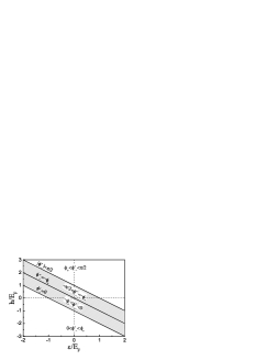
Inspection of the results given by Eqs. (1) and (3)-(5) reveals variety of spin-dependent Andreev processes in the FS graphene junction. Consider an spin-up electron with the energy above the Fermi level in the conduction band () hitting the junction in an angle versus the normal to the junction (negative -axis). It can be Andreev reflected as a hole with the same energy below the Fermi level in down-spin subband. From relation (1) we see that as long as the hole is in the conduction band too, and AR is retro. Upon AR and are conserved but the magnitude of the momentum is changed by (see Eq. (1)). These conditions result in the relation for the -component of the down spin hole which shows that above the critical angle , the hole wave function is evanescent and amplitude of AR vanishes. When , and the -component of the reflected hole is the same as the incident electron, so . This defines a line in the phase space of and (see Fig. 1) on which AR is perfectly (incidence and reflection directions are aligned) retro. For a fixed , increasing results in an increase in , implying a divergent retro reflection (see Eq. (5)). As approaches the angle and simultaneously decreases monotonically to approach zero. This implies that close to the line only normally incident spin-up electrons have a finite AR amplitude. Thus in phase diagram shown in Fig. 1 the region between two lines and defines the phase of divergent retro AR. Increasing further we cross the line which is associated with a sign change in the reflection angle from to implying a transition to the regime of specular AR. For higher , decreases toward and increases. In the limit of , and AR becomes perfectly specular. This defines the region of divergent specular AR above the line .
In a similar way we observe that starting from the perfectly retro AR line and decreasing for a fixed , AR remains retro but becomes convergent with . The retro convergent region extends between the two lines of and . Approaching the line , . Upon crossing this line we again will have a retro to specular transition, but this time in a continues way at . Below the line of , is the region of convergent specular AR with . For all convergent reflection region . Note that at zero energy the retro or specular (depending on ) AR will transform from divergent to convergent or vice versa upon changing the spin direction of the incident electron (see Fig. 1).
We have calculated the Andreev conductance of FS junction at zero temperature via Blonder-Tinkham-Klapwijk formula
| (6) |
where the spin- normal-state conductance and the density of states ( is width of the junction).
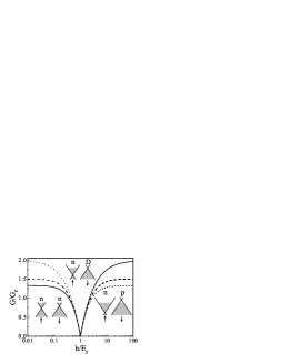
Dependence of the resulting Andreev conductance () on is presented in Fig. 2 for three different bias voltages and for highly doped F graphene . For the conductance decreases monotonically below the corresponding NS value with and vanishes at . In this regime the up and down spin subbands are of the same n type (left inset of Fig. 2) and the effect of exchange field is to impose a normal barrier against AR. The resulting momentum difference of Andreev reflected electron-hole diminishes AR amplitude and hence the Andreev conductance. At the down spin subband is at Dirac point (middle inset of Fig. 2) with a vanishing density of states which results in . For Fermi level of spin down electrons is transferred into the valence band and thus the exchange field barrier finds a p-n characteristic with the height (right inset of Fig. 2). In this case the conductance increases monotonically with . In the limit of the exchange barrier transforms to an almost perfect p-n barrier with the height which makes possible perfect transmission of chiral Dirac fermions between the two subbands. The enhancing Andreev conductance reaches a limiting maximum which depends on the bias voltage. Importantly we see that at this limiting value is larger than the value for corresponding NS structure as shown in Fig. 2. This effect is in contrast to the common view that that ferromagnetic ordering and the singlet superconductivity are exclusive phenomena.
Finally, we note that with the recent successful induction of superconductivity heersche and spin-polarization vanwees in graphene sheets, realizing graphene FS junctions seems feasible. This will allow for the experimental observation of the above predicted effect.
In conclusion, we have demonstrated the unusual features of Andreev reflection in graphene ferromagnet-superconductor junctions. We have shown that depending on the ratio of the exchange field and Fermi energy in F graphene and the energy and spin direction of the incident electron, the Andreev reflection may be of retro or specular types with possibility of being convergent as well as divergent. More fundamentally and in contrast to the common view, we have found that for the exchange field enhances the Andreev conductance of FS junction to reach a maximum value which at low bias voltages is greater that its value for the corresponding non-ferromagnetic structure. We have explained this effect in terms of Andreev-Klien reflection in which the superconducting electron-hole conversion at FS interface is associated with a Klein tunneling through the exchange built p-n barrier between the spin-split conduction and valence subbands.
References
- (1) A. F. Andreev, Sov. Phys. JETP 19, 1228 (1964).
- (2) G. E. Blonder, M. Tinkham, and T. M. Klapwijk, Phys. Rev. B 25, 4515 (1982).
- (3) M. J. M. de Jong and C. W. J. Beenakker, Phys. Rev. Lett. 74, 1657 (1995).
- (4) K. S. Novoselov et al., Sience 306, 666 (2004).
- (5) K. S. Novoselov et al., Nature 438, 197 (2005).
- (6) Y. Zhang, Y. W. Tan, H. L. Stormer, and P. Kim, Nature 438, 201 (2005).
- (7) P. R. Wallace, Phys. Rev. 71, 622 (1947).
- (8) J. C. Slonczewski and P. R. Weiss, Phys. Rev. 109, 272 (1958).
- (9) F. D. M. Haldane, Phys. Rev. Lett. 61, 2015 (1988).
- (10) A. H. Castro Neto, F. Guinea, N. M. R. Peres, K. S. Novoselov, and A. K. Geim, arXiv:0709.1163 (2007).
- (11) A. K. Geim and K. S. Novoselov, Nature Mat. 6, 183 (2007).
- (12) M. I. Katsnelson and K. S. Novoselov, Solid State Comm. 143, 3 (2007).
- (13) C. W. J. Beenakker, Phys. Rev. Lett. 97, 067007 (2006).
- (14) C. W. J. Beenakker, arXiv:0710.3848 (2007).
- (15) H. B. Heersche et al., Nature 446, 56 (2007).
- (16) N. Tombros et al., Nature 448, 571 (2007).
- (17) N. M. R. Peres, M. A. N. Araújo, and D. Bozi, Phys. Rev. B 70, 195122 (2004); N. M. R. Peres, F. Guinea, and A. H. Castro Neto, Phys. Rev. B 72, 174406 (2005).
- (18) Y. -W. Son, M. L. Cohen, and S. G. Louie, Nature 444, 347 (2006).
- (19) T. Ando, T. Nakanishi, and R. Saito, J. Phys. Soc. Japan 67, 2857 (1998).
- (20) V. V. Cheianov and V. I. Fal’ko, Phys. Rev. B 74, 041403(R) (2006).
- (21) M. I. Katsnelson, K. S. Novoselov, and A. K. Geim, Nature Phys. 2, 620 (2006).
- (22) C. W. J. Beenakker, A. R. Akhmerov, P. Recher, and J. Tworzydlo, Phys. Rev. B 77, 075409 (2008).
- (23) O. Klein, Z. Phys. 53, 157 (1929).