Enhancement of optical switching parameter and third-order optical
nonlinearities in embedded Si nanocrystals:
a theoretical assessment
Abstract
Third-order bound-charge electronic nonlinearities of Si nanocrystals (NCs) embedded in a wide band-gap matrix representing silica are theoretically studied using an atomistic pseudopotential approach. Nonlinear refractive index, two-photon absorption and optical switching parameter are examined from small clusters to NCs up to a size of 3 nm. Compared to bulk values, Si NCs show higher third-order optical nonlinearities and much wider two-photon absorption threshold which gives rise to enhancement in the optical switching parameter.
keywords:
Third-order nonlinearities , Embedded nanocrystals , Optical switching parameterPACS:
42.65.-k , 42.65.Ky , 78.67.BfBoth the subjects of Si nanocrystals (NCs) and nonlinear optics are currently very active because of their well established applications, such as those in light emitting diodes, lasers, solar cells, interferometers, optical switches, optical data storage elements, and other photonic devices [1]. One group of very important optical nonlinearities is the third-order nonlinearities which involve nonlinear refraction coefficient or optical Kerr index and two-photon absorption coefficient . These nonlinearities are crucial in all-optical switching and sensor protection applications [2] as well as in the up-conversion of the sub-band-gap light for the possible solar cell applications [3]. In these respects, a clear understanding of the third-order nonlinearities in Si NCs would play an important role in such applications.
Si NCs with controllable sizes have electronic structure largely affected by the quantum and dielectric confinements. Hence, they are expected to have markedly different nonlinear optical properties with respect to bulk Si which itself already displays significant third-order optical nonlinearities [4, 5]. In fact, recent experimental reports show that Si NCs have promising nonlinear optical properties and device applications [6, 7, 8]. Therefore, an in-depth knowledge of Si NCs’ nonlinear parameters is essential for various nonlinear optics applications. Unfortunately, there is neither a comprehensive theoretical work nor an experimental study on the full wavelength and size dependence of the third-order optical nonlinearities of Si NCs. Among the few available experimental studies, we should mention the work of Prakash et al. in which and were measured [6]. However these measurements were performed at a single wavelength. For a more comprehensive understanding, a rigorous theoretical work is highly required that can also unambiguously extract the NC size effects which is not precise in the experimental studies due to limitations in size control in embedded NCs.
In this paper, our aim is to present such a theoretical assessment of the third-order nonlinearities in Si NCs resolving the size scaling and the full wavelength dependence up to UV region. In this respect, we indiscriminately consider both nonresonant and resonant nonlinearities. Furthermore, unlike most of the previous theoretical studies on linear optical properties which considered hydrogen-passivated NCs, we deal with Si NCs embedded in a wide band-gap matrices representing silica which is the most common and functional choice in the actual structures [1]. The source of optical nonlinearity in this work is the bound (confined) electronic charge of the NC valence electrons filling up to the highest occupied molecular orbital. Especially for ultrafast applications in the transparency region this is the dominant contribution [9].
The characterization of the third-order nonlinear susceptibilities up to a photon energy of 4 eV brings a challenge for the electronic structure. For this purpose we resort to the so-called linear combination of bulk bands basis within the pseudopotential framework [10]. This can handle thousands-of-atom systems both with sufficient accuracy and efficiency over a large energy window which becomes a major asset for the third-order nonlinear optical susceptibilities with very demanding computational costs of their own. Further credence for this particular computational framework is recently established from successful applications of quantum phenomena taking place over several eV energy range, such as the excited-state absorption [11] and the Auger and carrier multiplication [12] in embedded Si and Ge NCs. As our primary interest is on the nonlinear optical properties, we refer to our previous work for further details on the electronic structure [11]. However, some information regarding the embedding host matrix would be in order. In real applications, the common choice is silica [1]. On the other hand, to avoid complications arising from its chemical and structural compositions, we prefer to replace it with an artificial medium having the same crystal structure as silicon but possessing the band alignment and refractive index compatible with SiO2. Both of these are crucial for the accurate representation of the quantum and dielectric confinement of the actual system.
In this work, the electromagnetic interaction term in the Hamiltonian is taken as , in other words, the length gauge is used. The third-order optical nonlinearity expressions based on the length gauge have proved to be successful in atomic-like systems [2]. Therefore, we use the expressions based on the length gauge whose detailed forms can be found in Ref. [13]. For embedded NCs an important parameter is the volume filling factor of the NCs where and are the volumes of the NC and the (computational) supercell, respectively. Throughout this work, for the sake of generality the nonlinear properties of the embedded NC systems are calculated at the unity filling factor which is indicated by an overbar
| (1) |
where the subscripts refer to cartesian indices, , , and are the input frequencies, . Our results can trivially be converted to any specific filling factor. As we consider only spherical NCs, we set the cartesian tensor indices as = and suppress these subscripts for convenience. Furthermore, we use a Lorentzian energy broadening parameter of 100 meV at full width. The value refers to the typical room temperature photoluminescence (hence, interband) linewidth of a single Si NC embedded in SiO2 as considered in this work [14]. This parameter not only broadens the resonances but also introduces the band tailing effects [15] which becomes especially important in the transparency regions.
At high illumination intensities, third-order changes in the refractive index and the absorption are observed due to the virtual and real excitations of the bound charges. Accounting for these effects, the refractive index and the absorption become, respectively, and , where is the linear refractive index, is the linear absorption coefficient, and I is the light intensity. and are proportional to and , respectively [16]. Furthermore, the degenerate two-photon absorption cross section [2] at unity filling factor is given by ; and are related to each other through .
In the case of NCs, one should take into account the local field effects (LFEs) as in composite materials the dielectric mismatch between the constituents may lead to remarkably different optical properties [17]. Incorporation of the LFEs into calculations is not a trivial task. For structures of the so-called Maxwell-Garnett geometry [17], the LFEs yield the following correction factor for the third-order nonlinear optical properties [17]
| (2) |
where and are the dielectric functions of the host matrix and the NC, respectively. Note that in this equation it is assumed that the inclusions are non-interacting spheres and the host matrix does not show any significant nonlinearity [18]. In our implementation we use a static local field correction, otherwise the correction factor spuriously causes negative absorption regions at high energies. Further theoretical work is much needed in this direction. Regarding the other shortcomings of our model, we would like to mention that our treatment does not include the excitonic, strain, thermal and free-carrier effects, which may form the basis of possible extensions of this work. Nevertheless, we can argue that in our context the lack of these effects will not have qualitative consequences. First of all regarding the strain, a very recent and realistic atomistic modeling of this system has revealed that the inner core of the NCs where most wave function localization occurs remains unstrained [19]. As for the thermal effects, in this work they are indirectly accounted through the Lorentzian broadening parameter which is predominantly caused by the low energy acoustic phonons [20]. On the other hand, the free-carrier, phonon-assisted or other thermal nonlinearities are totally left out of the scope of our treatment which focuses on the bound-charge nonlinearities taking place in much faster time scale. Finally, the excitonic effects may introduce new features to the spectra, however, at room temperature we do not expect them to markedly stand out.
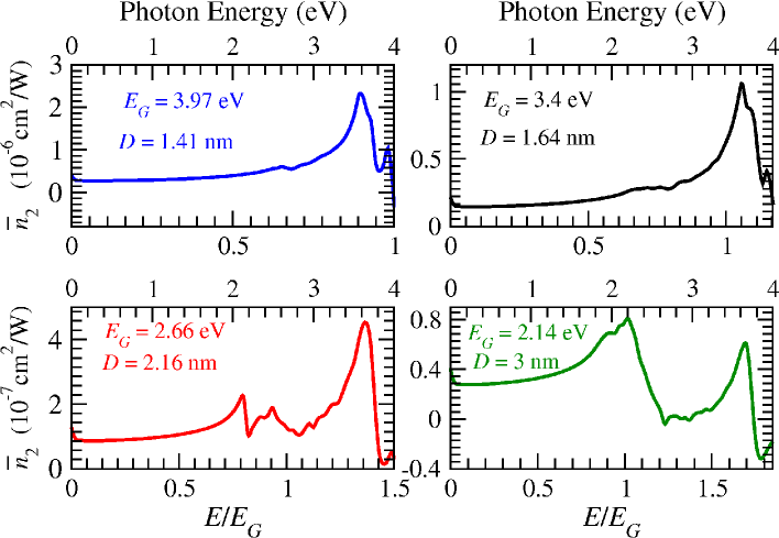
We consider four different diameters, 1.41, 1.64, 2.16 and 3 nm. Their energy gap as determined by the separation between the lowest unoccupied molecular orbital (LUMO) and the highest occupied molecular orbital (HOMO) energies show the expected quantum size effect [11]. The is plotted in Fig. 1 which increases with the decreasing NC size for all frequencies. The smallest diameter gives us the largest . When compared to the of bulk Si in this energy interval ( cm2/W) [4, 5, 21], our calculated is enhanced as much as () for the largest NC. For Si NCs having a diameter of a few nanometers, Prakash et al. [6] have obtained of the order of cm2/W which in order of magnitude agrees with our results when a typical is assumed for their samples.
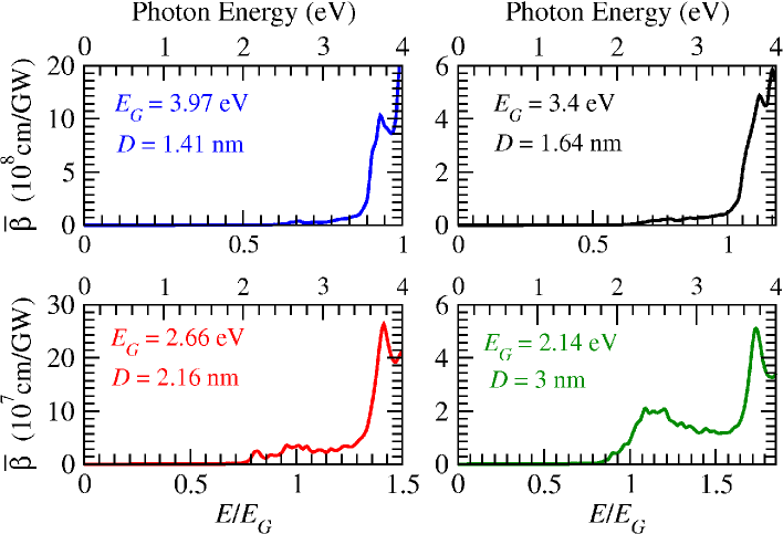
We have plotted against the photon energy in Fig. 2. Peaks at high energies are dominant in the spectrum and decreases with the growing NC volume. The obtained is about cm/GW for the largest NC at around 1 eV. When compared to the experimental bulk value ( cm/GW measured at around 1 eV) [4], our calculated is enhanced about times. Prakash et al [6] have observed to be between ( cm/GW) at eV which is close to our values provided that is taken into account. Moreover, at eV in our results (not shown) is enhanced with the decreasing volume. This is in full agreement with the findings of Prakash et al [6]. However, the result of the composite material was given in this experiment rather than the contributions of each constituent, that is, the host matrix and Si NCs.
We should note that is nonzero down to static values due to band tailing as mentioned above. Another interesting observation is that the two-photon absorption threshold is distinctly beyond the half band gap value, which becomes more prominent as the NC size increases. This can be explained mainly as the legacy of the NC core medium, silicon which is an indirect band-gap semiconductor. Hence, the HOMO-LUMO dipole transition is very weak especially for relatively large NCs. We think that this is the essence of what is observed also for the two-photon absorption. As the NC size gets smaller, the HOMO-LUMO energy gap approaches to the direct band-gap of bulk silicon, while the HOMO-LUMO dipole transition becomes more effective.
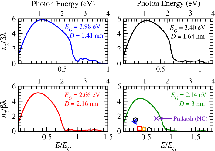
In optical switching systems has an important role [2]. A good optical switching device should possess the condition where is the change in the refractive index and is a constant of the order of unity, the exact value of which depends on the switching system [9]. For the energies below the band gap, one has and . In this case, the condition reduces to . We have plotted this optical swicthing parameter as a function of the photon energy in Fig. 3. Their general behavior resembles the results of Khurgin and Li for the third-order intersubband nonliearities in quantum wells [22].
The condition gives us values already exceeding unity and it brings about an immediate peak at around eV for each diameter. We should note that this is not the case for bulk Si which shows a monotonic behavior, as computed by Dinu for the phonon-assisted two-photon absorption [23]. It can be also observed from this figure that the peak positions are red-shifted with the increasing NC volume. Notably, the switching condition gives higher values as the NC gets smaller, but it converges to a specific value and does not get enhanced further. In the same figure some experimental data for the bulk Si [4, 5, 21] and Si NC with nm [6] are also shown. Note that the experimental result for Si NCs [6] is higher than the bulk values. Our result for the NC with nm is in good agreement with the experimental NC value. Our calculations lie even above the experimental ones. However, we think that a better agreement will be obtained when the experiments are held at a broad range of laser wavelengths. As a result, the calculations show that Si NCs access large values of the ratio , particularly at small NC volumes. This feature should be taken into account in assessing Si NCs for nonlinear device applications especially for optical switching systems [9, 22].
In summary, we have investigated the wavelength and size dependence of the bound-charge third-order optical nonlinearities in Si NCs. It is observed that both and are enhanced with the decreasing of the NC size, giving values greater than their respective bulk values. Finally, optical switching parameter is assessed based on the numerical results. Si NCs enhance this parameter with respect to bulk Si.
Acknowledgments
This work has been supported by the European Commission’s FP6 Project SEMINANO
under Contract No. NMP4-CT2004-505285 and by the Scientific and Techological Research
Council of Turkey, TÜBİTAK under the BİDEB Programme and
with the Project No. 106T048.
References
- [1] L. Pavesi and D.J. Lockwood, Silicon Photonics, Springer, Berlin, 2004.
- [2] R.W. Boyd, Nonlinear Optics, Academic Press, San Diego, 2003.
- [3] T. Thurpke, M.A. Green, and P. Würfel, J. Appl. Phys. 92 (2002) 4117.
- [4] A.D. Bristow, N. Rotenberg, and H.M. van Driel, Appl. Phys. Lett. 90 (2007) 191104.
- [5] Q. Lin, J. Zhang, G. Piredda, R.W. Boyd, P.M. Fauchet, and G.P. Agrawal, Appl. Phys. Lett. 91 (2007) 021111.
- [6] G.V. Prakash, M. Cazzanelli, Z. Gaburro, L. Pavesi, F. Iacona, F. Franzo, and J.G. Priolo, J. Appl. Phys. 91 (2002) 4607.
- [7] L. Pavesi, Z. Gaburro, L. Dal Negro, P. Bettotti, G.V. Prakash, M. Cazzanelli, and C.J. Oton, Optic Las. Eng. 39 (2003) 345.
- [8] S.M. King, S. Chaure, J. Doyle, A. Colli, A.C. Ferrari, and W.J. Blau, Opt. Commun. 276 (2007) 305.
- [9] M. Sheik-Bahae, D.C. Hutchings, D.J. Hagan, and E.W. Van Stryland, IEEE J. Quantum Electron. 27 (1991) 1296.
- [10] L.W. Wang, A. Franceschetti, and A. Zunger, Phys. Rev. Lett. 78 (1997) 2819.
- [11] C. Bulutay, Phys. Rev. B 76 (2007) 205321.
- [12] C. Sevik and C. Bulutay, Phys. Rev. B 77 (2008) 125414.
- [13] R.W. Boyd, Nonlinear Optics, p. 173, Academic Press, San Diego, 2003.
- [14] J. Valenta, R. Juhasz, and J. Linros, Appl. Phys. Lett. 80 (2002) 1070.
- [15] P. Lloyd, J. Phys. C: Solid State Phys. 2 (1969) 1717.
- [16] M. Sheik-Bahae, A.A. Said, T.H. Wei, D.J. Hagan, and E.W. Van Styrland, IEEE J. Quantum Electron. 26 (1990) 760.
- [17] J.E. Sipe and R.W. Boyd, Optical Properties of Nanostructured Random Media, in: V. M. Shalev (Ed.), Topics Appl. Phys., vol. 82, Springer, Berlin-Heidelberg, 2002.
- [18] J.E. Sipe and R. W. Boyd, Phys. Rev. A 46 (1992) 1614.
- [19] D. E. Yılmaz, C. Bulutay, and T. Çağın, Phys. Rev. B 77 (2008) 155306.
- [20] I. Sychugov, R. Juhasz, J. Valenta, and J. Linros, Phys. Rev. Lett. 94 (2005) 087405.
- [21] M. Dinu, F. Quochi, and H. Garcia, Appl. Phys. Lett. 82 (2003) 2954.
- [22] J.B. Khurgin and S. Li, Appl. Phys. Lett. 62 (1993) 126.
- [23] M. Dinu, IEEE J. Quantum Electron. 39 (2003) 1498.