Density inhomogeneity driven percolation metal-insulator transition and dimensional crossover in graphene nanoribbons
Abstract
Transport in graphene nanoribbons with an energy gap in the spectrum is considered in the presence of random charged impurity centers. At low carrier density, we predict and establish that the system exhibits a density inhomogeneity driven two dimensional metal-insulator transition that is in the percolation universality class. For very narrow graphene nanoribbons (with widths smaller than the disorder induced length-scale), we predict that there should be a dimensional crossover to the 1D percolation universality class with observable signatures in the transport gap. In addition, there should be a crossover to the Boltzmann transport regime at high carrier densities. The measured conductivity exponent and the critical density are consistent with this percolation transition scenario.
pacs:
71.30.+h,81.05.Uw,73.40.-c,64.60.ahOne of the remarkable experimental findings of the past two years, creating a great deal of activity and controversy, has been the observation that the carrier density dependent dc conductivity of gated 2D graphene layers, while being approximately linear in density at high gate voltage, becomes a non-universal constant over a finite gate voltage range around the charge neutral Dirac point. While this conductivity minimum plateau formation around the charge neutrality point in 2D graphene is experimentally well established Novoselov et al. (2004), the actual values of and are non-universal and depend on the sample quality Tan et al. (2007); Chen et al. (2008). The minimum conductivity plateau in graphene has been theoretically explained Hwang et al. (2007); Adam et al. (2007) to arise from the invariable presence of unintentional random charged impurities at (or near) the graphene-substrate interface which lead to inhomogeneous electron-hole puddle formation in the low gate voltage regime Hwang et al. (2007); Adam et al. (2007); Rossi and Das Sarma (2008). We note that distortions of the graphene membrane and quenched ripples can also give rise to density inhomogeneities Brey and Palacios (2008), and there have been recent theories studying the effect of ripples on graphene conductivity Katsnelson and Geim (2008). While we focus here on charged impurity induced inhomogeneities, many of our conclusions are only sensitive to the existence of the inhomogeneous density landscape (i.e. electron-hole “puddles”), and these do not distinguish between mechanisms (e.g. impurities, ripples) producing these puddles. Since graphene is a 2D semimetal (or more appropriately, a zero-gap 2D chiral semiconductor with electron-hole bands touching each other linearly at the charge neutral Dirac point), the conductivity becomes an approximate constant when the gate voltage induced chemical potential is pinned in this electron-hole puddle region around the Dirac point. This inhomogeneous electron-hole puddle based theoretical understanding of the graphene minimum conductivity plateau formation leads immediately to an important fundamental question: Are there situations where this inhomogeneous puddle picture leads to a graphene 2D metal-insulator transition (2D MIT) as is known Das Sarma et al. (2005); Manfra et al. (2007) to occur in 2D semiconductor systems?
We show in this Letter that indeed, as a direct consequence of the inhomogeneous puddle formation in graphene, the system will manifest a 2D MIT, which is precisely in the same universality class as the corresponding 2D MIT in electron Das Sarma et al. (2005) and hole Manfra et al. (2007) GaAs systems, provided that there is an energy gap separating the graphene electron and hole bands. The fundamental physics here is that of percolation – for usual 2D zero-gap graphene, percolation through the puddles is allowed at all gate voltages, occurring either through the electron puddles or the hole puddles (or through both Cheianov et al. (2007)), since one or the other is always percolating. If there is a gap, however, then there should be a percolation-driven 2D MIT in graphene exactly as found Das Sarma et al. (2005); Manfra et al. (2007) in 2D GaAs based semiconductor structures.
The easiest way to introduce an energy gap in graphene, which would then immediately lead to a percolation-induced transport gap (i.e. two separate 2D MIT transitions for electrons and holes), is to consider graphene nanoribbons instead of bulk 2D graphene. In this Letter, we predict and confirm experimentally that graphene nanoribbons exhibit a 2D MIT in the low carrier density regime as a function of the applied gate voltage and that this MIT is in the percolation universality class; furthermore, we predict theoretically that as ribbons become very narrow, there should be a dimensional crossover to the 1D universality, implying that the observed transport gap would tend to infinity as the ribbon width goes to zero (or in practice, becomes smaller than the typical size of the puddles), reflecting the 1D percolation universality where metallic conduction is completely suppressed. We speculate that such a 2D-1D crossover may have been observed in recent experiments Han et al. (2007); Li et al. (2008), but more quantitative work and more data would be necessary to establish this prediction.
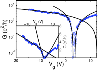
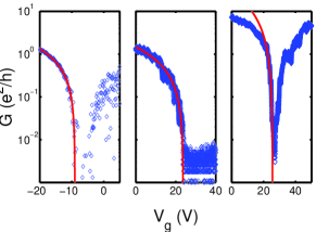
In Fig. 1 we show our experimental data supporting a percolation driven metal-insulator transition on a naturally occurring graphene nanoribbon (that is expected to have smoother edges than comparable ribbons fabricated using the method of Ref. Han et al. (2007)) of dimensions and . The conductance is shown as a function of applied gate voltage . We performed Quantum Hall measurements on the large area connected to the ribbons to confirm that we have a mono-layer of graphene and the details of the fabrication can be found in Ref. Chen et al. (2008). Best fits to Eq. 1 at low density give conductivity exponents and (close to the theoretically expected value ), and the fit to Eq. 2 at high density gives which is consistent with measurements on similarly prepared bulk graphene samples Chen et al. (2008). Fig. 2 shows a similar analysis for a sample fabricated at Maryland, and two of the Columbia samples ( and ) reported in Ref. Han et al. (2007). All three samples show the low-density percolation universality class with critical exponents , and respectively, which are similar to percolation exponents observed in 2D GaAs systems Das Sarma et al. (2005); Manfra et al. (2007). The corresponding fit parameters for the three samples are and respectively, and and respectively (the units of are ).
For the 2D percolation universality class, at low density we have
| (1) |
where is the 2D percolation critical exponent. For graphene ribbons, we expect two such percolation transitions, one for electrons and one for holes, separated by a “transport gap” defined as , where is the critical density for electrons (holes) and is the graphene Fermi velocity. For larger carrier densities, where , we expect a crossover to a high-density Boltzmann transport regime where Hwang et al. (2007); Adam et al. (2007)
| (2) |
just as for bulk graphene on a SiO2 substrate (where is the charge neutrality point and is the surface impurity density of Coulomb scatterers). If we define as the typical size of the electron or hole puddle, where below we calculate self-consistently using the random phase screening approximation, then so long as the sample width , we would have 2D percolation whereas if one has 1D percolation i.e. a chain of approximately p-n junctions. Changing (which could be extracted from high density mobility measurements) would also change and the critical width for which this dimensional crossover is observed. Moreover, we predict that signatures of reduced dimensionality should be apparent in temperature dependent transport measurements.
To date, most theories for transport in graphene nanoribbons consider a quasi 1D, rather than the 2D limit. The experimental observation of 2D percolation in these ribbons casts strong doubt onto the relevance of the quasi 1D theories for current graphene nanoribbon experiments. As was already discussed in Ref. Nakada et al. (1996), many features of the quasi 1D geometry get washed out for which is the case in most experiments on graphene nanoribbons. The length scale controlling the crossover from quasi 1D to 2D behavior in this context may very well be determined by other independent parameters which are unknown at this stage such as the inelastic scattering length or the phase breaking length (both of which depend on temperature). Whether the transport properties in graphene nanoribbons should be considered using a 2D or a quasi 1D Hamiltonian is at this stage an open question requiring further theoretical and experimental study. Our analyses involving data from two groups, our own and that of the Columbia group Han et al. (2007), clearly establish that depending on the value of either the 2D or 1D percolation universality class may apply, where we believe this transition to be controlled by the size of the electron and hole puddles induced by charged impurities. We can not rule out the possibility that further lowering of temperature would lead to quasi 1D behavior Sols et al. (2007) and the percolation-driven 2D MIT is only a crossover phenomenon. Although we focus on single-layer graphene, we note that a similar percolation transition should also be seen in graphene bilayers, where since an electric field induced gap can be introduced into the spectrum without any confinement, the crossover to a quasi 1D regime would not arise. We note that even for bulk graphene, a Boltzmann to percolation crossover could be induced with a magnetic field, where for small field and within the electron-hole puddle model, we expect the p-n resistance to be very low justifying the Boltzmann picture, whereas for large magnetic field, the p-n junction becomes very resistive Cheianov and Fal’ko (2006) inducing a percolation transition. This crossover may have been observed in recent experiments Checkelsky et al. (2008).
To reinforce the point that the 2D MIT in graphene nanoribbons is indeed a percolation transition and not a quantum crossover phenomenon, we calculate the percolation critical density using the non-linear screening argument of Efros Efros (1988) with the basic idea being that the MIT occurs when inhomogeneous density fluctuations created by the charged impurities can no longer be screened by the carriers. This leads to where the random charged impurities of concentration are assumed to be located at a distance from the 2D graphene plane. Taking and , typical values estimated Hwang et al. (2007); Adam et al. (2007); Tan et al. (2007); Chen et al. (2008) from mobility measurements, we get . This is in reasonable agreement with our experimental finding in Figs. 1 and 2. On the other hand, the quantum localization crossover density can be estimated from the Ioffe-Regel criterion , where is the mean-free path, to be for the same and values. Thus, , and our experimental critical density agrees with the percolation critical density, providing further support for a percolation driven insulating transition in graphene.
Experimentally, one can measure three different gaps. In addition to the transport gap discussed above, the temperature dependence of the conductivity minimum gives an activated gap (we performed this measurement on the ribbon, and found which is an order of magnitude smaller than theoretical estimates Yang et al. (2007) of the confinement induced gap), and finally, Ref. Han et al. (2007) reported the source-drain bias required to induce conduction and found the gap to be orientation independent (contrary to the expectation of the quasi 1D theory that is extremely sensitive to whether the edge is zig-zag or armchair). The connection between these three experimental gaps and the theoretical gap in the energy spectrum is beyond the scope of this work, where we focus here only on the transport gap and predict that in the 2D regime, provided that the impurity location is pretty much the same, , where is the high-density mobility in the Boltzmann regime Hwang et al. (2007); Adam et al. (2007); Tan et al. (2007); Chen et al. (2008).
The 2D percolation picture presented above breaks down when the sample width becomes smaller than the typical disorder length scale. Using the self-consistent RPA method of Ref. Adam et al. (2007) we can obtain an integral expression for the potential correlation function which for experimentally relevant parameters can be approximated by
| (3) |
Using , where is the effective dielectric constant that depends on the choice of substrate, we find
| (4a) | |||||
| (4b) | |||||
where for and
| (5a) | |||||
| (5b) | |||||
This notation is chosen to be consistent with Ref. Adam et al. (2007) where the rms density . For typical values of and , we have , which is consistent with the experimentally observed critical width Han et al. (2007). In the 1D limit, there should be no percolation transition, only an activated conduction, and the effective gap should diverge in the limit. From Eq. 4, we can predict the dependence of the puddle size (and therefore the critical width of the dimensional crossover) on experimentally tunable parameters. For example, we predict that cleaner samples (i.e. with a larger high-density mobility) would have larger critical widths and by doping graphene with potassium Chen et al. (2008), thereby changing only , one could tune through this dimensional crossover in a sample of fixed width. Changing the substrate to a high- material like HfO2 (assuming that and remain unchanged) could significantly increase the puddle size, in contrast to suspended graphene Bolotin et al. (2008) where increasing (which decreases the puddle size) is compensated by the lower (which tends to increase the puddle size). In addition, we predict that suspended nanoribbon experiments will have a smaller transport gap due to the order of magnitude higher mobility, but the same critical exponent ; while for nanoribbons with potassium doping of various strengths, increasing should lead to a larger transport gap with no change in .
In conclusion, we have argued theoretically and demonstrated experimentally that a disorder induced, density inhomogeneity driven percolation transition is observable in graphene nanoribbons. We anticipate a crossover to Boltzmann transport at high carrier density and a dimensional crossover for sample widths that are smaller than the disorder induced puddle size. Several features of the experiment including the difference between transport and activation gaps, the large discrepancy between the value of the gap and that predicted by band structure theory as well as there being no orientation dependence of the gap and a critical width below which the dimensional crossover causes a divergence in the transport gap (for an infinite 1D system in the limit) are all explained naturally in this picture. This consistent theoretical picture better captures the physics of nanoribbons than the quasi 1D induced models that have dominated the literature to date. Our discovery of a percolation driven graphene 2D MIT also shows the close conceptual connection between 2D graphene transport and 2D semiconductor transport, and establishes that density inhomogeneities dominate carrier transport in both classes of systems at low enough carrier densities. In bulk 2D graphene, which is a zero-gap semiconductor, this leads to the low-density minimum conductivity plateau, and in graphene nanoribbons (as well as in bilayer graphene with an electric field induced gap), where there is an energy gap between the electron and hole bands, we get the same percolation induced 2D MIT familiar from 2D semiconductor electron Das Sarma et al. (2005) and hole Manfra et al. (2007) systems. For very narrow graphene nanoribbons, which are in the 1D percolation regime, our theory predicts an insulating behavior with an effective infinite energy transport gap at , which may have been observed experimentally Han et al. (2007); Li et al. (2008), by virtue of the absence of a percolation transition in 1D. A fundamental question of considerable significance that remains open in this context is the experimental absence of quantum localization Aleiner and Efetov (2006) which may be observable at much lower temperatures than used experimentally so far.
This work is partially supported by U.S. ONR.
References
- Novoselov et al. (2004) K. S. Novoselov et al., Science 306, 666 (2004).
- Tan et al. (2007) Y.-W. Tan et al., Phys. Rev. Lett. 99, 246803 (2007).
- Chen et al. (2008) J. H. Chen, C. Jang, S. Adam, M. S. Fuhrer, E. D. Williams, and M. Ishigami, Nature Physics 4, 377 (2008).
- Hwang et al. (2007) E. H. Hwang, S. Adam, and S. Das Sarma, Phys. Rev. Lett. 98, 186806 (2007).
- Adam et al. (2007) S. Adam, E. H. Hwang, V. M. Galitski, and S. Das Sarma, Proc. Natl. Acad. Sci. USA 104, 18392 (2007).
- Rossi and Das Sarma (2008) E. Rossi and S. Das Sarma, arXiv:0803.0963v1 (2008); J. Martin, N. Akerman, G. Ulbricht, T. Lohmann, J. H. Smet, K. von Klitzing, and A. Yacobi, Nature Physics 4, 144 (2008); V. Brar, Y. Zhang, C. Girit, A. Zettl, and M. Crommie, unpublished (2008).
- Brey and Palacios (2008) L. Brey and J. J. Palacios, Phys. Rev. B 77, 041403 (2008); E. Kim and A. H. Castro Neto, arXiv:cond-mat/0702562v2 (2007); F. de Juan, A. Cortijo, and M. A. H. Vozmediano, Phys. Rev. B 76, 165409 (2007).
- Katsnelson and Geim (2008) M. I. Katsnelson and A. K. Geim, Phil. Trans. R. Soc. A 366, 195 (2008); I. F. Herbut, V. Juričić, and O. Vafek, Phys. Rev. Lett. 100, 046403 (2008); A. Cortijo and M. A. H. Vozmediano, arXiv:0709.2698v1 (2007).
- Das Sarma et al. (2005) S. Das Sarma et al., Phys. Rev. Lett. 94, 136401 (2005).
- Manfra et al. (2007) M. J. Manfra et al., Phys. Rev. Lett. 99, 236402 (2007).
- Cheianov et al. (2007) V. Cheianov, V. Fal’ko, B. Altshuler, and I. Aleiner, Phys. Rev. Lett. 99, 176801 (2007).
- Han et al. (2007) M. Y. Han, B. Ozyilmaz, Y. Zhang, and P. Kim, Phys. Rev. Lett. 98, 206805 (2007).
- Li et al. (2008) X. Li, X. Wang, L. Zhang, S. Lee, and H. Dai, Science 319, 1229 (2008).
- Nakada et al. (1996) K. Nakada, M. Fujita, G. Dresselhaus, and M. S. Dresselhaus, Phys. Rev. B 54, 17954 (1996).
- Sols et al. (2007) F. Sols, F. Guinea, and A. H. Castro Neto, Phys. Rev. Lett. 99, 166803 (2007); I. Martin and Y. M. Blanter, arXiv:0705.0532v2 (2007).
- Cheianov and Fal’ko (2006) V. Cheianov and V. I. Fal’ko, Phys. Rev. B 74, 041403 (2006).
- Checkelsky et al. (2008) J. G. Checkelsky, L. Li, and N. P. Ong, Phys. Rev. Lett. 100, 206801 (2008).
- Efros (1988) A. L. Efros, Solid State Commun. 67, 1019 (1988).
- Yang et al. (2007) L. Yang, C.-H. Park, Y.-W. Son, M. L. Cohen, and S. G. Louie, Phys. Rev. Lett. 99, 186801 (2007); L. Brey and H. A. Fertig, Phys. Rev. B 73, 235411 (2006).
- Bolotin et al. (2008) K. Bolotin et al., Solid State Commun. 146, 351 (2008).
- Aleiner and Efetov (2006) I. Aleiner and K. Efetov, Phys. Rev. Lett. 97, 236801 (2006).