Electronic Structure and Optical Properties of
Silicon Nanocrystals along their Aggregation Stages
Abstract
The structural control of silicon nanocrystals is an important technological problem. Typically a distribution of nanocrystal sizes and shapes emerges under the uncontrolled aggregation of smaller clusters. The aim of this computational study is to investigate the evolution of the nanocrystal electronic states and their optical properties throughout their aggregation stages. To realistically tackle such systems, an atomistic electronic structure tool is required that can accommodate about tens of thousand nanocrystal and embedding lattice atoms with very irregular shapes. For this purpose, a computationally-efficient pseudopotential-based electronic structure tool is developed that can handle realistic nanostructures based on the expansion of the wavefunction of the aggregate in terms of bulk Bloch bands of the constituent semiconductors. With this tool, the evolution of the electronic states as well as the polarization-dependent absorption spectra correlated with the oscillator strengths over their aggregation stages are traced. The low-lying aggregate nanocrystal states develop binding and anti-binding counterparts of the isolated states. Such information may become instrumental with the maturity of the controlled aggregation of these nanocrystals.
I Introduction
Embedded semiconductor nanocrystals (NCs) can be fabricated by several different techniques such as ion implantation iimp1 ; iimp2 , sputtering sput , plasma enhanced chemical vapor deposition pecvd . However, their structural control is still an important technological problem. During the annealing process, the excess silicon atoms start forming clusters and with their gradual aggregation into nanocrystals, a distribution of sizes and shapes emerges. The annealing temperature and duration determine the degree of the cluster aggregation and eventually the average NC size distribution. Being directly controlled by this distribution pecvd ; brongersma the luminescence properties are intimately affected by this process of NC aggregation driven by atomistic nucleation and growth kinetics heinig . It has been generally demonstrated that the increase in the Si concentration of the substoichiometric silicon oxide films, as well as the annealing temperature lead to larger NCs and hence to the red shift of their luminescence spectra pecvd . However, the experimental studies are hampered by the large size distribution existing in typical samples. The soul of the present work is based on the controlled agglomeration of Si NCs. This is currently not achievable by the PECVD, sputtering or ion implantation techniques all of which are kinetically controlled. One of the most sophisticated fabrication tools for this purpose is the extreme ultraviolet interference lithography solak where silicon-based two-dimensional quantum dot arrays with nanometer size control have been successfully demonstrated.
In this work we tackle the electronic structure and the optical properties of Si NCs along their aggregation stages from a computational point of view. For a realistic account of the aggregation process, an atomistic electronic structure tool is required that can accommodate about tens of thousand nanocrystal and embedding lattice atoms with very irregular shapes. However, currently highly sophisticated ab initio density functional theory-based plane wave approaches can only tackle systems below thousand atoms even with the help of ultrasoft pseudopotentials martin-book . For this purpose, a computationally-efficient pseudopotential-based electronic structure tool is developed that can handle realistic nanostructures based on the expansion of the wavefunction of the aggregate in terms of bulk Bloch bands of the constituent semiconductors. With this tool, the evolution of the electronic states as well as the absorption spectra and in particular the oscillator strengths of transitions of interest over their aggregation stages are traced.
II Theoretical Details
We employ a computationally-efficient pseudopotential-based electronic structure tool that can tackle on the order of tens of thousand atom nanostructures based on the so-called linear combination bulk bands recipe of Wang and Zunger wang97 ; wang99 . The crux of the technique is to expand the wavefunction of the NC in terms of bulk Bloch bands of the constituent semiconductors;
| (1) |
where, is the cell-periodic part of the Bloch states, is the number of primitive cells within the computational supercell, is the expansion coefficient set to be determined and is the constituent bulk material label which points to either the NC core or the embedding media. The atomistic NC Hamiltonian is given by
| (2) |
where is the free-electron mass, is the weight function that usually takes values between 0 to 1 depending on the type of atom at the position (which becomes instrumental especially at the interfaces) and is the screened spherical pseudopotential of atom of the material . We use semiempirical pseudopotentials for Si and Ge taken respectively from Refs. wang94 and saravia . This is one other advantage of this simpler approach over the more accurate ab initio techniques which run into well-known band gap shrinkage due to local density approximation martin-book restoration of which is not straightforward.
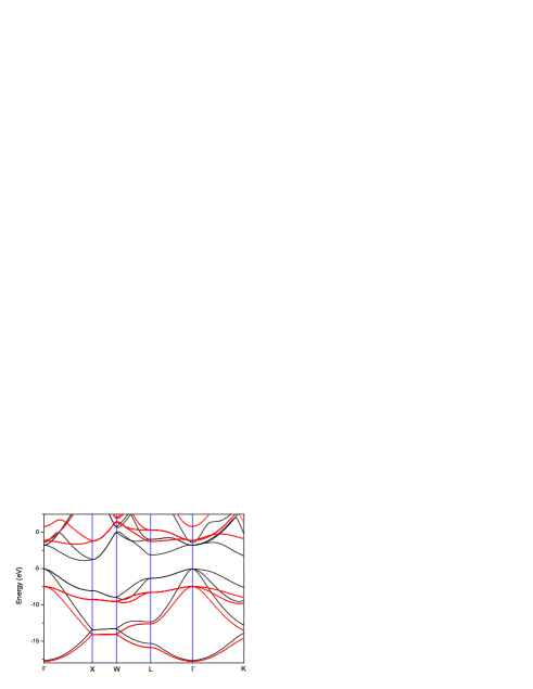
An important issue is the choice of the host matrix material. If the NC is surrounded by vacuum,
this corresponds to the free-standing case. However, the dangling bonds of the surface Si atoms
lead to quite a large number of interface states which adversely contaminate the effective
band gap region of the NC. In reality Si NCs are always embedded into a wide band gap host
matrix which is usually silica sput ; pecvd . For this reason, we embed the Si
NCs into a wide band gap medium having proper band alignment so that both electrons and holes of
Si will experience quantum confinement. This is illustrated in Fig. 1 showing the bulk
band structure of Si and the wide band gap medium with a band gap above 6 eV.
With the possession of the electronic wavefunctions of the NCs, their linear optical properties can be readily computed. Within the independent-particle approximation and the artificial supercell framework weissker the imaginary part of linear dielectric function becomes
| (3) | |||||
where, denotes the cartesian components of the dielectric tensor and
| (4) |
is the oscillator strength of the transition. In these expressions is the volume of the supercell and is the number of points chosen within the Brillouin zone, the label () corresponds to occupied (empty) valence (conduction) band states. Note that implicitly depends on the filling factor which is the ratio of the NC and the supercell volumes. To obtain a more general quantity an effective dielectric function can be introduced as weissker2 . This is the form we prefer to present our results in the next section; for any specific filling factor one can readily infer the corresponding dielectric function. As another technical detail a Lorentzian broadening of 0.2 eV of the Dirac delta function in Eq. (3) is used. Finally, the absorption coefficient is related to the imaginary part of the dielectric function through chuang
| (5) |
This expression is in SI units (unlike the previous expressions) where is the index of refraction, is the speed of light and is the permittivity of free space.
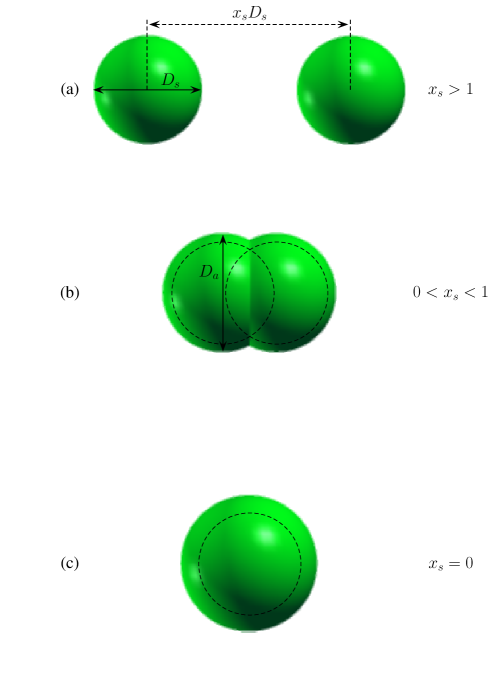
Even though there is no geometrical restriction of the approach, we consider the aggregation of two equal-diameter spherical NCs as illustrated in Fig. 2. Here, the isolated diameters are taken as and the center-to-center distance between the two NCs as . Assuming no strain generation during the aggregation process , the diameter of each NC should expand from to to preserve the overall volume and the number of atoms. A simple geometrical consideration indicates that the expansion factor should be determined by solving the following cubic equation
| (6) |
for a given value that describes the degree of aggregation. This results in some underestimation of the number of atoms due to those lost in the reduced surface area of the aggregate; therefore we slightly enlarge the aggregate size until we accommodate the correct total number of atoms.
III Results
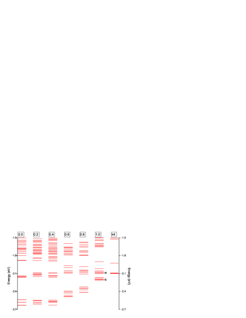
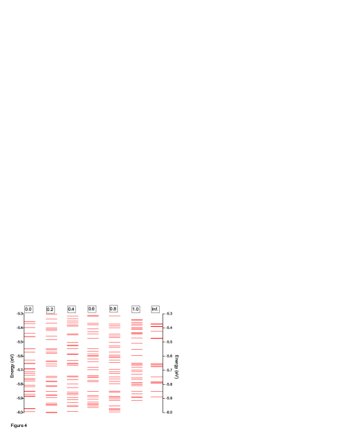
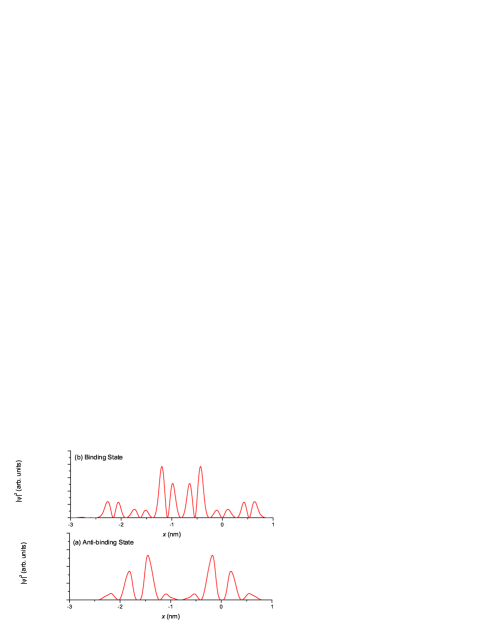
Two NCs each with isolated diameters of 1.6 nm are assumed to approach together along a common axis. The evolution of conduction and valence NC states are shown in Figs. 3 and 4 respectively, with the aggregation being quantified by the parameter. In these scales some of the degeneracies in both the conduction and valence NC states may not be resolved when spherical symmetry is restored for and . However, in intermediate aggregation stages these degeneracies are further lifted. Also note that the conduction NC states are mainly derived from minima of the bulk Si, hence tend to be six-fold degenerate for the low-lying states. Mixing with other bulk band states again lifts the exact degeneracy. From both of these figures, the splitting of the isolated NC states into binding and anti-binding sets can be observed. This is illustrated in Fig. 5 where the wave functions of the two states marked as -a (for anti-binding) and -b (for binding) are plotted clearly justifying their identification.
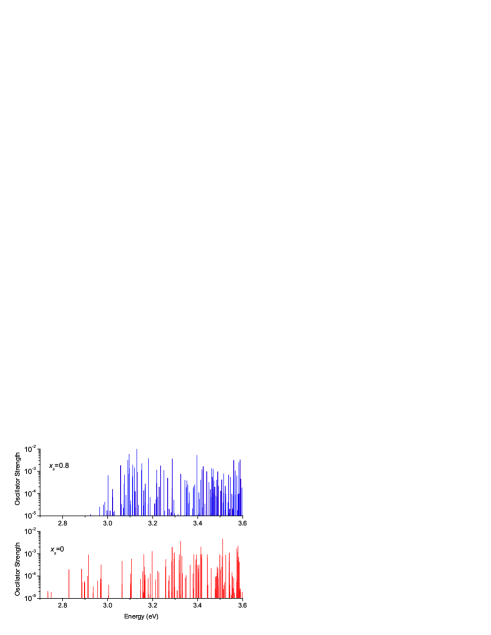
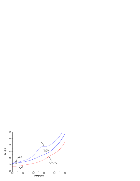
The effect of NC aggregation on the optical properties is shown in Figs. 6 and 7 choosing
and 0 cases for comparison.
We should remark that the embedding medium has no contribution within the energy window
(below 3.6 eV) considered here and all absorption is due to real transitions
between NC states over the effective band gap.
The oscillator strengths are plotted for the component of
the tensor where is the direction along the aggregation. Since the aggregation of the two NCs
leads to a larger NC, transitions are shifted to lower energies, as expected (cf. Fig. 6).
Figure 7 demonstrates that component of the imaginary part of the dielectric function
is enhanced whereas the other two components attain a lower but equal value which is also the
case for the larger and the fully aggregated and spherical case. Note that the energy for
the local peak of the component of the absorption spectra correlates with strong oscillator
strengths in Fig. 6 around 3.15 eV which are absent for .
Obviously, in the case of random growth processes the macroscopic average will wash out such
polarization effects, however for more controlled fabrication techniques may reveal these features.
IV Conclusions
A pseudopotential-based atomistic electronic structure tool is developed to realistically investigate the aggregation process of NCs. With this tool, the evolution of the electronic states as well as the absorption spectra and in particular the oscillator strengths of transitions of interest over their aggregation stages are traced. The predominantly -derived six-pack groupings of conduction NC states are observed. The low-lying aggregate NC states are identified as the binding and anti-binding splittings of the isolated states. The effect of the elongation of the NCs in the initial phases of a controlled aggregation is reflected as a polarization-dependent absorption spectra. Such information may become instrumental with the maturity of the controlled fabrication of these NC aggregates.
Acknowledgements.
This work has been supported by the European FP6 Project SEMINANO with the contract number NMP4 CT2004 505285 and by the Turkish Scientific and Technical Council TÜBİTAK within COST 288 Action.References
- (1) A. Meldrum, R. F. J. Haglund, Jr., L. A. Boatner, and C. W. White, Adv. Mater. (Weinheim, Ger.) 13 (2001) 1431.
- (2) E. S. Marstein, A. E. Gunnæs, U. Serincan, R. Turan, A. Olsen, and T. G. Finstad, Surf. Coat. Tech., 158 (2002) 544.
- (3) S. Hayashi, T. Nagareda, Y. Kanzawa, and K. Yamamoto, Jpn. J. Appl. Phys., 32 (1993) 3840.
- (4) F. Iacona, G. Franzó, C. Spinella, J. Appl. Phys. 87 (2000) 1295.
- (5) M. L. Brongersma, A. Polman, K. S. Min, H. A. Atwater, J. Appl. Phys., 87, (2000) 1295.
- (6) K. H. Heinig, T. Müller, B. Schmidt, M. Strobel, and W. Möller, Appl. Phys. A, 77, (2003) 17.
- (7) H. H. Solak, J. Phys. D: Appl. Phys., 39, (2006) R171.
- (8) R. M. Martin, Electronic Structure, Cambridge University Press, Cambridge, 2004.
- (9) L.-W. Wang, A. Franceschetti, and A. Zunger, Phys. Rev. Lett., 78 (1997) 2819.
- (10) L.-W. Wang and A. Zunger, Phys. Rev. B, 59 (1999) 15806.
- (11) L.-W. Wang and A. Zunger, J. Phys. Chem., 98 (1994) 2158.
- (12) L. S. Saravia and D. Burst, Phys. Rev., 176 (1968) 915.
- (13) H.-Ch. Weissker, J. Furthmüller, and F. Bechstedt, Phys. Rev. B, 65 (2002) 155327.
- (14) H.-Ch. Weissker, J. Furthmüller, and F. Bechstedt, Phys. Rev. B, 65 (2002) 155328.
- (15) S. L. Chuang, Physics of Optoelectronic Devices, Wiley, New York, 1995.