Andreev reflection and spin polarization measurement of Co/YBCO junction
Abstract
We report temperature dependent Andreev reflection measurements of Co/ Y1Ba2Cu3O7-δ (YBCO) heterostructure samples with junction areas of 1 m diameter. Modelling of the 5-70 K conductivity data according to a modified Blonder-Tinkham-Klapwijk theory yields a spin polarization in Co film amounting to 34 which is almost constant up to 70 K. The YBCO films have been grown by pulsed laser deposition on sapphire substrates. The Co films are deposited by thermal evaporation on YBCO. The film is characterized by powder X-ray diffraction measurements which shows YBCO is grown in (001) direction.The critical current density, 5 x 10⁶ A/cm2, in YBCO remains nearly constant after deposition of Co at zero field and 77 K.
keywords:
PACS:
75.50.Pp, 72.25.Dc,72.25.Mk,74.45.+c,
1 Introduction
Andreev reflection experiments across
normal conductor (N) and superconductor (SC) junctions represent
an useful technique to explore various interesting physical properties like spin polarization of ferromagnets, gap anisotropy of superconductors, etc.
Several mechanisms are involved in current transport into superconductor, when a bias voltage V is applied across a clean N/SC point contact.
The electrons can pass from N into SC as
quasielectrons or holes at voltages higher than the superconducting gap , which relax into the Cooper-pair condensate over the charge relaxation distance. However, for
voltages lower than no quasiparticle states are available in the superconductor. Instead, the
current is converted directly into a supercurrent of Cooper
pairs, consisting of two electrons of charge with opposite
spin. This is accomplished by the reflection of a hole back
into the metal, a process first described by Andreev[1].
When a normal metal
is replaced by a ferromagnetic metal (FM), a suppression of Andreev reflection (AR) occurs. For a FM/SC contact the process involves a coherent
interspin-subband transfer which is sensitive to
the relative electronic spin density of states at Fermi energy (). If the spin polarization is zero, the AR is not hindered. However, if amounts to 100 near , there are no spin-down states available
in the metal for the reflected hole and AR is completely suppressed[2, 3]. Hence, determination of for a FM can be
carried out by measuring the suppression of AR.
The spin polarization of a 3-d transition metal FM depends on its electronic structure containing narrow -band and broad -bands at . Co is an interesting 3-d metal with the Curie temperature amounting to 1388 K[4]. Spin-resolved photoelectron spectroscopy measurements showed that Co has short range ferromagnetic order above the Curie temperature[5]. The first experiment
of spin-polarized transport and tunneling in Co was performed by Tedro and
Meservey where was reported to be 34 at 0.4 K [6].
Measurement of by AR spectroscopy is limited by the of the used SC.
Soulen reported = 42 for Co by AR measurements using a Nb tip[2]. Since the superconducting transition temperature () for Nb is around 9 K, was determined only below that temperature.
The resolution
of AR spectroscopy strongly depends on the temperature
due to the broadening of carrier distribution by kBT around the Fermi level. Observation of distinct spectral features requires the condition kBT
kB ( = Debye Temperature) i.e. measurements should be taken at temperatures
considerably lower than the Debye temperature[7].
In order to determine at higher temperature, the necessity of using high-Tc SC as a superconducting electrode for AR measurements is necessary.
A dip in differential conductance of a ferromagnet/high-Tc superconductor junction has been reported as a consequence of suppressed AR[8].
This indicates that the
detection of by AR measurements across FM/high-Tc
superconductor junction should be possible.
Here, we report on AR measurements on Co/YBCO with
junction area of 1 m diameter at 5-100 K. Our analysis and modelling of the sub-gap conductivity variation yields around 34 for Co in the temperature range from 5 to 70 K. To the best of our knowledge, this is the first time that the spin polarization of Co has been probed by Andreev reflection spectroscopy at such elevated temperatures, up to 70 K.
2 Thin film growth and characterization
The investigated YBCO films have been grown
on r-plane oriented sapphire (Al2O3) substrates with
underlying CeO2 buffer layer by pulsed laser deposition (PLD)
technique[9].In general, a large oxygen partial pressure
during the PLD growth of YBCO on sapphire amounting to 0.16 mbar is
required to maintain the stoichiometry of YBCO and to retain its
superconductivity. The deposited thin YBCO films are (001) axis
oriented, orthorhombic in structure and their thickness amounts to
230 30 nm in each sample. The Co/YBCO heterostructure has been
prepared by thermal evaporation of Co on YBCO under a vacuum level of 3 x 10⁻³ mbar.
Thickness of the Co film on YBCO is around 11 nm.
The crystalline quality of the samples
has been investigated by powder X-ray diffraction (XRD) measurements before and after deposition of Co using the Cu-Kα line (= 0.15406 nm).
The XRD spectra of the investigated Co/YBCO heterostructures in Fig. 1
confirm the (001)-axis orientation of YBCO on r-sapphire.
3 Transport experiment
3.1 Critical current density of YBCO
The critical current density () determines the quality of a superconductor. It is essential to probe the
superconductivity of YBCO before and after deposition of Co. We used an inductive method developed to
determine of YBCO films on single-sided or double-sided
sapphire substrates[10]. The magnetic shielding of the
YBCO film is measured in dependence of temperature and AC current in
the measuring coil. The measurement is carried out by placing the
sample into liquid nitrogen to work below YBCO superconduction transition temperature()
amounting to 92 K. We have found that the critical current density
for YBCO amounts to = 3 x 10⁶ A/cm2. The
measurements on Co/YBCO heterostructures
reveal that the critical current density of YBCO remains unchanged. This result proves that the superconductivity of YBCO is preserved after deposition of Co.
3.2 Sample preparation and AR measurements
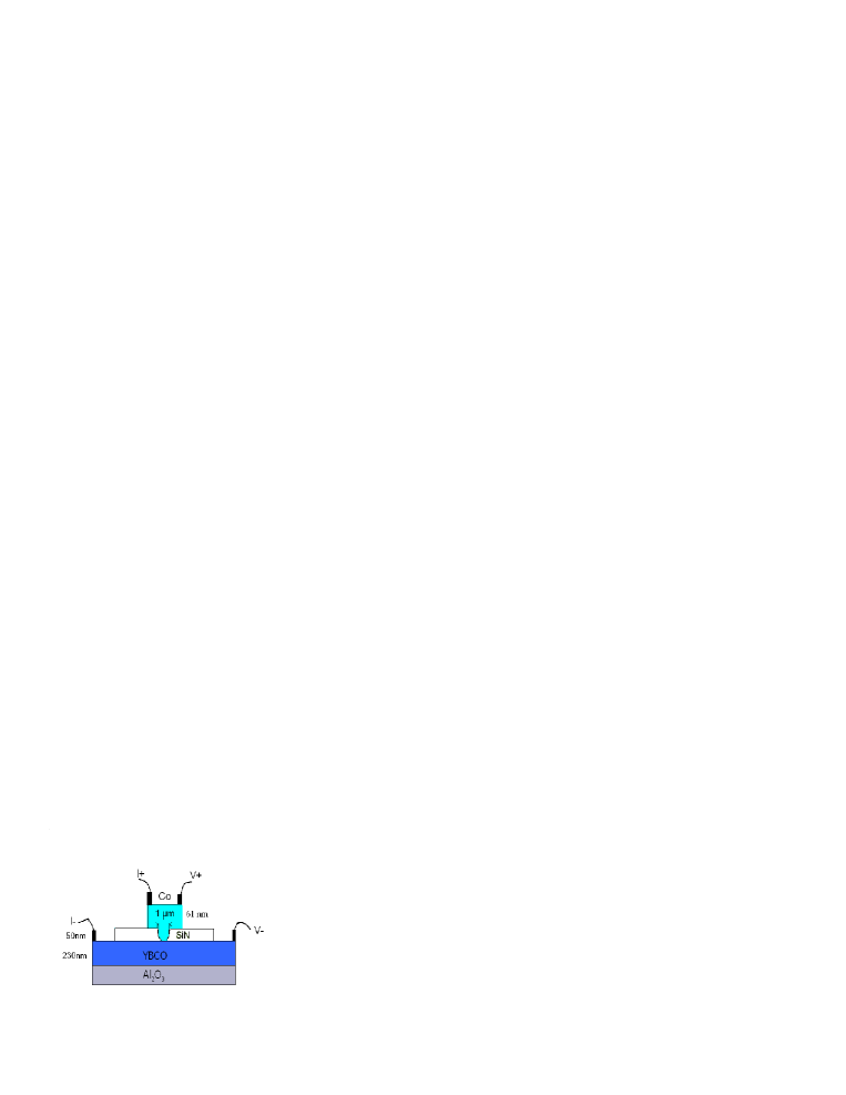
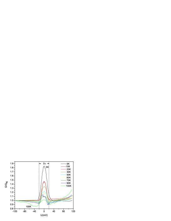
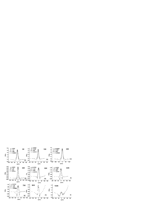
A SiN insulating layer of 50 nm thickness has been deposited on the YBCO film by sputtering deposition method. A single hole of 1 m diameter has been created in SiN by focused ion beam (FIB) etching. The diameter was 1 m at the top of the hole and at the bottom the diameter was much less. Basically, the hole has a conical shape [11]. Hence, the diameter at Co/YBCO contact must be much less than 1 m. Finally, Co films have been deposited on SiN by thermal evaporation. Hence, the Co film on SiN will be about 61 nm thick in the region of the hole. It is known that this kind of hole creation by FIB usually get affected by Gallium (Ga) ion contamination. We have also faced the similar problems and for affected contacts the contact resistance used to be very high. However, we have taken the sample with best contact which has lowest resistance and carried out the AR measurement. The normal contact resistance has been around 16 Kohm. We have calculated the approximate contact area using the formula Gn e2/ k where kF is the Fermi wave vector and the effective contact area () amounts to 0.65 nm2. The measuring electrodes are fabricated by silver paste on the contact pads. Two contacts are made on Co pads, while the other two contacts are made on YBCO pads (Fig. 2). We have carried out current() vs voltage() measurements in four-probe geometry on Co/YBCO samples with junction area of 1 m diameter from 5 to 100 K. The conductivity has been calculated by numerical differentiation of the vs. data. The temperature dependent normalized conductivity data are shown in Fig. 3. We have observed clear Andreev reflection and modelled the data up to 70 K for Co/YBCO samples. Above 70 K it was not possible to model the data because of large background noise.
4 Modelling
We base our analysis and modelling the conductivity data on the pioneering work by Blonder-Tinkham-Klapwijk (BTK) for AR in the ballistic regime [12]. The BTK formula has already been used for a much larger contact area of 1x1 mm2 in Ga0.95Mn0.05As/Ga junctions[13]. Our present Co/YBCO samples have much smaller contact area in the 1 m2 range. The BTK formula is valid for normal metal/-wave superconductor junction. However, in the present investigation, the high-Tc -wave superconductor YBCO has been used[14]. In contrast to -wave superconductor, here the tunneling spectra strongly depend on the tunneling direction with respect to the crystallographic axis. A tunneling theory for normal metal-insulator--wave superconductor has been reported by Tanaka and Kashiwaya [15]. It has been shown by Barash [16] that the character of the change in the order parameter at the boundary of a -wave superconductor with a normal metal or insulator does not differ much from a junction with a -wave superconductor when the orientation of the normal to the -wave superconductor is along the principal crystallographic axes. Because the investigated Co films are deposited along the (001) direction, the current direction across the junction is predominantly in (001) direction. Hence, we used the BTK formulas (Eq. 1 and 2) for energy () [12].
| (1) |
| (2) |
Here, denotes the current across the junction, the electronic charge, the density of states, the Fermi velocity, the junction cross sectional area, f0 the Fermi distribution function, the applied voltage, the probability of Andreev reflection and the probability of normal reflection. We have followed Strijkers [17] for expressions of and in out of sub-gap region ( ) which are given below.
| (3) |
Since Co is a 3-d transition metal ferromagnet, the carrier spin polarization should also be an important parameter to be carefully considered. Incorporating both and we modified the BTK formula from Strijkers (see Eq. 4)
| (4) |
with being the unpolarized current and the polarized current across the junction. Here, we have also used separate expression for normal reflection probability () of polarized current at as shown below.
| (5) |
The probability of Andreev reflection () for polarized current is zero. The expressions of , , , , and can be found in the mentioned reference [17].
In order to take into account the interface
scattering and finite life time effects of quasi particles, we also
considered the additional broadening parameter ().
This phenomenological idea has been employed by several authors
before[18, 19].
We have used this modified BTK formula including a superconducting
gap (), barrier strength (), spin
polarization () and broadening parameter() to
model the observed data of sub-gap conductivity variation. The
modelled data are shown in Fig. 3 and they agree with the
experimental data in the sub-gap region. The value of fitting
parameters are displayed in the legends.
The influence of proximity effect has been neglected in the present model. Because, the existence of superconducting proximity layer in a material depends on the formation of cooper pairs and ferromagnetic material (like Co) breaks the cooper pairs [17]. If cooper pairs can not be formed, proximity layer will not exist.
5 AR results and analysis
Fig. 4 shows the plots of AR measurements and fits for
Co/YBCO at all measured temperatures.
We have noticed asymmetry in the conductance plots and it is more at higher temperature.
Although the d-wave parameter has been neglected because of contact geometry (001), the d-wave features are still present. The asymmetry in conductance and peaks seen above Tc region are basically d-wave features.
The present contact dimension amounts to 1 m2 at the top of the hole. Hence, the current direction may have some components in x-y direction also. Since, delta is not same in x ,y and z direction for YBCO, that anisotropy will be experienced by the current. Actually, it was reported that along (110) = 27 meV, along (100) = 28-29 meV and along (001) = 19 meV for YBCO [14].This can be a possible explanation for observed asymmetry in the conductance.
The fits at 50 K, 60 K, and 70 K are not following exactly the experimental data because the effect of non-ohmicity at higher energy and higher temperature is not included into our model.
This non-ohmicity has occured from the temperature effect and possibly due to interface inhomogeneity.
In addition, we can not completely ignore the effect of crossing the critical current locally.
Because, there are dips in conductance at 50, 60, 70K, which are very pronounced and the fit can not follow them. When the current at any area of the N/SC contact region is locally higher than the critical current, that part of the contact transforms into normal state. As a result, an unusual peak in resistance or a dip in conductance measurement is observed. For the present case, the dips are seen at around 25 meV, where at those temperatures are in between 19 to 14 meV.
Modelled AR data of Co/YBCO junctions with contact area of 1 m diameter according to modified BTK theory, agree well with the experimental data (Fig. 4). The values of fitting parameter are
displayed in Fig. 4 also. The magnitude of at 10-70 K lies around
34 for Co and similar to that determined at 0.4 K by
tunneling measurements[6].
The dependence of fitting parameters on temperature is displayed in Fig. 5.
It is noticed that the magnitude of does not depend on temperature up to 70 K. This is expected because the Curie
temperature of Co is 1388 K[4].
This trend is similar to that obtained for Fe by Mukhopadhyay [20].
We found that increases with temperature. We point out that does not only describe the interface potential for the Co/YBCO interface. In reality, is defined by where = +. Here, is the ratio of Fermi velocities of normal metal and superconductor and defines the imperfectness of the interface[21]. The temperature dependence of is not known exactly. For a ferromagnetic metal and superconductor interface, depends on the different velocities in the up and down spin band of the ferromagnet. The present temperature range of AR measurement is much below the ferromagnetic transition temperature of Co. Thus, the ferromagnetic spin fluctuation and the decrease in exchange splitting with temperature may not be of much significance for Co. Hence, the change of up to 70 K is presumably dependent on only .
We note that increases with temperature and peaks when the the sample temperature approaches . The life time of quasiparticles () is incorporated into this broadening parameter = [22]. It implies that the quasiparticle scattering rate increases with temperature and attains maximum value close to .
decreases with temperature and is almost nearly equal to zero near . Although YBCO is a high-Tc superconductor, the temperature dependence of follows BCS theory. A similar temperature dependence of in Bi2Sr2CaCu2O8+δ has been reported by S. I. Vedeneev [23].
In Fig. 6 the spin polarization has been plotted against . The experimental points have been fitted with a straight line and extrapolated up to = 0. As a result, we have found the value of as around 33 at = 0.
We have successfully modelled AR data for Co/YBCO samples with small interface area.
Theoretical calculations reported the exchange
splitting for Co
around 1.39 eV, density of states at Ef
N(Ef ) = 4.29 per electrons/atom Ry spin
and density of states at Ef N(Ef
)= 11.32 per electrons/atom Ry spin[24].
This
indicates a theoretical value of spin polarization
around 45. The experimentally found
for Co at 0.4 K is 34 as reported by Tedro and
Meservey[6]. Here, we corroborate such value of 34 up to 70 K from AR measurements on a Co/YBCO sample with junction area of 1 m diameter.
Acknowledgement
Alexander von Humboldt Stifftung (N.G) and Bundesministerium für Bildung und Forschung (Q.X, G.B, H.H, H.S) are gratefully acknowledged for financial support. Preparation of the junction contact on the Co/YBCO sample has been carried out using a dual beam microscope FEI Nanolab 200XT supported by HBFG036-371. This work was partially supported by DFG with in the framework of SFB 762. We thank Dr. V. Gottschalch for providing the facility for SiN deposition and G. Ramm for PLD target preparation.
References
- [1] A. F. Andreev, Sov. Phys. JETP 19 (1964)1228.
- [2] R. J. Soulen Jr., J. M. Byers, M. S. Osofsky, B. Nadgorny, T. Ambrose, S. F. Cheng, P. R. Broussard, C. T. Tanaka, J. Nowak, J. S. Moodera, A. Barry, J. M. D. Coey , Science 282 (1998) 85.
- [3] S.K. Upadhyay, A. Palanisami, R.N. Louie, and R.A. Buhrman, Phys. Rev. Lett. 81 (1998) 3247.
- [4] E. P. Wohlfarth, in , edited by E. P. Wohlfarth, Vol. 1 (North-Holland Publishing Co., Amsterdam) 1980.
- [5] C. M.Schneider,P. Schuster, M. S. Hammond and J. Kirschner.Europhys. Lett., 16(1991)689 .
- [6] P. M. Tedrow and R. Meservey, Phys. Rev. Lett, , 192 (1971); Phys. Rev. B 7 (1973) 318.
- [7] Yu. G. Naidyuk and I. K. Yanson, arXiv:physics/0312016 v1 3 Dec (2003).
- [8] V. A. Vasko, K. R. Nikolaev, V. A. Larkin, P. A. Kraus, and A. M. Goldman, Appl. Phys. Lett. 73(1998) 844 .
- [9] M. Lorenz, H. Hochmuth, D. Natusch, M. Kusunoki and V. L. Svetchnikov, IEEE Transactions on Applied Superconductivity 11(2001) 3209.
- [10] H. Hochmuth and M. Lorenz , Physica C 220(1994) 209 .
- [11] APL 55 (1989)2459.
- [12] G. E. Blonder, M. Tinkham, and T. M. Klapwijk, Phys. Rev. B 25(1982) 4515.
- [13] J. G. Braden, J. S. Parker, P. Xiong, S. H. Chun, and N. Samarth, Phys. Rev. Lett 91(2003) 056602 .
- [14] J. Y. T. Wei, N. C. Yeh, D. F. Garrigus, and M. Strasik, Phys. Rev. Lett. 81(1998) 2542 .
- [15] Y. Tanaka and S. Kashiwaya, Phys. Rev. Lett. 74 (1995) 3451.
- [16] Y. S. Barash, A. V. Galaktionov and A.D. Zaikin, Phys. Rev. B 52 (1995) 665.
- [17] G. J. Strijkers, Y. Ji, F. Y. Yang, C. L. Chien and J. M.Byers, Phys. Rev. B 63 (2001)104510.
- [18] H. Srikanth and A.K. Raychaudhuri, Physica C 190, 229(1992).
- [19] P. Szabo, P. Samuely, A. G. M. Jansen, P. Wyder, J. Marcus, T. Klein, and C. E. Filippini, J. Low Temp. Phys. 106 (1997) 291.
- [20] S. Mukhopadhyay, P. Raychaudhuri, D. A. Joshi and C V Tomy, Phys. Rev. B 75(2007) 014504.
- [21] G. E. Blonder and M. Tinkham, Phys. Rev. B 27(1983) 112.
- [22] A. Plecenik, M.Grajcar, S. Benacka, P. Seidel, and A. Pfuch, Phys. Rev. B 49(1994) 10016.
- [23] S. I. Vedeneev, A. G. M. Jansen, P. Samuely, V. A. Stepanov, A. A Tsvetkov and P. Wyder Phys. Rev. B 49 (1994) 9823.
- [24] F. Batallan, I. Rosenman and C. B. Sommers, Phys.Rev. B 11 (1975) 545.
Figure and Figure Captions