Carbon Nanotube Josephson Junctions with Nb Contacts
Abstract
We report on the preparation of carbon nanotube Josephson junctions using superconducting electrodes made of niobium. Gate-controllable supercurrents with values of up to are induced by the proximity effect. The -curves are hysteretic at low temperature and the corresponding switching histograms have a width of 0.5 - 2%. An on-chip resistive environment integrated in the sample layout is used to increase the switching current.
pacs:
73.23.Hk, 73.63, 74,45.+c, 74.50.+rA Josephson junction is characterized by a phase coherent transfer of Cooper pairs across a weak link between two superconducting electrodes josephson ; likharev . Such a weak link can be formed by a thin insulating layer, a short bridge of normal conducting material, or even a single atom urbina . A central application of Josephson junctions is the so called superconducting quantum interference device (SQUID). These devices are widely used as flux sensors with sensitivities of up to which, for typical geometries, corresponds to a magnetic field as low as squid . The use of SQUID-magnetometry runs into limitations for magnetic nanoclusters or single molecule magnets nanomagnets , where only a very small fraction of magnetic flux couples into the pickup loop of the SQUID. For such small systems the use of single-wall (SWNT) or multiwall (MWNT) carbon nanotubes as weak links for the SQUID is a promising way for a considerable improvement bouchiat ; wernsdorfer1 . Proximity induced supercurrent has been reported in ropes and individual carbon nanotubes mainly with aluminum contacts bouchiat ; herrero ; wernsdorfer1 ; lindelof ; hakonen . It has been suggested that a stronger proximity effect and therefore a more efficient SQUID could be realized by using niobium wernsdorfer1 , since it can be operated in a wider temperature and magnetic field range.
In this Letter we report on the fabrication and measurement of a niobium-MWNT-niobium Josephson junction. We performed our measurement in a dilution refrigerator with a base temperature of . To observe expected critical currents of only a few nA a proper filtering scheme is essential. We used a combination of room temperature (-filters) and low temperature (copper powder and RC-filters) filtering which covers all the frequency range above 10 kHz. Moreover, highly resistive () AuPd leads provide damping at the plasma frequency of the junction martinis , while the bonding pads of the sample form the necessary capacitors. An image of a typical sample is shown in Fig. 1(a).
High purity arc-discharge grown MWNTs with 10 nm diameter are deposited onto a highly doped silicon wafer with a 400 nm thick thermal oxide layer. A four-point lead configuration was patterned by standard electron beam lithography and thermal evaporation of 5 nm of Ti as an adhesion layer followed by 40 nm of AuPd. The Nb-contacts were prepared in a second lithography step by evaporating first a 3 nm thin palladium interlayer to improve the contact transparency, followed by sputtering 45 nm of niobium in the same UHV run. For a Nb/Pd bilayer of similar geometry, we measured a transition temperature of .
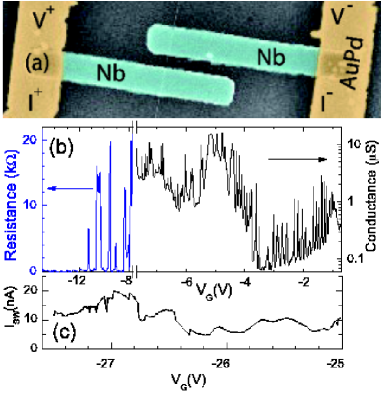
Typical room temperature resistances of our devices are in the range of 5 to 10 k. In Fig. 1 (b) we present electric transport data taken at mK with a fixed bias current of . For gate voltages above about -8 V the conductance is rather low (S) with a transition to nearly equidistant Coulomb peaks above -4 V (S). For V the resistance remains below 20 k and drops to zero in certain regions. For V the sample remains superconducting. At low temperatures the current-voltage (IV) characteristics of the devices show hysteretic switching from a zero or low resistance to a high resistance state as the bias current exceeds a certain value . At mK the switching current varies with the gate voltage and shows, on average, a clear tendency to increase as is tuned more negative. Superimposed on the increasing background we observe a resonant modulation of . At high negative gate voltage we observed sudden changes of the normal state resistance and the switching current indicating the motion of trapped charges in the silicon oxide Fig. 1 (c). In the range V V we found a maximum of nA which is high compared to earlier reports on MWNTs hakonen . This behavior is consistent with an increase of the transparency of the contacts at negative gate voltages, as previously observed in Nb-SWNT-Nb junctions morpurgo . The rather high value of the switching current can be attributed to several factors like the on-chip electromagnetic environment which reduces the switching of the Josephson junction, and the high transparency junctions.
We also checked the stability of our junction against thermal cycling and aging. We cooled down the sample a total of five times over a period of almost six months. It was always possible to identify the two characteristic regions corresponding to Coulomb blockade and supercurrent, approximately in the same gate range. Slight differences in gate voltage range at consecutive cooldowns can be explained by changes of the extrinsic doping level.
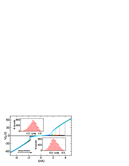
In Fig. 2 we plot the characteristics for different temperatures at V, recorded at the third cooldown where current has been swept from minus to plus. At low temperature the curves show hysteretic switching while, when increasing the temperature, the hysteresis is gradually suppressed. The retrapping current, i.e. the current at which the junction switches back from the normal into the superconducting state, is much less temperature dependent and decreases when the temperature is decreased. Already prior to the switch of the junction from the superconducting to the quasiparticle branch the resistance becomes finite as expected for an overdamped junction with phase diffusion. The hysteretic switching and the phase diffusion can coexist provided that the damping at the plasma frequency is sufficiently strong tinkham ; vion .
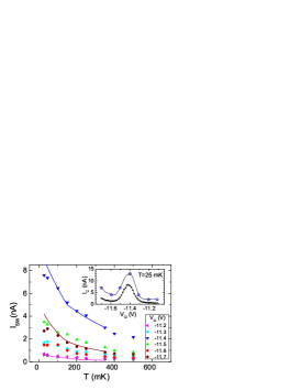
In Fig. 3 we present the temperature dependence of the critical current for different gate voltages at the same resonance. At 300 mK and V we still find a sizable switching current of nA, which greatly facilitates sensor applications. We further studied the statistics of the switching by repeating 5000 sweeps and recording the switching current for each of them. Two examples are plotted in the insets of Fig. 2. We measured a typical full width at half maximum of % at 50 mK.
For the physical interpretation of the data it is important to note that observed temperature dependent switching current can be very different from the intrinsic curve of the junction in absence of thermal fluctuations Fulton74prb . Using a T-independent as single fit parameter, we calculated with the help of an extended RSJ model Kautz90prb containing thermal current noise and the coupling to an external RC circuit which accounts for our on chip electromagnetic environment.
The solid lines in Fig. 3 have been obtained using the measured junction resistance after the switch, the resistance of the external , and pF – the external capacitance. The capacitance of the Josephson junction is estimated as fF, which can be neglected. The importance of fluctuations is quantified by the parameter ( is the Boltzmann-constant). The crossover temperature between the strong () and the weak () regime is determined by the condition , where is the Josephson coupling energy. It is thus clear that in our experiments we operate the crossover region . The agreement between the measured T-dependence of the with the model (solid line in Fig. 3) is good, except at mK where the observed is slightly reduced. In the inset we plot the switching current at 25 mK measured along the resonance and the corresponding critical currents extracted using the the model described.
In the evolution of the current-voltage characteristics three temperature regimes can be distinguished. At low temperatures, the voltage in the SC state is negligible and and we observe hysteretic switching to the high resistance branch and back. At temperature the current voltage curves display a small, but finite voltage below the switching current (phase-diffusion branch), but switching is still present. At high temperatures, , the -curves are smooth without jumps. The critical current is indicated by the maximal curvature of .
When taking into account the effects of fluctuations, no intrinsic -dependence of the critical current remains in the investigated range of temperatures. This indicates that the energy scales controlling the latter exceed 50 V. In fact, both the energy gap of the Nb and the Thouless energy of the nanotube are of the order of 1 mV, i.e., more than an order of magnitude larger. What is the reason for the resonant variation of ? Although multiwall carbon nanotubes are usually disordered, the Coulomb blockade patterns are rather regular in this sample. The Coulomb diamonds close at low bias voltage (not shown), indicating that disorder does not split the tube into several weakly coupled quantum dots as in other cases (in particular for tubes with larger diameter). The spacing of the Coulomb peaks is very even and resembles that of metallic islands with little evidence of a finite level spacing. This may be attributed to the availability of states in the inner shells of the tubes. The supercurrent resonances are accompanied by weaker transmission resonances in the normal state conductance at high magnetic fields (T). It is likely that both are produced by constructive quantum interference of the underlying single particle states, which in presence of weak disorder is more of a conductance fluctuation type rather than regular Fabry-Perot oscillations herrero . At strongly negative gate voltages the overall contact transparency becomes very high, leading to a life-time broadening of the resonances, which exceeds their distance. For this reason the supercurrent remains substantial a between the resonance peaks.
In conclusion we have realized a Josephson junction with a MWNT as weak link and niobium as superconductor. The value of the critical current could be widely tuned by applying a gate voltage. At positive gate voltages the supercurrent was suppressed and the transport was dominated by Coulomb blockade. At negative gate voltage we observed critical currents up to a value of 30 nA. The junction properties are reproducible in successive cooldowns and stable in time. Thanks to the use of niobium, the critical current is robust against temperature and magnetic field, making it suitable for future application in nano-SQUIDs.
We thank L. Forro and C. Miko for providing the carbon nanotubes and T. Novotny and C. Urbina for fruitful discussions. This work was supported by the EU FP6 CARDEQ project and by the Graduiertenkolleg GK638.
References
- (1) B. D. Josephson, Phys. Lett. 1, 251-253 (1962).
- (2) K. K. Likharev, Rev. Mod. Phys. 51, 101-159 (1979).
- (3) M. F. Goffman, R. Cron, A. Levy Yeyati, P. Joyez, M. H. Devoret, D. Esteve, and C. Urbina, Phys. Rev. Lett. 85, 170 (2000).
- (4) J. Clarke, and A. I. Braginski (eds.) The SQUID Handbook (Wiley-VCH, Weinheim, 2004).
- (5) W. Wernsdorfer, Adv. Chem. Phys. 188, 99-190 (2001).
- (6) A. Kasumov, M. Kociak, M. Ferrier, R. Deblock, S. Guéron, B. Reulet, I. Khodos, O. Stéphan, and H. Bouchiat, Phys. Rev. B. 68, 214521 (2003).
- (7) J. P. Cleuziou, W. Wernsdorfer, V. Bouchiat, T. Ondarcuhu, and M. Monthioux , Nature Nanotech. 1, 53 (2006).
- (8) P. Jarillo-Herrero, J. A. van Dam, and L. P. Kouwenhoven, Nature 439, 953 (2006).
- (9) H. I. Jørgensen, K. Grove-Rasmussen, T. Novotný, K. Flensberg, and P. E. Lindelof, Phys. Rev. Lett. 96, 207003 (2006). H. I. Jørgensen, T. Novotný, K. Grove-Rasmussen, K. Flensberg, and P. E. Lindelof, Nano Lett. 7(8), 2441 (2007).
- (10) T. Tsuneta, L. Lechner, and P. Hakonen, Phys. Rev. Lett. 98, 087002 (2007).
- (11) J. M. Martinis, and R. L. Kautz, Phys. Rev. Lett. 51, 14, 1057 (1989).
- (12) A. Morpurgo, J. Kong, C. M. Marcus, H. Dai, Science 286, 263 (1999).
- (13) D. Vion, M. Goetz, P. Joyez, D. Esteve, and M. H. Devoret, Phys. Rev. Lett. 77, 3495, (1996).
- (14) M. Tinkham, Introduction to Superconductivity (McGraw-Hill, Singapore, 1996).
- (15) T. A. Fulton and L. N. Dunkleberger, Phys. Rev. B 9, 4760 (1974);
- (16) R. L. Kautz and J. M. Martinis, Phys. Rev. B 42, 9903 (1990);