Electron transport in a slot-gate Si MOSFET
Abstract
The transversal and longitudinal resistance in the quantum Hall effect regime was measured in a Si MOSFET sample in which a slot-gate allows one to vary the electron density and filling factor in different parts of the sample. In case of unequal gate voltages, the longitudinal resistances on the opposite sides of the sample differ from each other because the originated Hall voltage difference is added to the longitudinal voltage only on one side depending on the gradient of the gate voltages and the direction of the external magnetic field. After subtracting the Hall voltage difference, the increase in longitudinal resistance is observed when electrons on the opposite sides of the slot occupy Landau levels with different spin orientations.
pacs:
73.43.-f; 72.20.-i; 72.25.RbI Introduction
The fabrication of Si-MOSFET samples with a narrow gate barrier or with narrow slots in the gate Haug ; Washburn ; Berkut ; Wang ; vanSon has given rise to new experimental possibilities. In particular, samples with a narrow gate barrier Haug ; Washburn were used for investigation of the backscattering of the edge current in the quantum Hall effect (QHE) regime, while the slot-gate geometry has permitted reliable measurements of a two-dimensional electron transport in case of low electron density Shashkin . In this work, we use the slot-gate geometry to measure the longitudinal resistance in the QHE regime for unequal electron densities along the sample. Our aim was to reveal the influence of the spin-flip process on the electron transport when electrons on the opposite sides of the slot occupy Landau levels (LL) with different spin orientations.
II Experimental results and discussion
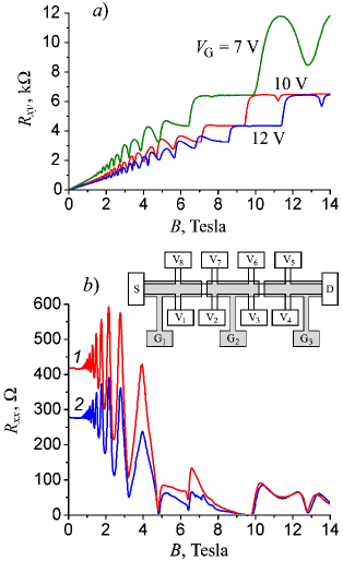
The sample with two narrow slots (100 nm) in the upper metallic gate was similar to that described earlier in Ref. Shashkin (see insert in fig. 1). Application of different gate voltages to the gates , and permitted one to maintain different electron densities in different parts of the sample.
The sample resistance was measured at mK using a standard lock-in technique with the measuring current 20 nA at a frequency of 10.6 Hz. The electron mobility was at m-2.
In the first series of experiments, all gates were connected. The magnetic field dependences of the Hall (transverse) resistance measured between probes – are shown in fig. 1a. The “plateaus” are clearly seen only for Landau filling factors and corresponding to the Hall resistances and , correspondingly. Clear “plateaus” in at are usually not observed in Si-MOSFET being “contaminated” by the “overshoot” effect Richter ; Shlimak1 .
The longitudinal resistance was measured across the gap between voltage probes and and without the gap, between probes and . In zero magnetic field, is 1.5 times larger than (fig. 1b) due to the distance between probes 1 and 2 being 1.5 times larger than that between probes 2 and 3. Therefore, the longitudinal resistance is not affected by the existence of the narrow slot in the gate. In other words, in our sample, the narrow slot in the upper gate does not lead to the existence of a potential barrier. It is remarkable, however, that at magnetic fields above 10 T, both resistance curves merge. This can be explained by the influence of the edge channels edge ; edge1 , so that the length between probes becomes irrelevant.
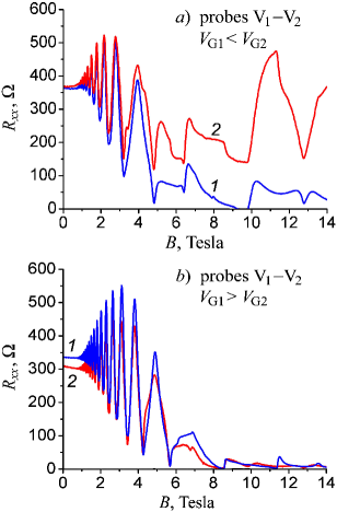
In case of different gate voltages ( was always equal to ), the difference in the transverse Hall voltages appears. is added to the longitudinal voltage only on one side of the sample, depending on the gradient of the gate voltage , which makes the longitudinal resistance non-symmetric: for at given direction of the magnetic field B, was added to the voltage , while for , remains unchanged (fig. 2a,b). On the opposite side of the sample, the situation is reverse: is added to the voltage drop for . It was shown in Ref. Berkut that the sample side where is added to is determined by the vector product . Different values of on the opposite sides of the sample mean that in order to analyse the longitudinal resistance in the case of different gate voltages, one need to subtract properly the contribution of the Hall voltage difference.
In another set of experiments, conducted at mK, the magnetic field was fixed at 8 Tesla, while the gate voltage was varied. First, all gates were connected and was measured between probes and (figure 4, blue line). Using the data shown in fig. 1a, one can conclude that the “plateau” at around V corresponds to the filling factor , while the “plateaus” at around V and V correspond to and , correspondingly.
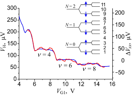
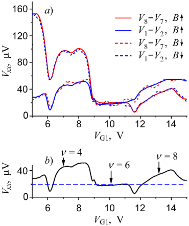
Figure 4a shows measured simultaneously on both sides of the sample between probes – and probes –. was kept constant, while was varied from 5 V to 15 V. In this experiment, the gradient of the gate voltage undergoes a sign change at . If the direction of the magnetic field is reversed, the curves trade places. The difference between the two curves plotted as a function of (fig. 4, red line) practically coincides with . This fact allows us to subtract properly the contribution of the Hall voltage difference: one need to take into account only the lower parts of the both curves. The result is shown in fig. 4b.
Let us discuss the curve shown in fig. 4b. Keeping constant means that electrons underneath the gate always occupy the sixth LL with spin “down” (see fig. 4 and the inset). When is varied from 9 V to 11 V, electrons across the slot occupy the same (6th) LL and, therefore, have the same spin orientation. However, when 7 V9 V and 12 V14 V, the electrons underneath the gate occupy “spin up” LLs 4 and 8, correspondingly. At both filling factors and (indicated in the figure by arrows), the longitudinal resistance increases compared to the case. Possible reason for this resistance increase is some additional scattering Buttiker ; Vakili due to the necessity for electrons to flip their spins when crossing the slot.
Acknowledgements.
I. S. thanks V. T. Dolgopolov and A. A. Shashkin for fruitful discussion and the Erick and Sheila Samson Chair of Semiconductor Technology for financial support. We are grateful to A. Bogush and A. Belostotsky for assistance.References
- (1) R. J. Haug, A. H. MacDonald, P. Streda, and K. von Klitzing, Phys. Rev. Lett. 61, 2797 (1988).
- (2) S. Washburn, A. B. Fowler, H. Schmid, and D. Kern, Phys. Rev. Lett. 61, 2801 (1988).
- (3) A. B. Berkut, Yu. V. Dubrovskii, M. S. Nunuparov, M. I. Reznikov, and V. I. Taly’anskii, JETP Lett. 44, 324 (1986).
- (4) S. L. Wang, P. C. van Son, S. Bakker, and T. M. Klapwijk, J. Phys.: Condens. Matter 3, 4297 (1991).
- (5) P. C. van Son, S. L. Wang, and T. M. Klapwijk, Surface Science 263, 284 (1992).
- (6) A. A. Shashkin, S. V. Kravchenko, V. T. Dolgopolov, and T. M. Klapwijk, Phys. Rev. Lett. 87, 086801 (2001).
- (7) C. A. Richter, R. G. Wheeler, R. N. Sacks, Surface Science 263, 270 (1992).
- (8) I. Shlimak, V. Ginodman, A. B. Gerber, A. Milner, K.-J. Friedland, and D. J. Paul, Europhys. Lett. 69, 997 (2005).
- (9) P. L. McEuen, A. Szafer, C. A. Richter, B. W. Alphenaar, J. K. Jain, A. D. Stone, R. G. Wheeler, and R. N. Sacks, Phys. Rev. Lett. 64, 2062 (1990).
- (10) V. T. Dolgopolov, G. V. Kravchenko, and A. A. Shashkin, Solid State Commun. 78, 999 (1991).
- (11) M. Büttiker, Phys. Rev. B 41, 7906 (1990).
- (12) K. Vakili, V. P. Shkolnikov, E. Tutuc, N. C. Bishop, E. P. De Poortere, and M. Shayegan, Phys. Rev. Lett. 94, 176402 (2005).