Boundary-mediated electron-electron interactions in quantum point contacts
Abstract
An unusual increase of the conductance with temperature is observed in clean quantum point contacts for conductances larger than . At the same time a positive magnetoresistance arises at high temperatures. A model accounting for electron-electron interactions mediated by boundaries (scattering on Friedel oscillations) qualitatively describes the observation. It is supported by numerical simulation at zero magnetic field.
pacs:
73.23.-b, 73.63.RtQuantum point contacts (QPC) are usually formed when two wide 2D
conducting regions are connected by a small constriction. They
exhibit a number of intriguing phenomena among which conductance
quantization Wees88 ; Wharam88 is the most emblematic.
Nowadays QPCs are very common tools for condensed matter
physicists. Examples of recent applications include nuclear spin
manipulation, solid state electron optics or precise electron
counting Applications . Recently, the puzzling low conductance “0.7
anomaly”Thomas96 has attracted most of the attention since
it is related to electron-electron (e-e) interactions. But apart
“0.7 anomaly” it is commonly believed that the physics of QPCs is
well understood using a single-particle picture (See
Ref.Beenakker91, and references therein). On the
contrary, it is well known that the properties of two-dimensional
electron gases (2DEGs) dramatically depend on interactions
Altshuler85 ; Aleiner97 ; Zala01 ; Gornyi ; Renard05 . The related
corrections to the conductance and tunnelling density of states
have their origin in Friedel oscillations (FO) of electron density
around impurities. Friedel oscillations are also known to appear at boundaries
Alekseev98 ; Aleiner98 ; Sablikov and could therefore affect
the properties of nano-scale devices. Interestingly, boundary
mediated FOs were recently shown to be possibly involved in ”0.7
anomaly” physics Rejec06 but this subject is still highly
debated Zozoulenko07 .
In this context we show that e-e
interactions can have a significant influence on transport
properties of clean quantum point contacts even in the large
conductance regime (). We used a combination of
relatively low electron densities, high mobility and low series
resistance to clearly uncover the effects of e-e interactions. It
increases interactions due to reduced screening and ensures that
impurity scattering can be disregarded. Starting from the second
conductance step, the average slope of the conductance versus gate
voltage linearly increases with increasing temperature . At the
same time, the low field magneto-resistance (MR) is non-monotonic
at high and strongly temperature dependent. Some of our
findings are present, although not as evident, in previous works
Hansen02 ; Pyshkin00 ; Cronenwett02 ; Feng99 . They are consistent
with a model of e-e interaction mediated by boundaries which is
supported by numerical simulation at T.
The quantum point contacts were defined employing a split-gates lateral depletion technique Thornton86 on high mobility GaAs quantum wells note . Needle and square shaped samples of various sizes were used to check the influence of the geometry (see Table 1). All samples a have back gate to tune the electron density and some samples have a m-wide center gate to obtain better defined conductance quantization steps when grounded Lee06 . Four-terminal resistance measurements were carried out between mK and K with a standard low-frequency technique at small excitation voltage V to avoid heating effects. Any obvious temperature dependance (activated parallel conduction, anomalous temperature dependance of the series 2DEG or leakage of the gates) was excluded note1 . More than ten samples showed a qualitatively similar behavior.
| Sample | Wafer | Hall bar | point contact | center gate |
|---|---|---|---|---|
| Square1 | 1 | 1 | W=0.6 m; L=0.4 m | yes |
| Square2 | 1 | 1 | W=0.6 m; L=1 m | yes |
| Needle1 | 2 | 2 | W=0.8 m | no |
| Needle2 | 2 | 2 | W=0.6 m | no |
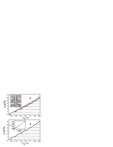
Figure 1a shows the conductance of the sample Square1 as the split-gate voltage is varied for different temperatures. The small () 2DEG series resistance was not subtracted. At low the conductance is quantized to exact integer values of . Note that the “0.7 anomaly” is observed. Increasing temperature not only shrinks the plateaus but also increases the overall slope of resulting in the increase of conductance with . Such a change in the slope of the conductance is not expected from a simple energy averaging, which produces fix temperature independent points in the conductance located at integers of Wees91 . Regions with alternatively positive or negative temperature dependence should be separated by these fixed points. This is not observed in our experiment. It is however possible to restore this behavior by a phenomenological approach. For each temperature a new effective split-gate voltage can be calculated to superpose the curve to the low temperature one (See Fig. 1b). Here, is the pinch off voltage and is the scaling parameter. The strong linear temperature dependence of points at quantum effects, possibly e-e interactions.
In the Hartee-Fock approximation scattering on the potential created by all the other electrons can be considered as the origin of e-e interactions effects Altshuler85 ; Aleiner97 ; Zala01 ; Gornyi ; Aleiner98 ; Sablikov . This potential is connected to the formation of Friedel oscillations of the electron density close to scatterers (defects or boundaries) due to interferences between incoming and reflected electron waves. Spatial variations of their density results in a varying effective potential seen by conducting electrons. In our case the QPC is clean and FOs are created at the boundaries of the constriction. They affect its conductance in two different ways. At low when the thermal length exceeds the QPC width, FOs located in the 2DEG can reduce the conductance at a plateau via scattering of emitted electrons back to the QPC Alekseev98 . As is increased these oscillations are damped and conductance plateaus reach ideal integer value of Yacoby96 . When there remain only FOs located inside the QPC. This corresponds to our experimental conditions ( 1 m at mK). As is further increased the transverse oscillations inside the QPC are damped thus effectively widening the constriction (or equivalently shifting 1D energy levels). One has to compensate by applying a lower to obtain a comparable value of conductance (the curves shift to the left). The scaling can be qualitatively understood as follows. Electrostatically defined QPCs have a parabolic cross section potential , is the effective mass. The width of the channel can be defined as , where is the Fermi level in 2DEG reservoirs. One-dimensional energy levels are written and in a constant capacitance model is proportional to . It follows that . In analogy to the 2D case where the conductivity is renormalized as in the ballistic regime of interaction Zala01 we expect that when (the interaction-induced shift of the closest to Fermi level subband only is considered). Here, is the interaction parameter. This leads to the rescaling with as measured.
This result is consistant with a numerical non-self-consistent
Hartree-Fock simulation. The principle of the computation is first
to calculate the local electron density solving the
one-particle Shrödinger equation in a “soft wall”
electrostatic potential for different chemical potential and
temperature . Indeed, instead of calculating the conductance as
a function of for a varying potential
and fixed , we chose to fix the electrostatic potential and
vary the chemical potential. This greatly simplifies the
calculation because the wave-functions are calculated only once.
It is valid for small interval of split gate voltage (between two
conductance steps). Numerical technique and parameters are
described in Ref. note2, ; Usuki95, .
In analogy to the 2D case, the interaction
correction to the potential is computed as follows , where is the
interaction parameter, is the 2D density of states, and a temperature
high enough to suppress FOs. The obtained correction which
includes only -dependent terms is then used to solve the
transmission problem in the total potential which is now a
function of and note2 . Contrary to 2D systems
containing impurities Zala01 ; Gornyi it is not possible to
relate the interaction parameter to the interaction
constant in a simple way. Close to the boundaries the
electron density drops to zero. This drop is not completely abrupt
and the first Friedel oscillation develops in rarefied
weakly-screening electron gas where e-e interactions become
particularly strong. This is taken into account in our simulation
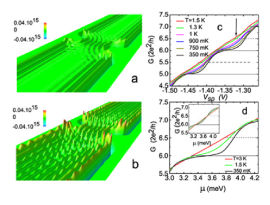
by the large value of the parameter . Figures
2a and b show the obtained correction to the electrons
density in the vicinity of the constriction at
for =3.5 K (a) and =350 mK (b). This
clearly illustrates the formation of FOs as is decreased. Note
that pronounced features are demonstrated despite the use of a “soft wall” model.
Figures 2c and d compare the experimental
conductance of the sample Needle1 to the conductance calculated by
the method described above. In both cases the fix temperature
independent points are missing and the conductance is on average
increasing with temperature. A test of the model consists in
neglecting the interaction term of the scattering potential (i.e.
setting the interaction parameter to 0) which restores the
dependence for energy averaging as expected (Inset to Fig.
2d). An overall good qualitative agreement is obtained
between computer and real experiments which further confirms the
qualitative understanding.
In general, the magnetoresistance reveals important informations about scattering, coherent processes and e-e interactions Gornyi . Figure 3a shows that beside the unusual temperature dependence at T the samples present an unexpected field dependence. The data displayed were measured for sample Needle1 at /h (see arrow in Fig. 2c). At high temperature, the magneto-resistance presents a maximum around mT and becomes negative at higher fields. At low the resistance decreases with at all magnetic fields. The high field slope of the MR is -dependent. Note that the maximum moves to lower fields in QPCs with larger width (not shown).
A linear negative MR with a slope inversely proportional to the width of the channel is known to appear in QPCs VanHouten88 . The increased slope at low temperature that we observe is consistent with the observation at = 0 T which lead to the conclusion that e-e interactions could in principle reduce the effective width of the channel at low . As for the positive MR, it cannot be attributed to diffuse boundary scattering which has very different characteristics Boundary . In particular it is -independent and absent in short constrictions. Similarly, the interplay of boundary scattering and electron collisions Gurzhy95 can be discarded. Finally, commensurability of electron trajectories with the voltage probes can be ruled out since very different Hall bar geometries were tested (Table. 1).
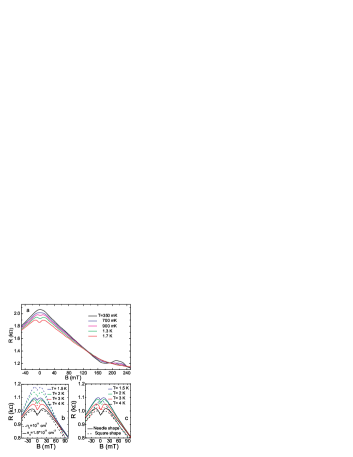
The absence of positive MR at low confirms that the observed quantum effect is due to e-e interaction and is not an interference effect (i.e. Weak anti-localization) which should increase at low . Similarly to 2D systems Zala02 , it can most likely be explained by a variation of the parameter at small magnetic fields which is only visible at high . Note that simulations with -independent did not produce the positive MR. Figure 3b and c demonstrates that the magneto-resistance depends on the electron density and detailed geometry of the point contacts. Carefully adjusting the back- and split-gate voltages, the conductance KT of the sample Needle2 was tuned to the same value () for two different electron densities. Although qualitatively similar, the effect is found to be more pronounced at the lower density. This is consistent with the Friedel oscillation picture which should have in principle smaller effect at high densities when the system resembles a non-interacting Fermi liquid. Figure 3c compares the results of the sample Needle2 to the effect obtained in the sample Square2 at the same density and conductance. The temperature dependence at T is comparable but the field dependence is much more pronounced for the sample Needle2 which has smoother entrances. The geometry dependence therefore appears to be a very interesting tool to study the effect of magnetic field on the measured effect. The positive MR raises interesting questions about the influence of low magnetic field on Friedel oscillations and requires additional theoretical work.
We believe that the presented deviations have not been observed in regular point contacts (for example in Ref. Wees91 ) due to the lower mobility and higher density in these experiments. Indeed, Friedel oscillations are known to depend exponentially on disorder and interaction. However, recent measurements on similar samples show similar phenomenology (see Ref. Pyshkin00, ; Hansen02, ; Cronenwett02, for the conductance quantization and Ref. Feng99, for the MR) indicating that our observation is a general effect. It could have particular importance in nano-scale electronics since boundaries dominate transport properties in nano-devices (electrostatically defined quantum dots, rings, Y-junctions etc.).
Acknowledgements.
We are very grateful to I. Gornyi, A. Dmitriev, K. Takashina, Y. Tokura, K. Pyshkin for helpful discussions and K. Muraki for providing some samples. O.A.T. acknowledges UJF for the invitation as “Maître de Conférences”, the Supercomputing Siberian center and CNRS/IDRIS (project 61778). Part of this work was supported by CNRS/RAS agreement between ISP Novosibirsk and GHMFL Grenoble.References
- (1) B. J. Van Wees et al. Phys. Rev. Lett. 60, 848 (1988).
- (2) D. A. Wharam et al. J. Phys. C. 21, L209 (1988).
- (3) G. Yusa et al. Nature 434, 1001 (2005); B. J. Le Roy et al. Phys. Rev. Lett. 94, 126801 (2005); T. Fujisawa et al Science. 312, 1634 (2006).
- (4) K. J. Thomas et al. Phys. Rev. Lett. 77, 135 (1996).
- (5) C. W. J. Beenakker & H. Van Houten Solid State Physics. 44, 1 (1991).
- (6) B. L. Altshuler & A. G. Aronov Electron-electron interaction in disordered systems. (A. L. Efros, M. Pollak, Amsterdam, 1985).
- (7) A. Rudin, I. Aleiner & L. Glazman Phys. Rev. B 55, 9322 (1997).
- (8) G. Zala, B. N. Narozhny, & I. Aleiner Phys. Rev. B 64, 214204 (2001).
- (9) I. V. Gornyi & A. D.Mirlin Phys. Rev. lett. 90, 076801 (2003); Phys. Rev. B 69, 045313 (2004).
- (10) V. T. Renard et al. Phys. Rev. B 72, 075313 (2005).
- (11) A. Alekseev & V. Cheianov Phys. Rev. B 57, 6834 (1998).
- (12) I. Aleiner & L. Glazman Phys. Rev. B 57, 9608 (1998).
- (13) V. A. Sablikov JETP Lett. 84, 404 (2006); B. S. Shchamkhalova & V. A. Sablikov J. Phys.: Condens. Matter, v. 19, 156221 (2007).
- (14) T. Rejec & Y. Meir Nature 442, 900 (2006).
- (15) S. Ihnatsenka & I. Zozoulenko Phys.Rev. B 76, 045338 (2007).
- (16) A. E. Hansen, A. Kristensen, H. Bruus, Proceedings of NANO-7/ECOSS-21. Malmo, Sweden. 24-28 June 2002.
- (17) K. Pyshkin (Phd Thesis, University of Cambridge, 2000).
- (18) S. Cronenwett et al. Phys. Rev. lett. 88, 226805 (2002).
- (19) Y. Feng et al. J. Vac. Sci. Technol. A 18, 730 (1999).
- (20) T. J. Thornton et al Phys. Rev. lett. 56, 1198 (1986).
- (21) Two wafers were used with the mobility cm2/Vs and cm2/Vs for a density and . They were processed into 10 m wide (type 1) and 100 m wide (type 2) Hall bars.
- (22) H. M. Lee, K. Muraki, E. Y. Chang, & Y. Hirayama, J. App. Phys. 100, 043701 (2006).
- (23) Hall measurements show that the electron density is -independent. The resistance of the 2DEG decreases only by a few Ohms between high and low which makes this source of -dependence incompatible with the observation. Also, the split gate’s leakage current was monitored to be smaller than 20 pA at all voltages and T.
- (24) B. J. Van Wees et al. Phys. Rev. B 43, 12431 (1991).
- (25) A. Yacoby et al. Phys. Rev. Lett. 77, 4612 (1996)
- (26) The computation region was 3 m long and 0.7 m wide. The constriction is 250 nm wide in the model. The calculation step along x and y was 5 nm, the energy step was meV. Usual hopping contant for GaAs were used.
- (27) T. Usuki et al Phys. Rev. B 52, 8244 (1995).
- (28) H. Van Houten et al Phys. Rev. B 37, 8534 (1988).
- (29) T. J. Thornton et al Phys. Rev. lett. 63, 2128 (1989); F. Rahman et al Semicond. Sci. Technol. 14, 478 (1999).
- (30) R. N. Gurzhi, A. N. Kalinenko, & A. I. Kopeliovich Phys. Rev. lett. 74, 3872 (1995).
- (31) G. Zala, B. N. Narozhny, & I. Aleiner Phys. Rev. B 65, 020201 (2001).