Thermal transistor: Heat flux switching and modulating
Abstract
Thermal transistor is an efficient heat control device which can act as a heat switch as well as a heat modulator. In this paper, we study systematically one-dimensional and two-dimensional thermal transistors. In particular, we show how to improve significantly the efficiency of the one-dimensional thermal transistor. The study is also extended to the design of two-dimensional thermal transistor by coupling different anharmonic lattices such as the Frenkel-Kontorova and the Fermi-Pasta-Ulam lattices. Analogy between anharmonic lattices and single-walled carbon nanotube is drawn and possible experimental realization with multi-walled nanotube is suggested.
pacs:
85.90.+h,07.20.Pe, 07.20.-n,63.22.+mI Introduction
Much attention has been devoted in the past years to the study of heat conduction in low-dimensional systems Bonetto . Such study is not only important for understanding the fundamentals of statistical mechanics, but also for potential applications in heat control and management in nanoscale devices.
Indeed, various models for thermal rectifiers/diodes that allow heat to flow easily in one direction have been proposed rec ; diode ; Hu1 ; Hu2 ; nitzan ; J ; J2 ; yang . Moreover, based on the phenomenon of the negative differential thermal resistance (NDTR) observed in nonlinear lattices, a theoretical model for “thermal transistor” is also proposed trt , which allows us to control heat current (due to phonons) by adjusting the temperature of the gate terminal (or called “gate temperature”). This is similar to the electronic transistor which controls the electric current by adjusting the gate voltage. We should point out that our “thermal transistor” is different from the recent “heat transistor”, which controls the heat flux (caused by electrons) via adjusting the gate voltage heattrst . Most recently, based on the thermal transistor, the different thermal logic gats have been also realized theoreticallyWangLi07 , which means that the phonons, the heat carrier, can also be used to carry information and processed accordingly.
The purpose of the current paper are two folds. First, we shall discuss how to improve significantly the switching efficiency of 1D thermal transistor; Second, we shall extend the study from 1D model to 2D which is closer to laboratory fabricated materials.
II One-dimensional model
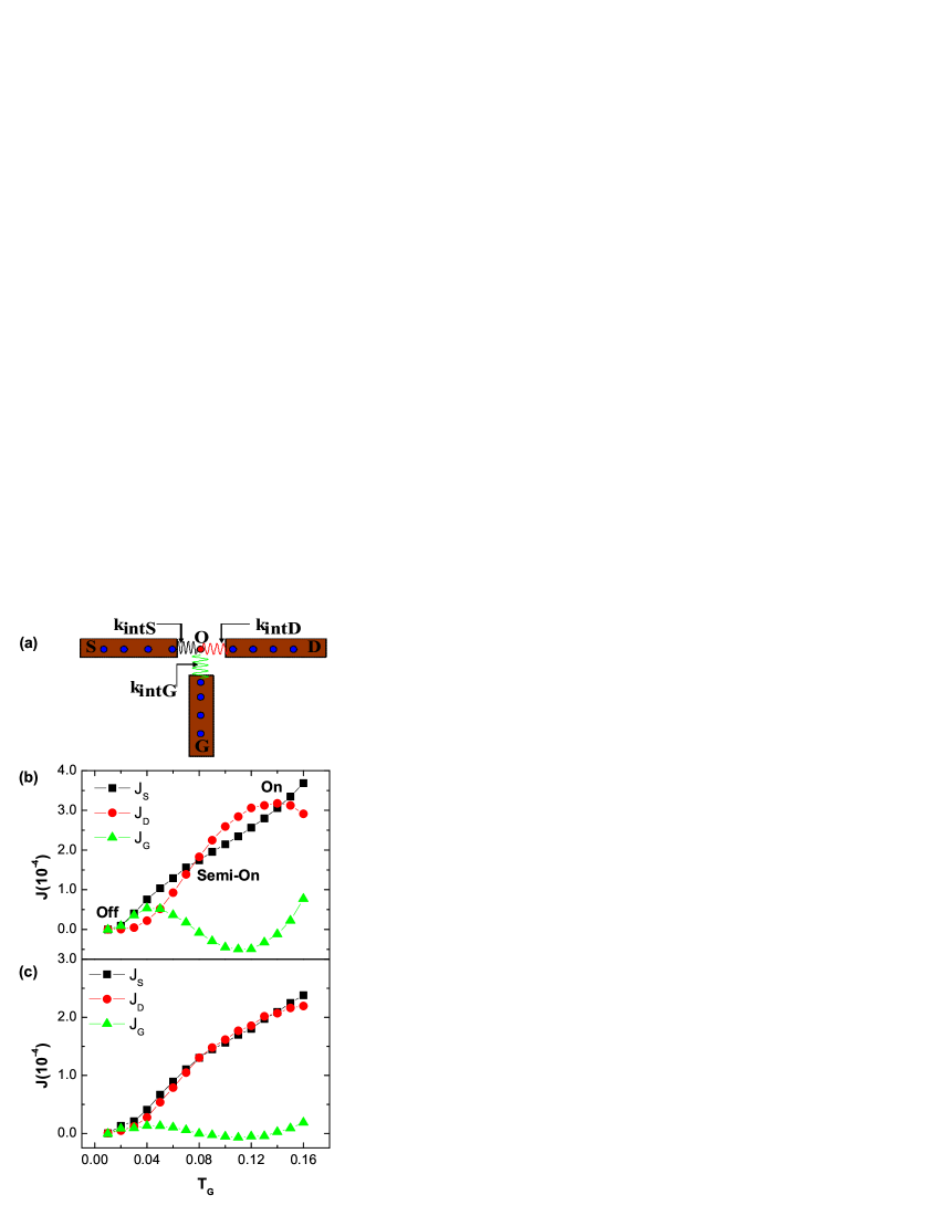
The 1D thermal transistor model consists of three segments S, D, and G and each segment is a Frenkel-Kontorova (FK) lattice braun ; pok . The model configuration, which is shown in Fig. 1(a), is similar to the one proposed in Ref.trt except for an additional interface coupling . In each segment, we regard the particle that is coupled to heat bath as the first particle and the interface particle as the last particle. The total Hamiltonian of the 1D model writes
| (1) |
and the Hamiltonian of each segment can be written as =, with and denote the displacement from equilibrium position and the conjugate momentum of the particle in segment , where stands for S, D or G. The parameters and V are the harmonic spring constant and the on-site potential of the FK lattice. We couple the last particle of segment S, D, and G to particle O via harmonic springs. Thus =. Fixed boundaries are used, i.e., =0 and each segment consists of 10 particles.
In our simulations, we use the Nosé-Hoover heat baths Nose and we set the mass of each particle and the Boltzmann constant to unity unless otherwise stated. In the nonequilibrium stationary state, the heat flux, which is the rate of energy transport, is constant along each segment and the local equilibrium temperature is given by the time average of the square of particle’s velocity per degree of freedom.
We show in Fig. 1 that the model described by Hamiltonian (1) can display different heat controlling features depends on the applied gate temperature, . In particular, the model can act as a heat switch, namely, the system can be switched from a heat insulator to a heat conductor by just adjusting the gate temperature. As demonstrated in Fig. 1(b), when is at 0.01, 0.08, and 0.14, , thus =0, namely, the control terminal does not provide any current to the system, the system, however is switched from an insulating (off) state, to a semi-conducting (semi-on) state, and conducting (on) state. At these three points, are 3.8x, 1.8x, and 3.2x, respectively. The ratio of at the “on” state to that at the “off” state is considered as the switching efficiency which is about 800.
We further demonstrate that the model can act as a heat modulator as well in which can be continuously modulated by the gate temperature. To show this, we recall that for any two weakly coupled lattices, the heat current depends among others, on the strength of the interface coupling used diode ; PRB . Thus, to have , we can reduce the strength of so that the heat flow through the control terminal decreases. Apparently, should not be too small otherwise is not well-controlled by . The numerical result is shown in Fig. 1(c).
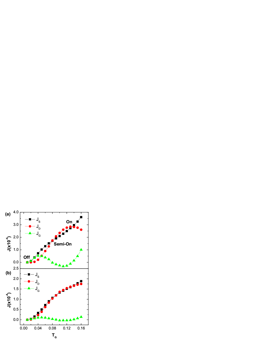
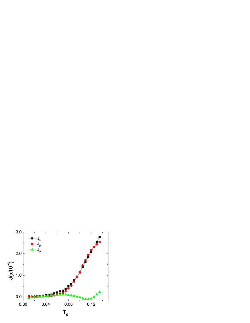
In our next configuration, we replace segment D with a FPU- lattice whose phonon spectrum is contributed by low frequency vibrations (acoustic phonons) only. The Hamiltonian is given by =, with being the anharmonicity. We show in Fig. 2(a) that such a setup reduces the heat current at “off” state greatly but affects the heat current at “on” state only slightly with the switching of about 1300, where equals to 2.15x and 2.82x at =0.01 and 0.14, respectively. It can be noticed that for this and the former lattice choice in the present model, at the “off” and “on” state is about and , respectively, with a switching of about , this is a significant improvement compared with previous one trt . The high switching is mainly a result of the significant reduction of at the “off” state, which is basically due to the lower at “off” state ( in the previous work it is designed at 0.04). Moreover, we found that using lattice with lower heat resistance as terminal D is ideal for achieving a large . In Fig. 2(b), we show the heat modulating effect with the same setup. Since the demonstrated features of the transistor rely very much on an efficient control of the interface temperature, it would be interesting also to study how the property of the control terminal can affect its functions. In Fig. 3, we show that when we use the FPU- lattice as the control segment, due to the large heat resistance in the segment, temperature does not well follow thus heat currents in segment S and D do not sensitively depend on in the low temperature regime. Only when 0.08, significant increment of currents and continuous modulation of are observed. In other words, can be even more precisely adjusted.
The results presented so far have shown that by choosing the lattice in different segment appropriately, one can improve the switching and modulating efficiency significantly. This message is very important and useful for optimization and experimental realization of the thermal transistor. In the following, we shall extend the study of the thermal transistor to 2D. Such extension is important in application, as it takes into account the interaction between longitudinal and transverse motions and therefore is closer to real material such as thin film etc. However, it is not our intention here to look for optimum switching/ modulating condition for this model.
III Two-dimensional model
The displacement from equilibrium position and the momentum of a particle in 2D lattice are labeled as and , respectively. The relative separation between two particles is ==. The Hamiltonian of our model consists of the Hamiltonian of each segment:
| (2) |
and the Hamiltonian of the interface:
| (3) |
Similarly, all segments are coupled to each other via harmonic springs. In our model, segments and are FK lattices and segment is FPU- lattice. Thus, ()=, =+, =0, and =. The harmonic spring constant and the on-site potential may take different values in different segments. Periodic and fixed boundaries are used in the Y (transverse) and X (longitudinal) direction respectively, namely, = and =(0, ) for =. Thus the topologies of the segments, as shown in Fig. 4(a), are cylinders. Nosé-Hoover heat baths are coupled to the ends of segment (=1). In the stationary state, temperature gradients are set up in the direction and thus only heat currents through longitudinal links, (=) need to be taken into account, which are constant along each segment.
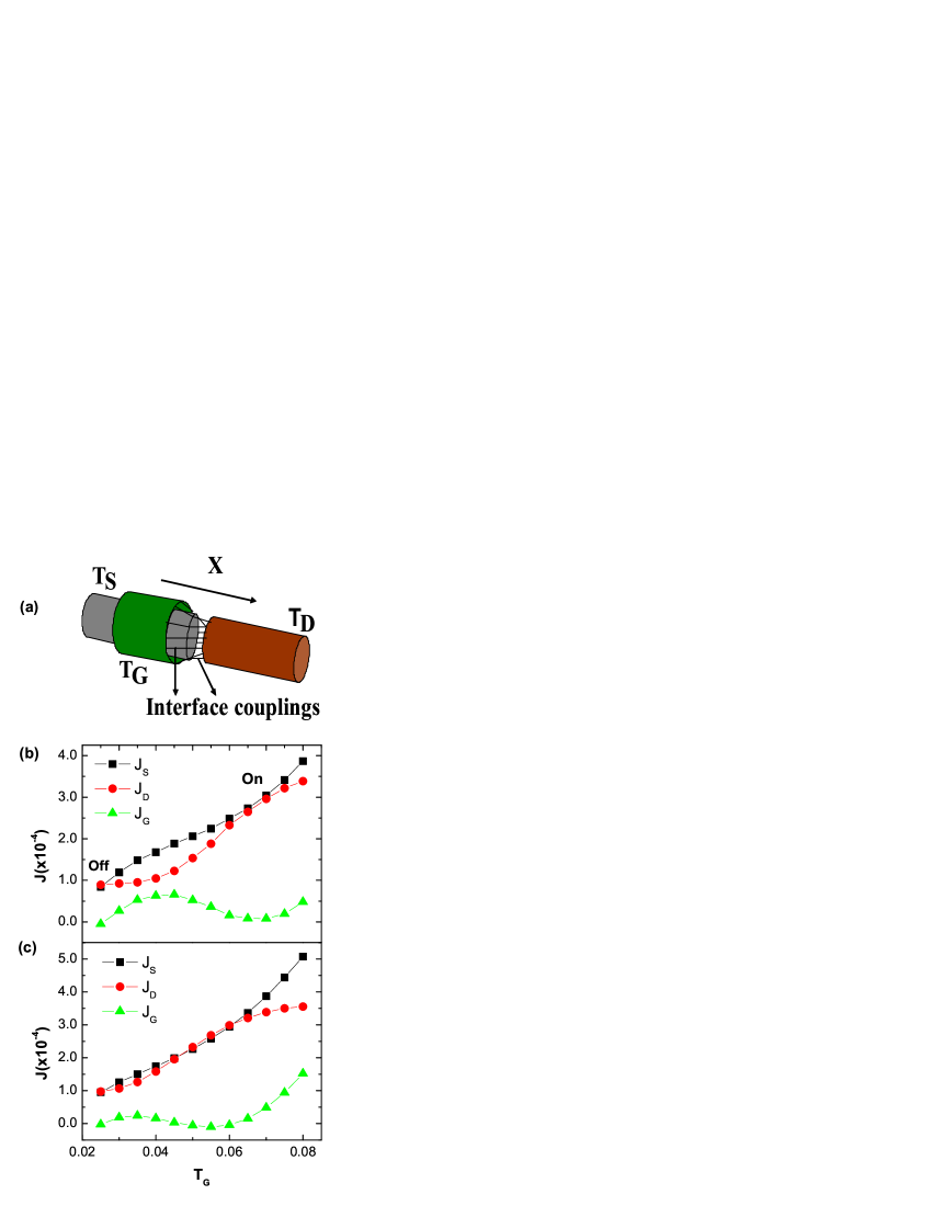
In Fig. 4(b), we show the heat switching for the 2D thermal transistor model. It can be seen that when is at 0.01 and 0.07, and =0. At these two points, are 8.43x and 3.38x respectively and thus the switching efficiency is about 4. This is a significant reduction when compared with the 1D case and this scenario is also quite similar to the 2D thermal rectifier J2 . We show in Fig. 4(c) that when is increased, the difference between and is reduced, which gives a better modulation of by the gate temperature. It is worth mentioning that in 2D case, the crossover energy, particles above which are able to overcome the on-site potential barrier is much lower than that in 1D case. Thus the lattice parameters should be re-designed, otherwise the switching efficiency is reduced significantly as shown above.
IV Discussion and Conclusion
In summary, we have provided several ways in improving the switching efficiency in 1D thermal transistor, namely, one can change different lattice in different segments, and/or by adjusting the coupling strength at the interface. Our study has been extended to two-dimensional lattices and a prototype of 2D thermal transistor - a tube-like model have been proposed. Our numerical simulations have demonstrated that such a prototype can work as a heat switch and a heat modulator - two basic functions of a thermal transistor.
In our numerical simulations, we have used dimensionless units for the sake of computations. However, all dimensionless units are related to the dimensional physical variables through dimensional scaling and consequently, the physical (real) temperature is related to the numerical temperature T through where is the Boltzmann constant (please refer to Bambi1 for details). Suppose we use single-walled carbon nanotube as our experimental prototype for the thermal transistor model, namely with the mass of particle , lattice constant , and natural oscillation frequency correspond to the real values of such a material parameters , =0.01 in our simulations corresponds to physical temperature of about K. Similar analysis for heat flux gives (=) . Therefore, with , is about W (J/s) which is smaller than that one in Ref.Zhang . The smaller heat flux obtained in our model is not surprising. It is mainly due to the interacting with external on-site potential D and the interface thermal resistance arises in coupling dissimilar nonlinear lattices J , which is similar to the case of electronic diode where the electrical current are greatly reduced by the P-N junction. For a homogeneous FPU lattice with similar parameters, can be about 2 orders of magnitude higher.
Even though a real working prototype for solid state thermal transistor is still an open issue, we believe that the above model or its variants will be realized sooner or later. Moreover, a solid state thermal rectifier using nanotubes has been experimentally demonstrated chang1 (see also Refwuli for other variants). More recently, a tunable and reversible thermal link using multi-walled carbon nanotubes (MWCNTs) chang2 were successfully demonstrated whereby the thermal conductance can be controlled mechanically by displacing the outer shell with respect to the inner one. This is a step forward to the realization of thermal transistor. In fact, in the heat control models, be it a thermal rectifier or a thermal transistor, the key factors are: (1) the broken of the spatial symmetry of terminal, namely they are two different materials; (2) nonlinearity in each segment. Therefore, the possible material to be used for the thermal transistor might be multiwalled nanotubes. As the recent experiment chang2 shows that the outer wall can be used to control the thermal conductance of the nanotube, thus it can be used as the controlling terminal G.
Acknowledgment
The work is supported partially by an academic research fund, R-144-000-203-112 from MOE of Singapore, and the Temasek Young Investigator Award of DSTA Singapore under Project Agreement POD0410553
References
- (1) F. Bonetto, J. L. Lebowitz, and L. Rey-Bellet: Mathematical Physics 2000, edited by A. Fokas, A. Grigoryan, T. Kibble, and B. Zegarlinsky, (Imperial College Press, London, 2000), (pp. 128-150); B. Li, J. Wang, L. Wang, and G. Zhang: Chaos 15 (2005) 015121.
- (2) M. Terraneo, M. Peyrard, and G. Casati: Phys. Rev. Lett. 88 (2002) 094302.
- (3) B. Li, L. Wang, and G. Casati: Phys. Rev. Lett. 93 (2004) 184301.
- (4) B. Li, J. Lan, and L. Wang: Phys. Rev. Lett. 95 (2005) 104302.
- (5) J. Lan and B. Li: Phys. Rev. B 74 (2006) 214305.
- (6) D. Segal and A. Nitzan: Phys. Rev. Lett. 94 (2005) 034301.
- (7) B. Hu, L. Yang, and Y. Zhang: Phys. Rev. Lett. 97 (2006) 124302.
- (8) B. Hu and L. Yang: Chaos 15, 015119 (2005).
- (9) N. Yang, N. Li, L. Wang, and B. Li: Phys. Rev. B 76 (2007) 020301 (R).
- (10) B. Li, L. Wang, and G. Casati: Appl. Phys. Lett. 88 (2006) 143501 .
- (11) O.-P. Saira, M. Meschke, F. Giazotto, A. M. Savin, M. Möttönen, J. P. Pekola: Phys. Rev. Lett. 99 (2007) 027203.
- (12) L. Wang and B. Li: Phys. Rev. Lett. 99 (2007) 177208.
- (13) O. M. Braun and Y. S. Kivshar: Phys. Rep. 306 (1998) 1.
- (14) V. L. Pokrovsky and A. L. Talapov: Theory of Incommensurate Crystals, Soviet Scientific Reviews Supplement Series, Physics Vol. 1 (Harwood, New York, 1984).
- (15) S. Nosé: J. Chem. Phys. 81 (1984) 511; W. G. Hoover, Phys. Rev. A 31 (1985) 1695.
- (16) K. R. Patton and M. R. Geller: Phys. Rev. B 64 (2001) 155320.
- (17) B. Hu, B. Li, and H. Zhao: Phys. Rev. E 57 (1998) 2992 .
- (18) K. Aoki and D. Kusnezov: Phys. Rev. Lett. 86 (2001) 4029; H. Kaburaki and M. Machida, Phys. Letts. A 181 (1993) 85.
- (19) For carbon atom, with the mass =1.98xkg, lattice constant m, and the natural oscillation frequency 4.53xs-1 (if we take for example E=30meV carbon ), 2.95x and 1.84x.
- (20) G. Zhang and B. Li: J. Chem. Phys. 123 (2005) 114714. For a (9,0) single-walled carbon nanotube whose ends are thermalized with Nosé-Hoover heat baths at =310K and 290K, is about 5.26x W. With roughly 4 carbon atoms per cross section of the nanotube, can be further approximated to about W.
- (21) D. Donadio and G. Galli: Phys. Rev. Lett. 99 (2007) 255502.
- (22) C. W. Chang, D. Okawa, A. Majumdar, and A. Zettl: Science 314 (2006) 1121.
- (23) G. Wu and B. Li: Phys. Rev. B 76 (2007) 085424.
- (24) C. W. Chang, D. Okawa, H. Garcia, T. D. Yuzvinsky, A. Majumdar, and A. Zettl: Appl. Phys. Lett. 90 (2007) 193114.
- (25) S. Rols, Z. Benes, E. Anglaret, J. L. Sauvajol, P. Papanek, J. E. Fischer, G. Coddens, H. Schober, and A. J. Dianoux: Phys. Rev. Lett. 85 (2000) 5222.